
Recommended
More Related Content
Similar to Optoelectronics is a branch of physics and technology
Similar to Optoelectronics is a branch of physics and technology (20)
Recently uploaded
Recently uploaded (20)
Optoelectronics is a branch of physics and technology
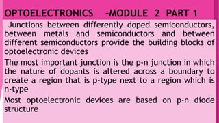
- 1. OPTOELECTRONICS -MODULE 2 PART 1 Junctions between differently doped semiconductors, between metals and semiconductors and between different semiconductors provide the building blocks of optoelectronic devices The most important junction is the p-n junction in which the nature of dopants is altered across a boundary to create a region that is p-type next to a region which is n-type Most optoelectronic devices are based on p-n diode structure
- 2. It is a junction between a p-type and n-type Semi- conductor If a p-n junction consists of p-type and n-type section of the same semi-conductor material it is called a homojunction If the junction consists of two different type of semi- conductor material it is called a heterojunction p-n junction can be formed in different ways. The simplest formation is bringing p and n type SC together using the crystal growth technique The p-n junction is fabricated either by growing p-type material on a n-type material / vice-versa
- 3. The general technique used in crystal growth are epitaxial growth, diffusion and ion-implantation 1. Epitaxial growth where the dopant species are simply switched at a particular instant of time 2. Diffusion here dopants are selectively diffuses into oppositely doped semiconductor 3. Ion-implantation in which the dopant ions are implanted at high energies into the semiconductor
- 4. A p-n junction consists of p-type and n-type section of semi-conductor materials in metallurgical contact. The p-type has an abundance of holes (majority carriers) and few mobile electrons (minority carriers), and n-type region has an abundance of mobile e-s (majority carriers) and few holes (minority carriers) Both charge carriers are in continuous and random thermal motion in all directions
- 5. When two regions are brought into contact, the following consequences of events take place: 1. Electrons and holes diffuse from areas of high concentrations towards the areas of low concentrations. Thus e-s diffuse from n- region into p-region leaving behind +vely charged ionized donor atoms
- 6. In the p- region the e-s combine with the abundant e+s Similarly the e+s diffuse from p-region into n-region leaving behind –vely charged ionized acceptor atoms. In the n-region these e+s recombines with abundant mobile e-s This diffusion process does not continue indefinitely, however because it causes a disruption of the charge carriers balance 2. As a result a narrow region on both sides of the junction becomes nearly depleted of mobile charge carriers leads to a depletion region(layer) The thickness of this layer is inversely proportional to the concentration of dopants in the region
- 7. 3. The fixed charges create an electric field in the depletion layer that points from the n-side towards the p-side of the junction. The built-in field obstructs the diffusion of further mobile carriers through the junction region 4. An equilibrium condition is established that results in a net built-in potential difference Vo between the two sides of the depletion region with n-side exhibiting high potential than p-side 5. The built–in potential provides a lower potential energy for an e- on n-side relative to p-side. As a result the energy bands bend as in fig. below
- 9. 6. No current flows across the junction. The currents associated with diffusion and built-in field cancel for both the e-s and e+s The Biased p-n junction An externally applied potential will alter the potential difference between p and n regions This in-turn will modify the flow of majority carriers, so that the junction can be used as a gate. If the junction is forward biased by applying a positive voltage to the p-region , its potential is increased with respect to n-region so that the electric field is produced in a direction opposite to that of built-in field The presence of the external bias voltage causes a departure from equilibrium and a mis-alignment of Fermi-levels in the p and n-regions , as well as in the depletion layer
- 10. The presence of two Fermi-levels in the depletion layer Efc and Efv represents the state of quasi equilibrium
- 11. The net effect of the forward bias is to reduce the height of the potential-energy hill by an amount eV The majority carrier current turns out to increase by an exponential factor exp (eV/kT) so that the net current becomes ί = ίs exp (eV/kT) – ίs where ίs is constant The excess majority carriers , holes and electrons that enter the n and p regions, become minority carriers and recombine with the local majority carriers this process is minority carrier- injection
- 12. If the junction is reverse biased by applying a negative voltage V to the p-region, the height of the potential- energy hill is augmented by eV. This impedes the flow of majority carriers. The corresponding current is multiplied by the exponential factor(eV/kT), when V is negative The net result for the current is ί = ίs exp (-eV/kT) – ίs ⋍ ίs So that a small current of magnitude ⋍ ίs flows in the reverse direction Hence the ideal I-V characteristics is given by ί = ίs exp (eV/kT) – 1 Shockely equation
- 13. In the ideal diode model, an abrupt junction is assumed between the uniformly doped n- and p- regions In addition certain assumptions are also made: 1. The current flow across the diode is one-dimensional 2. All the applied voltage appears across the space charge region and the neutral regions are field free. Thus the minority carrier currents in the neutral n- and p-regions can be described as diffusion currents only 3. There is no net generation or recombination of carriers in the junction depletion region which means that the electron and hole currents remain constant throughout this region
- 14. 4. Low-level injection prevails on both sides of the junction. This condition places a restriction on the current that can be drawn through the ideal diode and is not valid at high currents 5. The Boltzmann relation for electrons and holes is valid throughout the depletion region. The Boltzmann relation is a direct consequence of the balance between the drift and diffusion processes in the depletion region. Since the current drawn through the junction is quite small compared to the equilibrium diffusion or drift current, this balance is approximately maintained
- 16. The response of a p-n junction to a dynamic applied voltage is determined by solving the set of differential equations governing the processes of electron and hole diffusion, drift ( under the influence of the built-in and external fields) and recombination. Heterojunctions: Junctions between different semi-conductor materials are known as heterojunctions Optical sources and detectors make extensive use of heterojunctions and their designs , they are used not only as active regions , but also as contact layers and waveguiding regions The importance of hetero junctions are the following:
- 17. 1. Junction between materials of different band-gap create localized jumps in the energy band diagram. A potential- energy discontinuity provides a barrier that can be useful in preventing selected charge carriers from entering the regions, where they are undesired This property may be used in p-n junctions (ie, to reduce the proportion of the current carried by minority carriers and thus to increase the injection efficiency)
- 18. 2. Discontinuities in the energy –band diagram created by two heterojunctions can be useful for confining charge carriers to a desired region of space. For example , a layer of narrow band-gap material can be sandwiched between two layers of a wider band-gap material, as shown in the p-p-n structure above which consists of a p-p heterojunction and a p-n heterojunction. This double heterostructure(DH) configuration is used effectively in the fabrication of LEDs 3. Heterojunctions are useful for creating energy-band discontinuities that accelerate carriers at specific locations. The additional kinetic energy suddenly imparted to a carrier can be useful for selectively enhancing the probability of impact ionization in a multilayer heterojunctions as in Avalanche photodiode
- 19. 4. semi-conductors of different band-gap type(direct and indirect) can be used in the same device to select regions of structure where light is emitted. Practically only direct band-gap semiconductor type effectively emit light 5. semi-conductors of different bandgap can be used in the same device to select regions of the structure where light is absorbed. Semi-conductor materials whose bandgap energy is larger than the photon energy incident on them will be transparent , acting as a window layer 6. Heterojunctions of materials with different refractive indexes can be used to create photonic structures and optical waveguides that confine and direct photons in certain optical devices
- 20. Junction Theory p-n junction: The PN junction diode consists of a p-region and n-region separated by a depletion region where charge is stored. However, if we were to make electrical connections at the ends of both the N-type and the P-type materials and then connect them to a battery source, an additional energy source now exists to overcome the potential barrier. The effect of adding this additional energy source results in the free electrons being able to cross the depletion region from one side to the other. The behaviour of the PN junction with regards to the potential barrier’s width produces an asymmetrical conducting two terminal device, better known as the PN Junction Diode.
- 21. The depletion layer widens with an increase in the application of a reverse voltage and narrows with an increase in the application of a forward voltage. This is due to the differences in the electrical properties on the two sides of the PN junction resulting in physical changes taking place. One of the results produces rectification as seen in the PN junction diodes static I-V (current-voltage) characteristics. Rectification is shown by an asymmetrical current flow when the polarity of bias voltage is altered as shown below.
- 23. There are two operating regions and three possible “biasing” conditions for the standard Junction Diode and these are: • 1. Zero Bias – No external voltage potential is applied to the PN junction diode. • 2. Reverse Bias – The voltage potential is connected negative, (-ve) to the P-type material and positive, (+ve) to the N-type material across the diode which has the effect of Increasing the PN junction diode’s width. • 3. Forward Bias – The voltage potential is connected positive, (+ve) to the P-type material and negative, (- ve) to the N-type material across the diode which has the effect of Decreasing the PN junction diodes width.
- 24. 1. The p-n junction in Equilibrium (Zero Biased Junction Diode) A p-n junction may be fabricated as a single crystal of semiconductor by a no. of different techniques. Indeed the exact behavior of a junction depends to a large extent on the fabrication process used, which in turn determines the distances over which the change from p- to n- type nature occurs For mathematical convenience we shall assume that the junction is abrupt , that is there is a step change in impurity type as shown in fig. below, which also shows the corresponding carrier concentrations also
- 26. Let Pp and np be the carrier concentrations of holes and electrons on p-side and nn and np that of n-side of the junction respectively. These apply only at relatively large distances from the junction ; close to the junction they are modified Let us assume that the junction is formed by bringing initially isolated pieces of n-type and p-type materials into intimate contact Then since there are many more holes in p-type than in n- type material , holes will diffuse from the p- to n- region The holes diffusing out of p-type side leave behind ionized acceptors, thereby building up a negative space charge layer in p-type side close to the junction
- 27. Similarly electrons diffusing into the p-side, leave behind a positive space charge layer of ionized donors as in fig.(c) below This double space charge layer causes an electric field to be set up across a narrow region on either side of the junction, directed from the n- to p-type region as in fig. below The direction of the junction electric field is such as to inhibit further diffusion of the majority carriers , though such diffusion is not prevented altogether This must so, since the electric field will sweep minority carriers across the junction so that there is a drift current of electrons from p- to the n- type side and holes from n- to p- type side, which is in opposite direction to the diffusion current
- 29. The junction field thus builds up until these two current flows are equal, at which stage the Fermi-level is constant across the junction as shown in fig.(b) above, indicating that equilibrium has been reached within the crystal as a whole. Thus as there is no net current flow in equilibrium Jh (drift) + Jh (diff) = 0 and Je (drift) + Je (diff) = 0 The induced electric field establishes a contact or diffusion potential Vo between the two regions and the energy bands of p-type side are displaced relative to those of n-type side as shown in fig.(b)
- 30. The magnitude of the contact potential depends on the temperature and the doping levels The contact potential is established across the space charge region, which is also referred to as the transition or depletion region so-called because this region has been almost depleted of its majority carriers. As a consequence it is very resistive relative to the other (so-called bulk) regions of the space) An expression relating the contact potential to the doping levels can be obtained , adopting the notations used in the figs above, we can write the electron concentration in the conduction band of p-type as np = Nc exp [-(Ecp-Efp/kT)] where Nc is the effective density of states in the conduction band of p-type
- 31. Similarly, the electron concentration in the n-type side is, nn = Nc exp [-(Ecn-Efn/kT)] where Nc is the effective density of states in the conduction band of n-type Now as mentioned , the Fermi-level is a constant everywhere in equilibrium so that Efp = Efn =EF Hence eliminating Nc we get, Ecp – Ecn = kT ln (nn/np) =eVo Therefore Vo = (kT/e) ln (nn/np) At temperatures in the range 100K ≾ T ≾ 400K, the majority carrier concentrations are equal to the doping levels, that is nn = Nd and Pp = Na and remembering np = ni 2
- 32. We can write the above equation as Vo = kT/e ln (Na Nd/ ni 2) From the above equations we get a very useful relationship between the carrier concentrations on the two sides of the junction, that is given by np = nn exp (-eVo /kT) and similarly Pn = Pp exp (-eVo /kT)
- 33. An “Equilibrium” or balance will be established when the majority carriers are equal and both moving in opposite directions, so that the net result is zero current flowing in the circuit. When this occurs the junction is said to be in a state of “Dynamic Equilibrium“. The minority carriers are constantly generated due to thermal energy so this state of equilibrium can be broken by raising the temperature of the PN junction causing an increase in the generation of minority carriers, thereby resulting in an increase in leakage current but an electric current cannot flow since no circuit has been connected to the PN junction.
- 34. 2. Current flow in Forward Biased PN Junction Diode: if the equilibrium situation is disturbed by connecting a voltage source externally across the junction there will be a net current flow. The junction is said to be forward biased, if the p-region is connected to the positive terminal of the voltage source as shown in fig.(a) As we mentioned in the last section, the depletion region is very resistive in comparison to the bulk regions so that the external voltage V is dropped almost entirely across the depletion region This has the effect of lowering the height of the potential barrier to (Vo-V) as in fig.(b)
- 36. Consequently, majority carriers are able to surmount the potential barrier much more easily than in equilibrium case so that the diffusion current becomes much larger than the drift current. There is now a net current from p- to the n- region in the conventional forward sense and carriers flow in from the external circuit to restore equilibrium in the bulk regions We note that with the application of an external potential the Fermi-levels are no longer aligned across the junction The reduction of the height of the potential barrier leads to majority carriers being injected across the junction
- 37. On being so injected, these carriers immediately become minority carriers, and the minority carrier concentrations near to the junction rise to new values np` and Pn` This establishes excess minority carrier concentration gradients as shown in fig., so that the injected carriers diffuse away from the junction. This is the situation of minority carrier injection and diffusion So considering the n- region, the injected holes diffuse away from the junction recombing as they do so. The electrons lost in this recombination are replaced by the external voltage source so that current flows in the external circuit
- 39. A similar argument applies to the p-region , with roles of electrons and holes reversed, it should be noted that the majority carrier concentrations are not noticeably changed as a consequence of the injection, unless the bias voltage is almost equal to Vo, resulting in a very large current flow The drift current is relatively insensitive to the height of the potential barrier since all the minority carriers generated within about a diffusion length of the edge of the depletion region may diffuse to the depletion region and be swift across it, whatever the size of the electric field there With these arguments we can write the relationship between the minority carrier concentrations in the bulk regions adjacent to the depletion layer as
- 40. np` = nn exp[-e(Vo-V)/kT] and pn` = pp exp[-e(Vo-V)/kT] but for steady state equilibrium we have Pn = Pp exp (-eVo /kT) So, pn` = Pn exp(eV/kT) This shows the excess minority carrier concentration will decrease owing to the recombination in accordance with steady-state equilibrium so that we may write the excess hole concentration in the n- region at a distance x from the edge of depletion layer as ∆p(x)= ∆p(0)exp(-x/Lh), where Lhis the hole diffusion length So, in this case we can write ∆p(x) = pn`(x) – pn and ∆p(0) is the value of ∆p(x) at x=0, that is (pn`- pn )
- 41. We can therefore write ∆p(0) = pn [exp(eV/kT) -1] We have assumed a one dimensional carrier flow in the X-direction , which is an acceptable approximation even though in practice carrier flow occurs in three dimensions Now we have argued that the electric field in the bulk regions are very small and therefore , adjacent to the depletion layer in the n-region , and particularly at x=0, the total current density will be due to diffusion only Thus the current density due to hole motion in this case becomes Jh = (eDh/Lh )∆p(0) exp(- x/Lh)
- 42. Here Dh is the hole diffusion coefficient At x=0, we can write this, (substituting for ∆p(0) Jh = (eDh/Lh) Pn[exp(eV/kT) -1] There is a similar contribution due to electron flow, so current density due to electron motion is given by Je = (eDe/Le) np[exp(eV/kT) -1] Hence the total current density J = Jo [exp(eV/kT) -1] where Jo = e[(Dh/Lh)Pn + (De/Le)np] Jo is called the saturation current density
- 43. In forward biased case, the negative voltage pushes or repels electrons towards the junction giving them the energy to cross over and combine with the holes being pushed in the opposite direction towards the junction by the positive voltage. This results in a characteristics curve of zero current flowing up to this voltage point, called the “knee” on the static curves and then a high current flow through the diode with little increase in the external voltage as shown below.
- 44. The application of a forward biasing voltage on the junction diode results in the depletion layer becoming very thin and narrow which represents a low impedance path through the junction thereby allowing high currents to flow. The point at which this sudden increase in current takes place is represented on the static I-V characteristics curve above as the “knee” point.
- 45. 3. Current flow in a reverse biased p-n junction: In this case the external bias is applied so that the p- region is connected to the negative terminal of the voltage source as in fig.(a). This has the effect of increasing the height of the potential barrier to Vo+V (fig.(b), thereby reducing the diffusion current to negligible proportions
- 46. The net current flow is therefore the drift current which is directed in the conventional reverse sense , that is from the n- to p- region This results in carrier extraction rather than injection because the minority carriers generated near the junction diffuse to it and are swept across the depletion region. The nearer the carriers are generated to the junction, the greater is the probability of this occurring so that a concentration gradient is formed towards the junction as shown in fig. The drift of the carriers across the junction is therefore fed by the diffusion so that we may use precisely the same argument to derive the current-voltage relationship as we used in the previous case.
- 47. The same equation also apply in this case , only difference being , of course that sign of V is changed
- 48. The net result is that the depletion layer grows wider due to a lack of electrons and holes and presents a high impedance path, almost an insulator and a high potential barrier is created across the junction thus preventing current from flowing through the semiconductor material. This condition represents a high resistance value to the PN junction and practically zero current flows through the junction diode with an increase in bias voltage. However, a very small reverse leakage current does flow through the junction which can normally be measured in micro-amperes ( μA ).
- 49. One final point, if the reverse bias voltage VR applied to the diode is increased to a sufficiently high enough value, it will cause the diode’s PN junction to overheat and fail due to the avalanche effect around the junction. This may cause the diode to become shorted and will result in the flow of maximum circuit current, and this shown as a step downward slope in the reverse static characteristics curve below.
- 50. Deviations from the simple theory The theory discussed now is reasonable agreement with what is observed in practice, there are several points of difference For our purposes one of the most important deviations is that , at sufficiently large values of reverse bias , breakdown occurs. That is there is a sudden and rapid increase in reverse current at a particular value of reverse bias voltage as in fig.(b) Reverse breakdown occurs by two mechanisms. The first is called Zener effect is due to quantum mechanical tunnelling
- 52. This takes place most readily in heavily doped junctions, which leads to narrow depletion layers and therefore high junction fields In effect we can see from fig.(a), the energy bands on two sides of the junction become crossed so that the filled states in the valence band of p-side are aligned with empty states in the conduction band of n-side. Electrons therefore tunnel from the p- to n- side vastly increasing the reverse current. The second mechanism is Avalanche breakdown occurs in lightly doped junctions with wide depletion layers This mechanism involves impact ionization of the host atoms by the energetic carriers
- 53. If the carriers crossing the depletion layer acquire sufficient energy from the electric field between the collisions, they may ionize lattice atoms on colliding with them. The electrons and holes so produced may, in turn, cause further ionizing collisions and so on to generate an avalanche of carriers Neither breakdown mechanism is in itself destructive to the junction. If, however, the reverse current is allowed to become too large then Joule heating may cause damage to the device Other important deviations arise from such factors as carrier generation and recombination within the depletion layer
- 54. Carrier generation in the depletion layer gives rise to a larger value of reverse bias current than the simple theory predicts. Optical generation of carriers within the depletion layer may rise to an increase in reverse current or initiate avalanche breakdown if the reverse bias is sufficiently great. These phenomena form the basis of the working of Photodiodes
- 55. Carrier Distribution in p-n Homojunctions: The carrier distribution in p-n junctions depends on the diffusion constant of the carriers. The diffusion constant of the carriers is not easily measured ,more common is the measurement of the carrier mobility and the diffusion constant can be inferred from carrier mobility by Einstein relation which for non-degenerate semiconductors , is given by Dn = (kT/e)μn & Dp = (kT/e)μn Carriers injected into a neutral semiconductor , with no external electric field applied , propagate by diffusion. If the carriers are injected into a region with opposite conductivity type, the minority carriers will eventually recombine
- 56. The mean distance a minority carrier diffuses before recombination is the diffusion length Electrons injected into a p-type region will, on average diffuse over the diffusion length Ln, before recombining with holes. This diffusion length is given by Ln = √Dnτn & Lp = √Dpτp Where τn and τp are electron and hole minority carrier life-times respectively In typical semiconductors , the diffusion lengths is of the order of several micrometers
- 57. The distribution of carriers in a p-n junction under zero and under forward bias is as shown in fig.(a) and (b) below
- 58. Note that minority carriers are distributed over quite a large distance Furthermore the minority carrier concentration decreases as these carriers diffuse further into adjacent region . Thus recombination occurs over a large region , with a strongly changing minority carrier concentration As shown, the large recombination region in homojunctions is not beneficial for efficient recombination While in heterojunctions, carriers are confined by the heterojunction barriers (fig.(c))
- 59. Carrier Distribution in p-n Heterojunctions: All high-intensity light –emitting diodes do not use homojunction design but rather employ heterojunctions, which have clear advantages over homojunction devices Heterojunction devices employ two types of semiconductors , namely a small bandgap active region and a large bandgap barrier region. If a structure consists of two barriers , ie, two large bandgap semiconductors , then the structure is called a double heterostructure, abbreviated as DH The effect of heterojunctions on the carrier distribution is shown in fig.(c) above
- 60. Carriers injected into the active region of the double heterostructure are confined to the active region by means of the barriers As a result the thickness of the region in which carriers recombine is given by the thickness of the active region rather the diffusion length The consequences of this change are significant. We assume that the thickness of the active region is much smaller than the typical diffusion length Diffusion lengths may range from 1μm to 20 μm. Thus the carriers in the active region of a double heterostructure have a much higher concentration than carriers in homojunctions, which are distributed over several diffusion lengths
- 61. It is also noted that a high concentration of carriers in the active region increases the radiative recombination rate and decreases the recombination life-time For this reason, all high-efficiency LED designs employ double heterostructure or quantum well designs. The Effect of Heterojunctions on Device resistance: The employment of heterostructures allows one to improve the efficiency of LEDs by confining carriers to the active region , thereby avoiding diffusion of minority carriers over long distances Heterostructures can also be used to confine the light to waveguide regions ; in particular in Edge emitting LEDs
- 62. Generally modern semiconductor LEDs and Lasers have many heterojunctions for contact layers, active regions and waveguiding regions Even though heterojunctions are useful for improved LED designs, there are certain problems associated with them as: The resistance caused by the heterointerface The origin of the resistance is illustrated in fig. (a), which shows the band diagram of a hetero structure The heterostructure consists of two semiconductors with different band gap energy and it is assumed that both sides of a heterostructure are of n-type conductivity
- 64. Carriers in the large band gap material will diffuse over to small band gap material where they occupy conduction band states of lower energy As a result of electron transfer, an electrostatic dipole forms , consisting of a positively charged depletion layer with ionized donors in the large band gap material, and a negatively charged electron accumulation layer in the small band gap material The charge transfer leads to the band bending illustrated as in fig.(a) above Carriers transferring from one semiconductor to the other must overcome this barrier by either tunneling or by thermal emission over the barrier
- 65. The resistance caused by heterojunctions can have a strong deleterious effect on device performance, especially in high power devices The thermal power produced by heterostructure resistances leads to heating of the active region, thereby decreasing the radiative efficiency It has been shown that these type of heterostructure band discontinuities can be completely eliminated by grading of the chemical composition of the semiconductor in the vicinity of the heterostructure The band diagram of a graded heterostructure is shown in fig.(b) above
- 66. Inspection of the above figure reveals that there is no longer a spike in the conduction band which hinders the electron flow It has been shown that the resistance of parabolically graded heterostructures is comparable to bulk material resistance. Thus, the additional resistance introduced by abrupt heterostructures can be completely eliminated by parabolic grading. The shape of the graded region should be parabolic due to the following reason: The large band gap material will be depleted of free carriers due to electron transfer to small band gap material.
- 67. Thus the charge concentration in the large band-gap material will be donor concentration. Assuming that the donor concentration ND is a constant throughout the heterostructure, the solution of Poisson equation yields the electrostatic potential Φ as Φ = (eND/2ε) x2 where ε the dielectric permittivity of semiconductor The equation reveals that the potential depends quadratically on the spatial co-ordinate x, ie, the potential has a parabolic shape In order to compensate for the parabolic shape of the depletion potential , the composition of the semiconductor is varied parabolically as well , so that an overall flat potential results
- 68. It is assumed here that the parabolic variation of the chemical composition results in a parabolic change of the bandgap energy , ie, that the band gap energy depends linearly on the chemical composition and that bandgap bowing can be neglected. Next, assume that the conduction band discontinuity of an abrupt heterojunction is given by ∆Ec and that the structure is uniformly doped with doping concentration ND Let us assume that carriers have transferred to the small bandgap semiconductor, thus causing a depletion region of thickness WD in the large bandgap semiconductor
- 69. If the potential created in the depletion region is equal to ∆Ec/e then electrons will no longer transfer to the small bandgap material . The thickness of the depletion region can be inferred from the above equation as WD = √ (2ε ∆Ec/e2ND) A heterostructure interface should be graded over distance WD in order to minimize the resistance introduced by an abrupt heterostructure This approximation provides an excellent guidance for device design, steps can be taken to refine the calculation
- 70. Grading is useful for all heterostructures adjoining the active region. The effect of grading in a double heterostructure is shown in fig. below
- 71. The composition and band diagram of an ungraded structure is shown in fig. (a). At both heterointerfaces barriers develop as a result of free charge transferring to the active region. These barriers increase the device resistance under forward bias conditions The case of graded heterointerfaces is shown in fig.(b) shows two linearly graded regions cladding the active region The band diagram illustrates that barriers at the heterointerfaces can be effectively reduced or completely eliminated by grading. Note that the linear grading shown in fig.(b), results in small spikes at the interfaces between the linearly graded and non- graded regions
- 72. These spikes are a result of linear grading assumed and would not result for parabolic grading. Generally, the transport of carriers in heterostructures is such that , the carrier transport within semiconductor device should not generate unnecessary heat. This is particularly true for high-power devices where the additional heat generated inside the device leads to a performance loss due to increased operating temperature Finally , note that lattice matching is a desirable in all heterostructure devices. It is also desirable in graded structures in order to minimize the number of misfit dislocations that act as non-radiative recombination centers