Downloaded 210 times
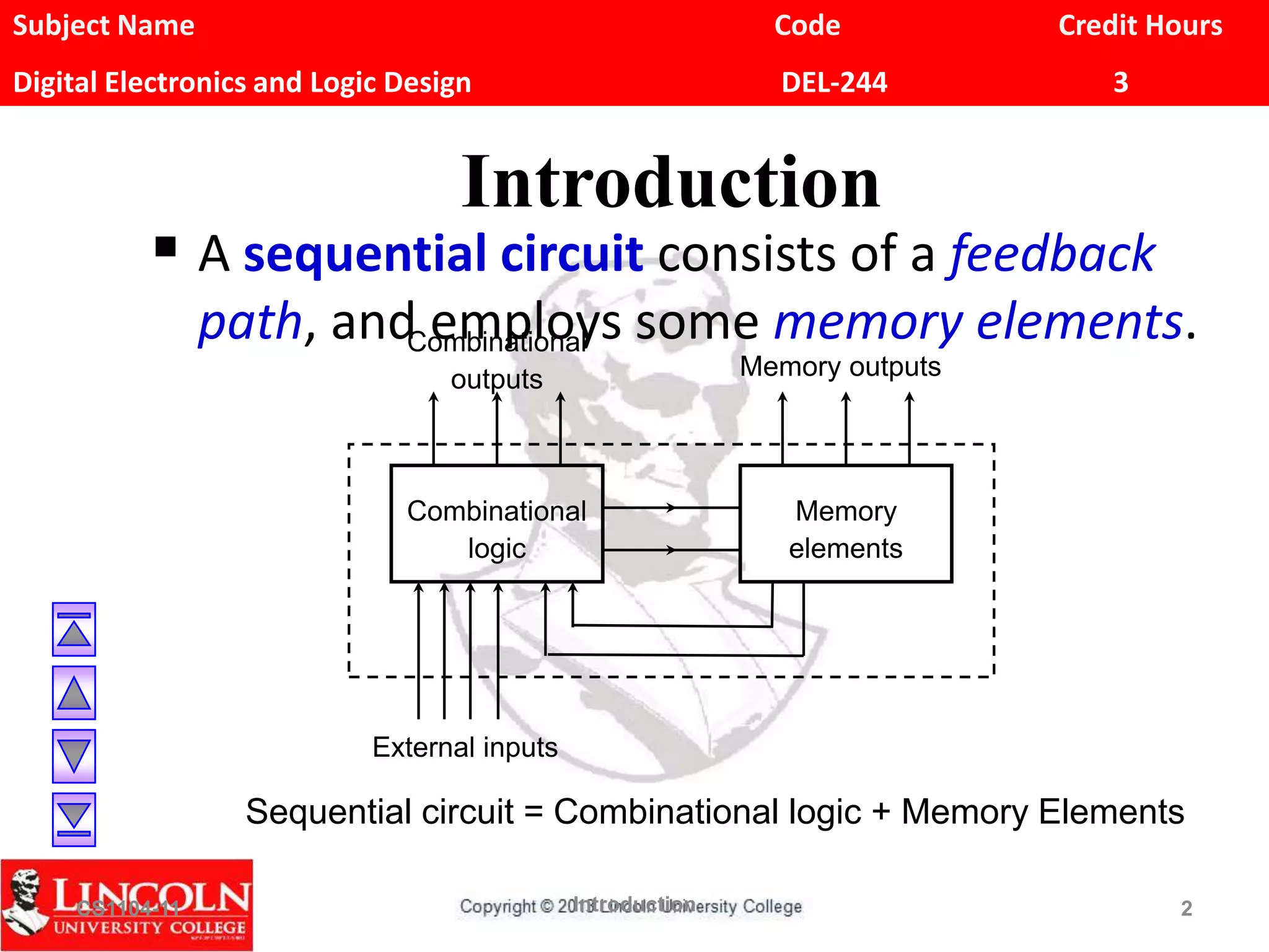
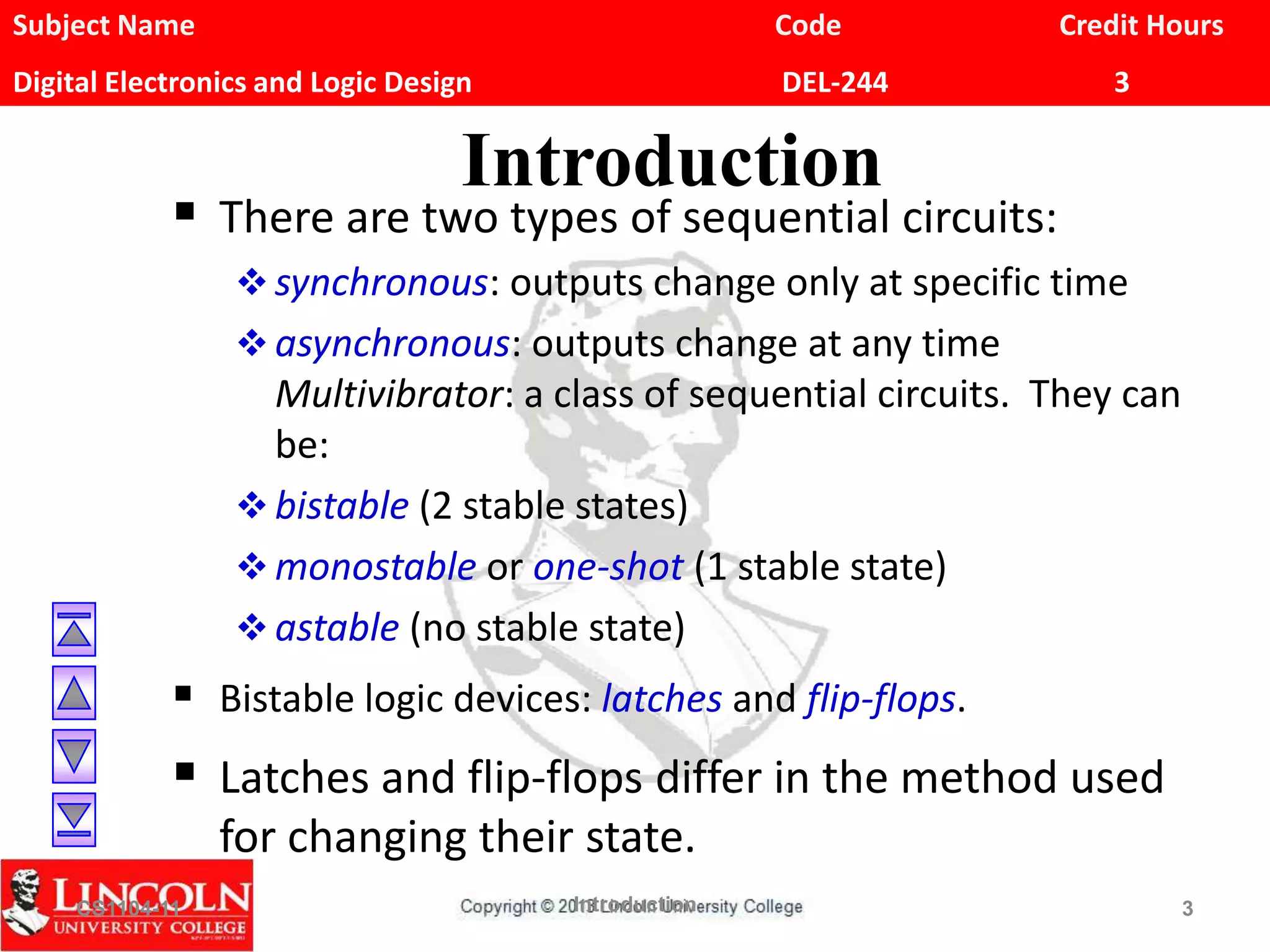
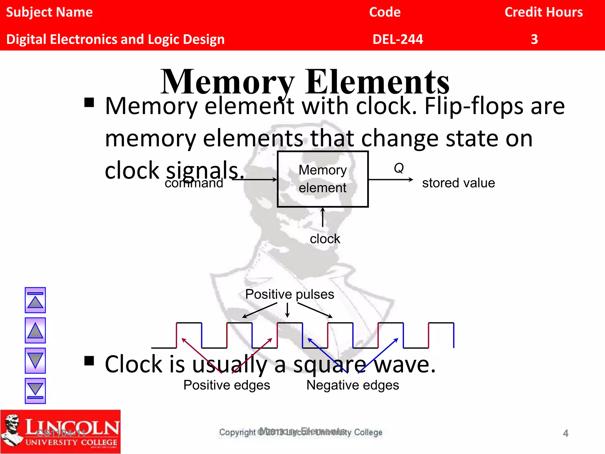
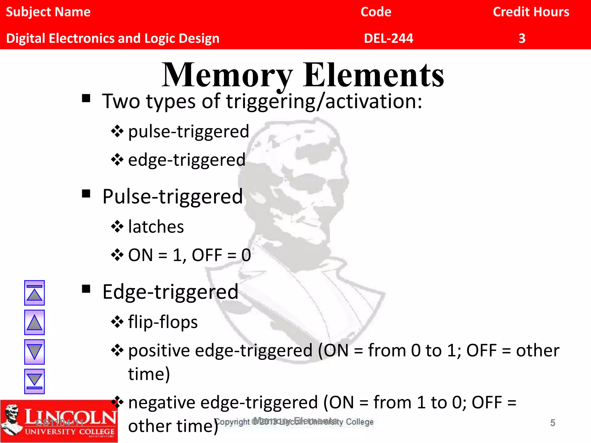
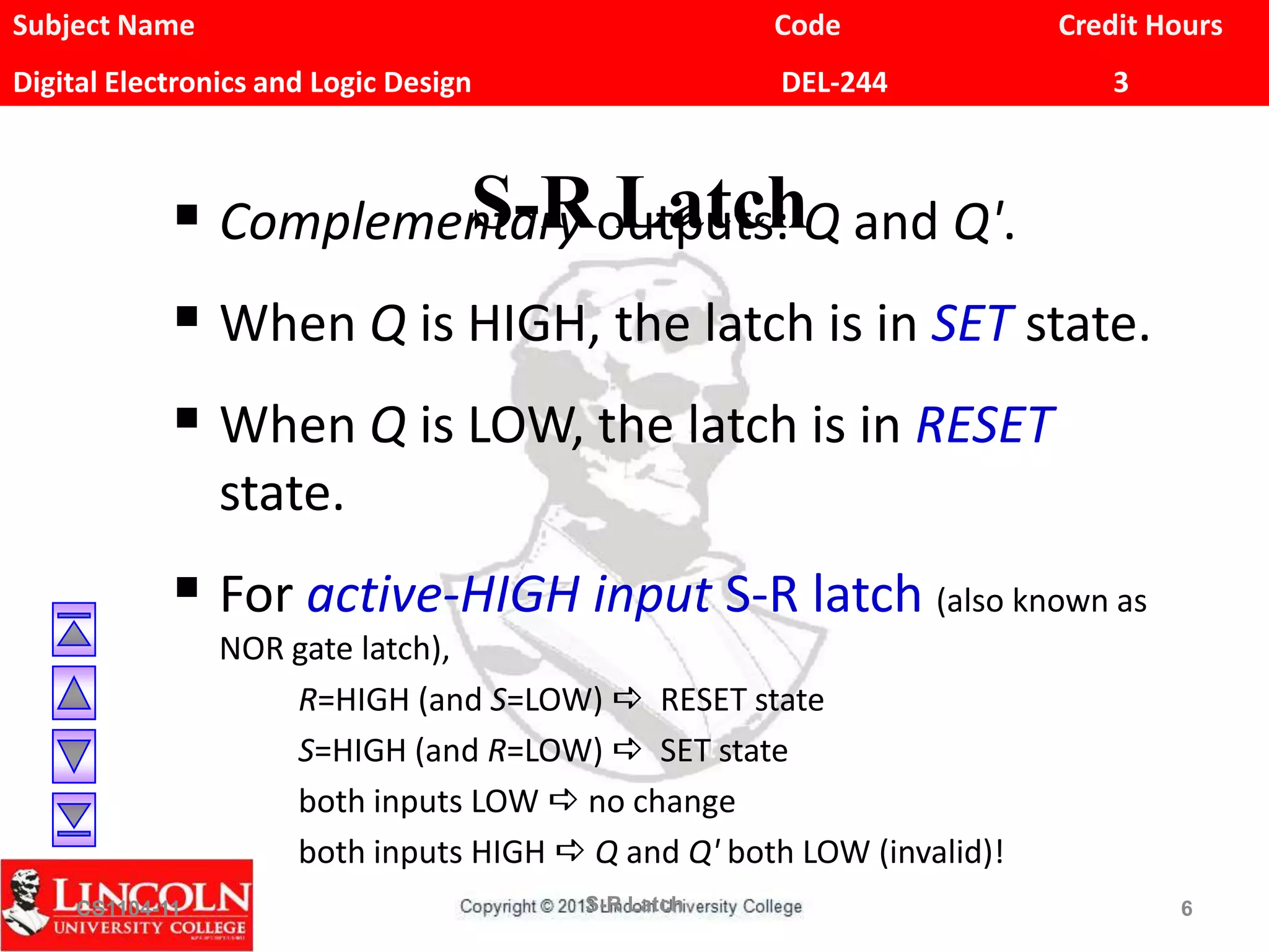
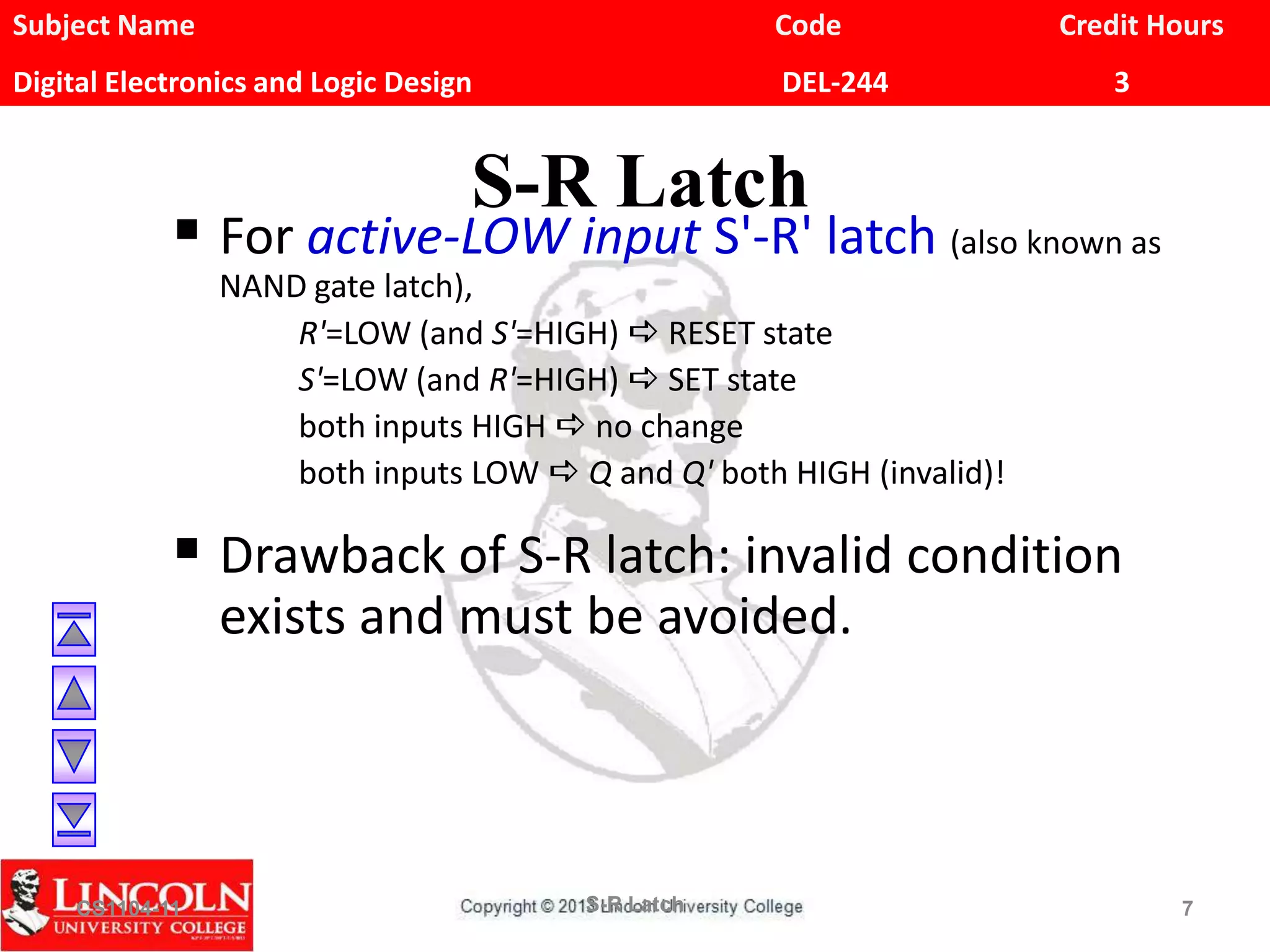
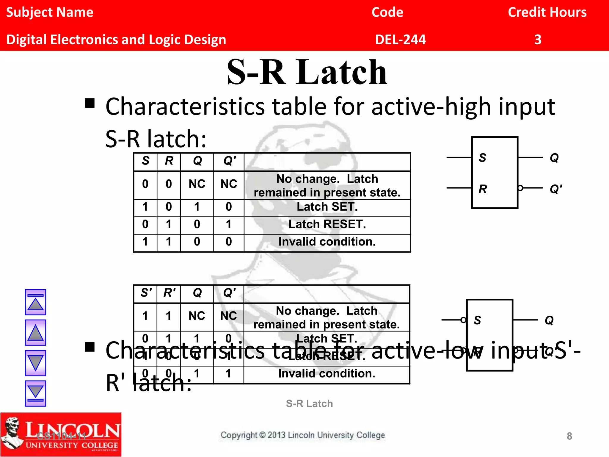
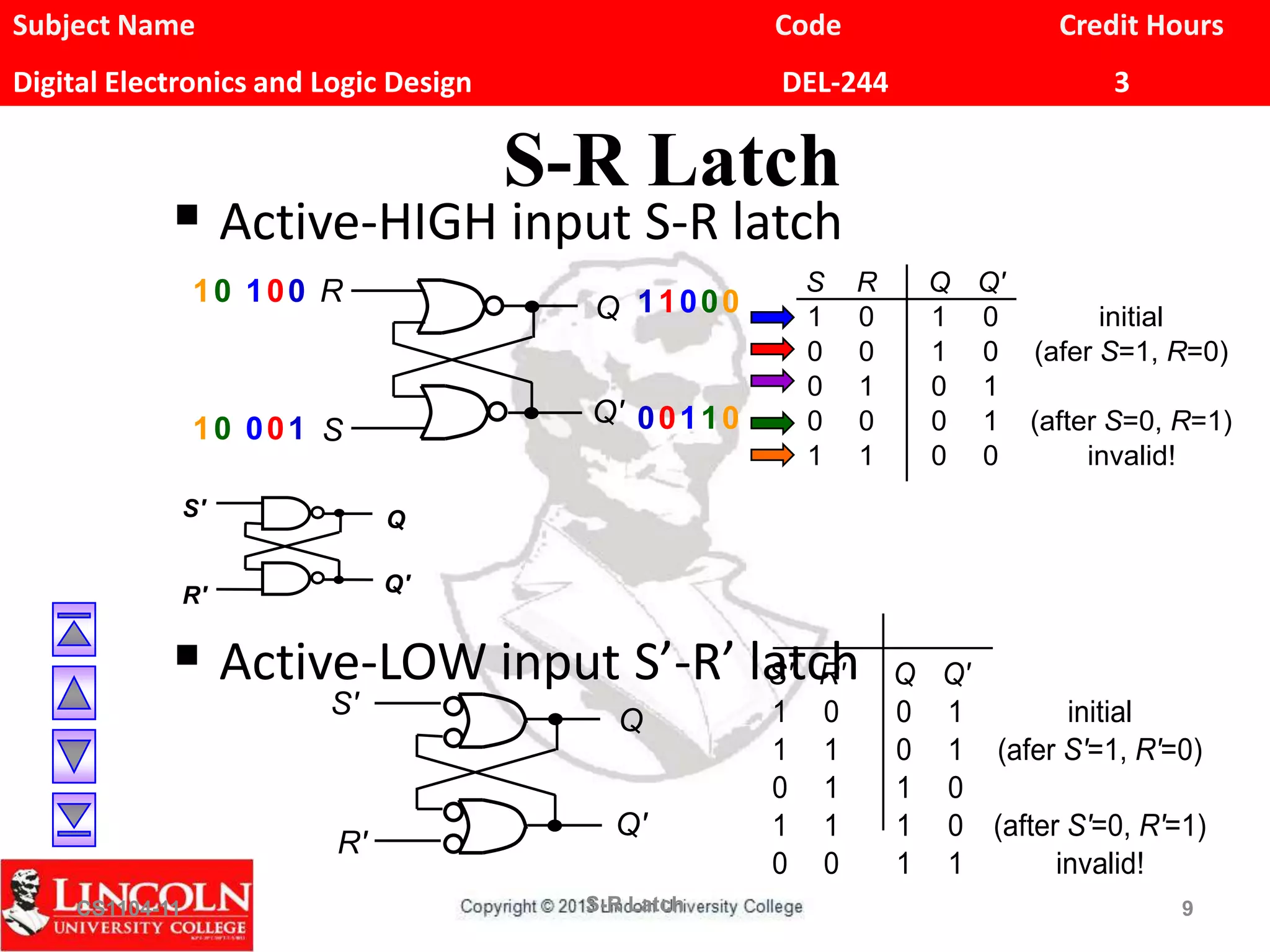
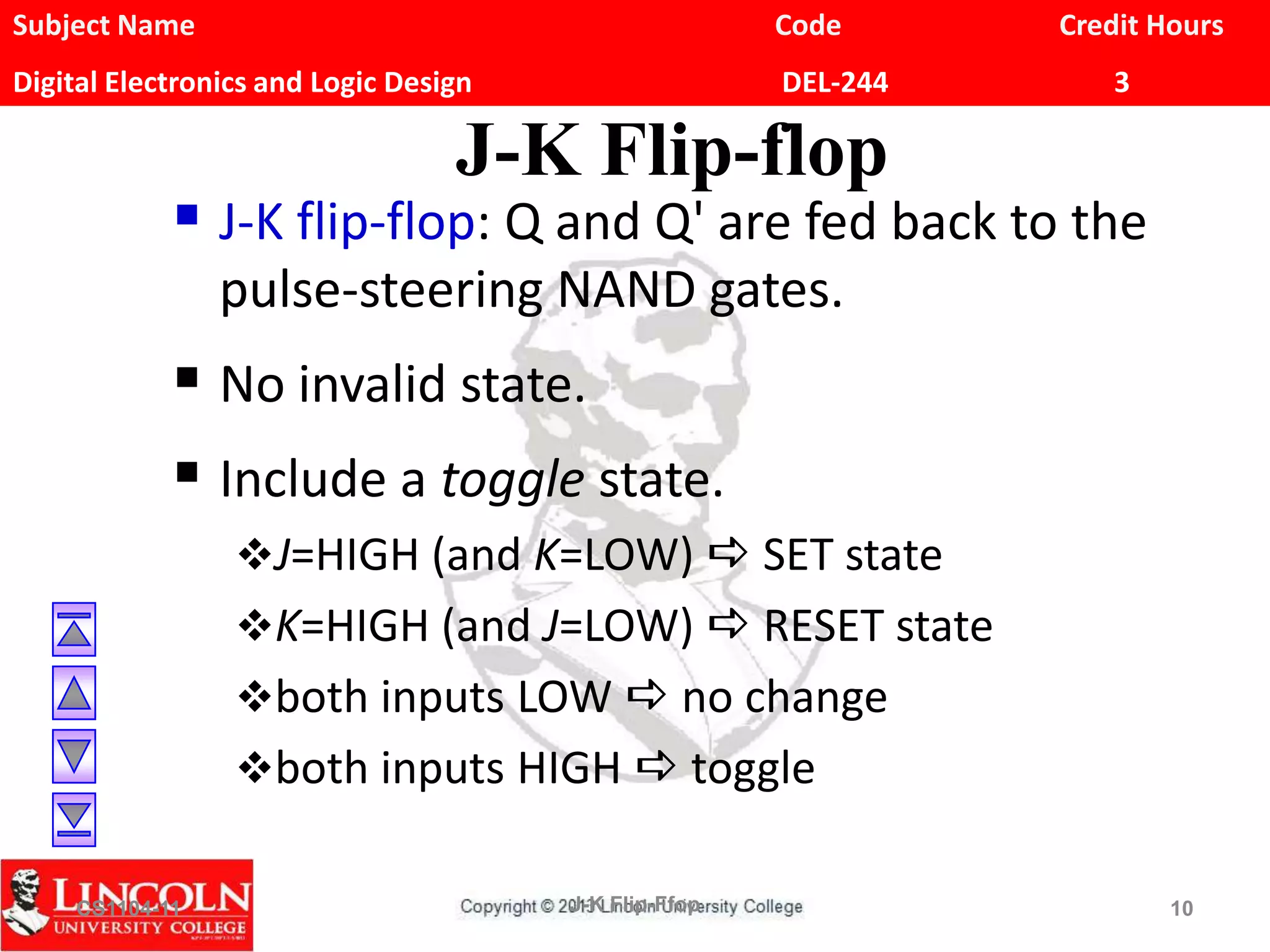
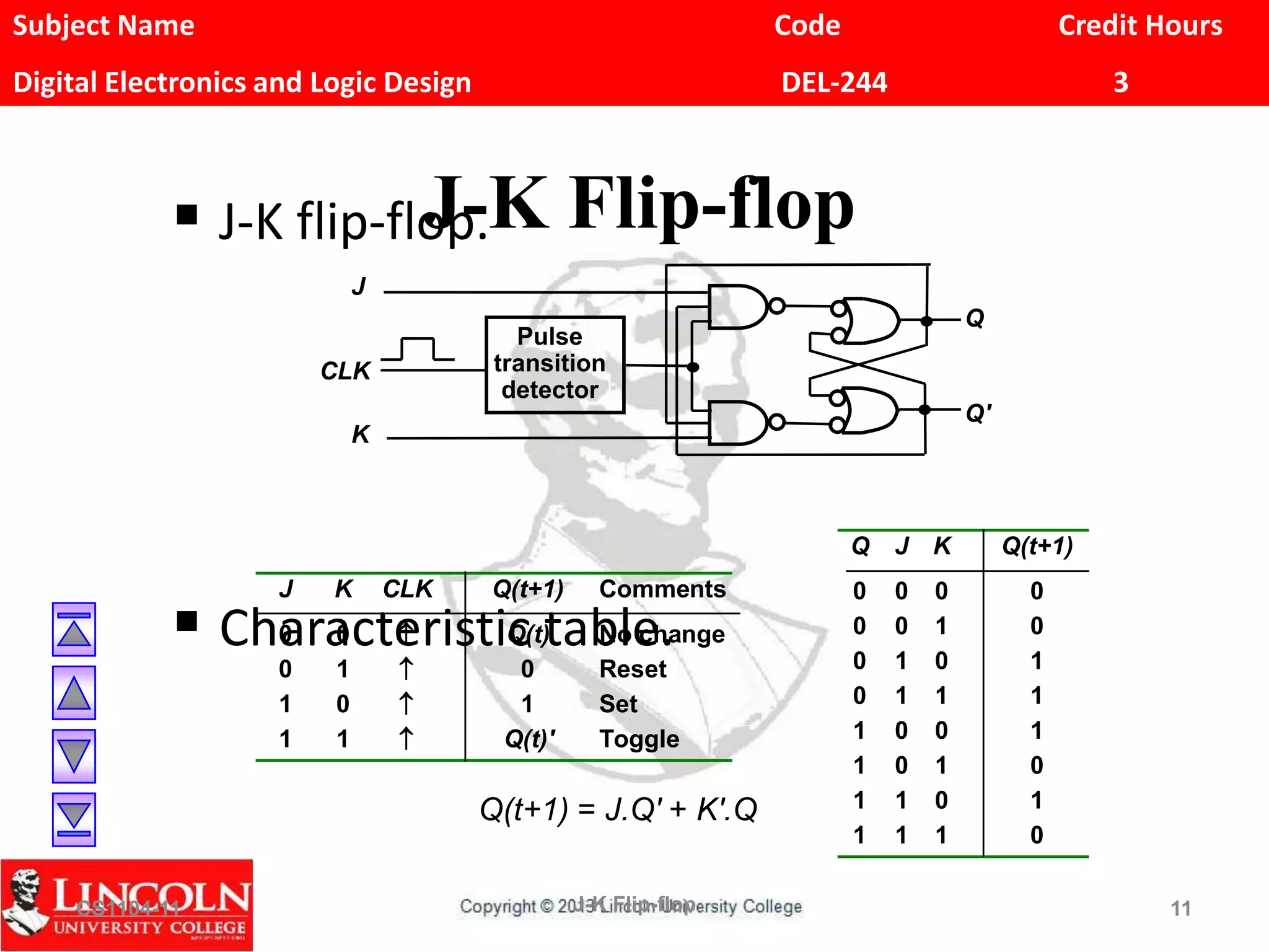
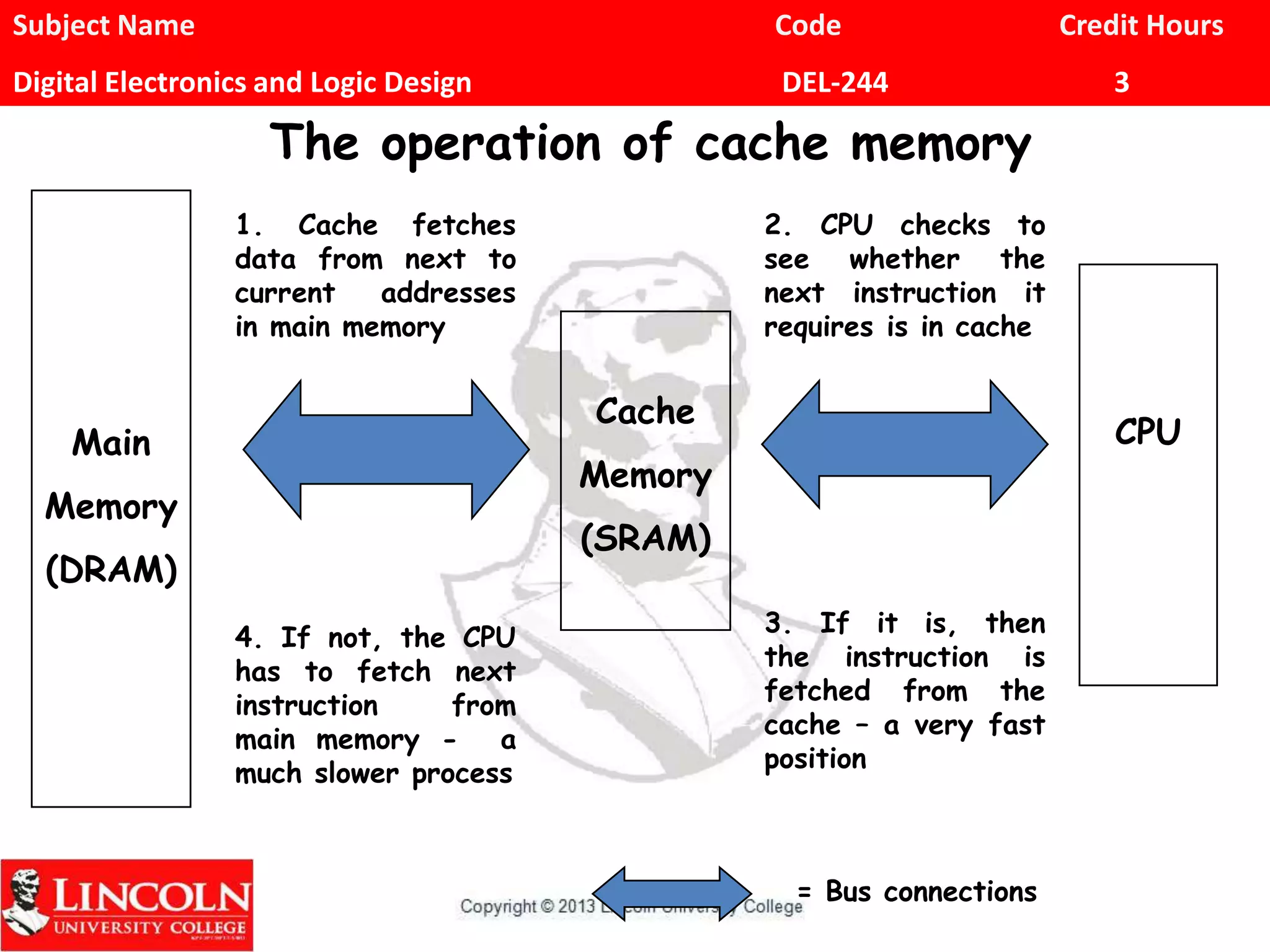
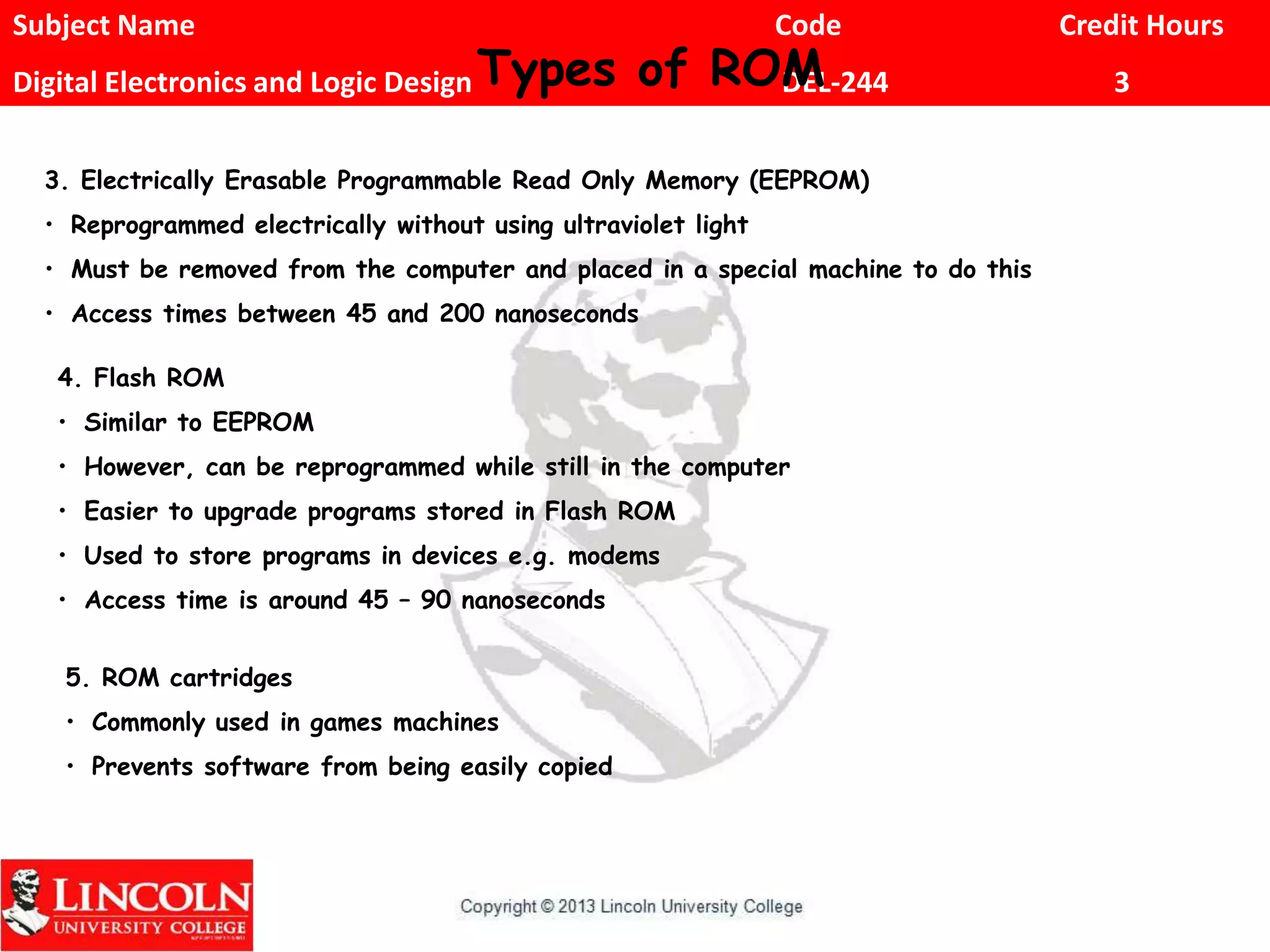

This document discusses sequential logic circuits and memory elements. It begins by introducing latches and flip-flops as basic memory elements in sequential circuits. It then describes different types of latches and flip-flops in more detail, including their structure, operation, and truth tables. The document also provides an overview of different types of computer memory, including RAM, ROM, cache memory, and virtual memory. It explains the basic characteristics and uses of each memory type.