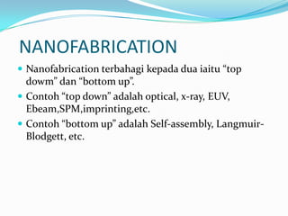
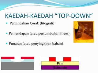
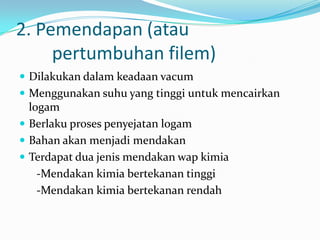
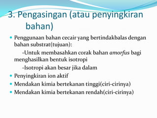
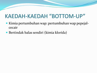
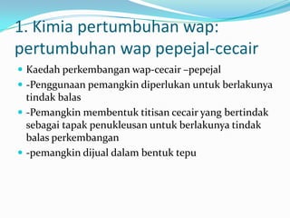
This document summarizes several nanofabrication technologies including buckyballs, carbon nanotubes, and methods for producing carbon nanotubes. Specifically, it discusses buckyballs being spherical carbon molecules and carbon nanotubes being long carbon tubes that can have conducting or semiconducting properties. It then describes three main production methods for carbon nanotubes: laser evaporation, carbon arc techniques, and chemical vapor deposition.
Fabrication methods - Nanoscience and nanotechnologiesNANOYOU
An introduction to fabrication methods.
This chapter is part of the NANOYOU training kit for teachers.
For more resources on nanotechnologies visit: www.nanoyou.eu
The document discusses electron beam lithography (EBL) for nano fabrication. EBL uses an electron beam to directly write nanoscale patterns on a resist-coated substrate. It allows for very high resolution down to 5 nm but has low throughput as it is a serial writing process. The key components of an EBL system include an electron gun, electron column for beam shaping and focusing, mechanical stage, wafer handling system, and control computer. EBL resists like PMMA can achieve high resolution but have limitations in sensitivity, etch resistance and thermal stability. EBL is widely used for research applications and mask making due to its high resolution, though it is too slow for high-volume manufacturing.
This document discusses various methods for synthesizing nanomaterials, including top-down and bottom-up approaches. The top-down approach involves breaking down bulk materials into nanoparticles, using methods like attrition and lithography. The bottom-up approach involves building nanoparticles from molecular precursors using methods like pyrolysis, solvothermal processes, and sol-gel techniques. These synthetic methods allow for the production of nanomaterials with applications in areas like drug delivery, coatings, and imaging. Further development could improve biological imaging and cancer treatment.
Nanotechnology involves working with materials at the nanoscale, between 1 to 100 nanometers. There are top-down and bottom-up approaches to creating nanoparticles. Top-down involves breaking bulk materials into nanoparticles while bottom-up involves building nanoparticles from individual atoms or molecules. Nanoparticles can be created through various methods including attrition, pyrolysis, and liquid phase techniques like sol-gel and microemulsions. Nanoparticles find applications in areas like batteries and 3D printing.
The sol-gel method involves creating an inorganic network through the formation and gelation of a colloidal suspension. Metal alkoxides and chlorides react with water through hydrolysis and polycondensation reactions to form this network. The sol-gel process is used to create protective coatings, thin films, fibers, and nano-scale powders for opto-mechanical applications and offers advantages over conventional glass production like low temperature operation and better control over material properties at the nano-scale.
This document provides an overview of nanotechnology. It defines nanotechnology as the study and engineering of matter at the nanoscale, or atomic level. The document outlines the history of nanotechnology from its conception in 1959 to modern applications. Key tools used in nanotechnology like atomic force microscopes and carbon nanotubes are described. The document also discusses different approaches (top-down vs bottom-up), materials used, and applications of nanotechnology in areas like drugs, fabrics, electronics, and computers. It provides examples of how nanotechnology is enhancing performance in these domains.
This document discusses Croatia's approach to integrating information and communication technologies (ICT) into its national school curriculum. It describes a bottom-up and top-down approach. The bottom-up approach involves getting individual teachers interested and trained in using ICT, while the top-down approach implements ICT on a national scale through policy decisions. The Croatian Academic and Research Network (CARNet) has played a key role in both approaches through various projects to provide infrastructure, training, and support to educational institutions. The ultimate goal is to transform schools into "digitally mature" environments that can fully utilize and benefit from ICT.
ISO 10993 Series Part 1: Evaluation and Testing In The Risk Management ProcessNAMSA
ISO 10993 Series Part 1: Evaluation and Testing In The Risk Management Process discusses what ISO 10993-1 addresses, as well as the general principles governing the biological evaluation of medical devices within a risk management process.
This document discusses InAs nanowire growth and characterization. It covers substrate preparation and control of catalyst size and position to influence nanowire properties. Growth dynamics are investigated using in-situ X-ray diffraction during growth interruptions. Novel SiO2 substrates are shown to alter surface diffusion and enable X-ray studies of individual nanowires. High resolution TEM images provide insights into growth mechanisms and parasitic growth. In conclusion, substrate fabrication allows control over nanowire positioning and properties, while in-situ studies provide insights into growth kinetics.
WHO SHOULD ATTEND?
Technicians, engineers, and researchers.
Decision makers, policy makers, and managers.
INTRODUCTION
This course focuses on the major process technologies used in fabrication of integrated circuits (ICs), discrete, and other semiconductor devices, which includes light emitting diodes (LEDs). Each topic covers important scientific aspects of wafer processing steps, which include crystal growth and wafer preparation, crystal defects and purification techniques, contamination control, oxidation, diffusion, ion implantation, lithography, thin film deposition technology, etching, metallization, process integration, electronic packaging and yield.
LEARNING OUTCOMES
Upon completion of this course, participants will be able to:
i. Explain processes of developing semiconductor devices with various architectures.
ii. Understand types of operations sequence in fabricating a typical device.
iii. Calculate important parameters applicable to different individual process steps.
iv. Distinguish and compare different types of techniques used in different individual process steps.
v. Propose and design a simple semiconductor-device fabrication process flow.
A Biological Smart Platform for the Environmental Risk AssessmentDavide Nardone
This document describes a biological smart platform for environmental risk assessment. It consists of sensors that collect data, a Web of Things platform, and a web application. The data is analyzed using fuzzy inference systems and machine learning techniques. The goals are to assess environmental risks both qualitatively and quantitatively and visualize the information for users. The platform uses a multi-tier architecture with things, connectivity layers, a global infrastructure cloud, and applications. Data is ingested using Apache Kafka and Spark Streaming and stored in the cloud. The web application provides a cross-platform interface for users to access the risk assessments.
This document discusses the brewing process and history of beer production. It begins by defining breweries and noting the oldest brewery is the Weinhnstephan brewery in Germany. It then covers the industrialization of breweries dating back 5000 years, and major technological advances like refrigeration and understanding of microbes. The modern brewing process uses stainless steel vessels and precise temperature control. Beer is made from water, starch sources like malted barley, hops, and yeast through a multi-step process including mashing, boiling, fermenting and packaging.
This document discusses different approaches for nanofabrication including top-down and bottom-up. It describes various synthesis methods for nanoparticles including solid, liquid, and gas phase techniques. Specific solid phase methods like agitated ball milling and specific liquid phase techniques like sol-gel synthesis and solvothermal synthesis are explained. Gas phase methods like chemical vapor deposition, laser ablation, and references for further reading are also summarized.
Nanotechnology refers to the manipulation of matter at the atomic and molecular scale. It promises faster, smaller, and more energy efficient computers through the use of carbon nanotubes to replace silicon transistors. This could lead to computers that are twice as fast but half the size within the next decade. Other applications of nanotechnology in computing include using quantum dots for quantum computing, DNA logic gates for DNA computing, and non-volatile RAM to allow for more portable devices without backup batteries. Overall, nanotechnology has the potential to revolutionize computing through the development of new nanomaterials and fabrication techniques at the atomic scale.
Graphene Syntheis and Characterization for Raman Spetroscopy At High PressureNicolasMORAL
This document summarizes Nicolas Moral's thesis on synthesizing and characterizing single- and double-layer graphene using two methods under high pressure conditions. The first method deposits graphene flakes onto silicon dioxide substrates using mechanical exfoliation, while the second uses free-standing graphene grown on a copper grid. Both methods allow for optical identification and Raman spectral confirmation of graphene layers. While characterization is complete, challenges remain in reliably transferring the graphene samples for high pressure experiments.
Techniques for synthesis of nanomaterials (II) shubham211
This document discusses various techniques for liquid phase synthesis and mechanical synthesis of nanomaterials. It begins by outlining five major categories of liquid phase synthesis: colloidal methods, sol-gel processing, microemulsions, hydrothermal synthesis, and the polyol method. It then describes specific methods such as colloidal precipitation, sol-gel techniques using metal alkoxide precursors, and applications of sol-gel processing for ceramics and coatings. Mechanical synthesis methods covered include high-energy milling, mechanical alloying, severe plastic deformation techniques like equal channel angular pressing and high-pressure torsion.
The document discusses the ball milling method for producing nano materials. It involves using a ball mill, which rotates around a horizontal axis partially filled with the material to be ground plus grinding media like balls. The balls crush the solid material into nano crystallites due to the gravity and kinetic forces as they rotate at high energy inside the container. Some examples given are using ball milling to produce carbon nanotubes, boron nitride nanotubes, metal oxide nano crystals like cerium oxide and zinc oxide. Ball milling of graphite can also produce nanostructured graphite for hydrogen storage applications.
The document discusses nanomaterial synthesis methods. It begins with an introduction to nanotechnology and challenges in the field. It then covers bottom-up and top-down approaches to nanomaterial synthesis. Specific synthesis methods covered include evaporation and condensation growth, lithography technology, and methods for creating nano-composites. A variety of nanoparticle synthesis techniques are also discussed.
Nano Material
Introduction and Synthesis
Nanomaterials describe, in principle, materials of which a single unit is sized (in at least one dimension) between 1 and 1000 nanometres (10−9 meter) but is usually 1—100 nm (the usual definition of nanoscale[1]).
Nanomaterials research takes a materials science-based approach to nanotechnology, leveraging advances in materials metrology and synthesis which have been developed in support of microfabrication research. Materials with structure at the nanoscale often have unique optical, electronic, or mechanical properties.
Nanomaterials are slowly becoming commercialized[2] and beginning to emerge as commodities.[3]
This document discusses various techniques for synthesizing nanoparticles, including sol-gel synthesis, colloidal precipitation, co-precipitation, combustion technique, hydrothermal technique, high energy ball milling, and sonochemistry. It provides details on specific methods like the Frens method for synthesizing gold nanoparticles, co-precipitation reaction for iron oxide nanoparticles using FeCl3 and benzene tetracarboxylic acid, combustion synthesis using lithium nitrate and bismuth nitrate with urea and glycerol, and hydrothermal treatment for titanium dioxide nanoparticles. The advantages of these techniques in producing nanoparticles at low temperatures and with good control of properties are highlighted.
The document discusses different methods for synthesizing nanomaterials, including top-down and bottom-up approaches. It describes growth kinetics involving cluster formation, nucleation, and growth. Bottom-up synthesis techniques include physical vapor deposition methods like evaporation and sputtering, as well as chemical methods like wet chemical synthesis, microemulsions, and colloidal synthesis. Nucleation can be homogeneous or heterogeneous, and supercooling affects nucleation rate and crystal size. Overall the document provides an overview of the various techniques used for controlling size, shape, structure, and properties during nanomaterial synthesis.
The sol-gel technique involves creating a sol by dispersing colloidal particles in a liquid. This sol is then used to deposit coatings on substrates via spraying, dipping, or spinning. The particles in the sol are polymerized to form a continuous gel network. Finally, heat treatment forms an amorphous or crystalline coating. This technique allows for highly pure and uniform products to be formed at low temperatures and is used to create materials for applications like capacitors, transparent semiconductors, glasses, lenses, and nanopowder for dental and biomedical uses.
The document provides an overview of various lithography techniques including photolithography, electron beam lithography, nanolithography, X-ray lithography, AFM nanolithography, soft lithography, nanoimprint lithography, and dip-pen nanolithography. It discusses the basic principles, steps involved, advantages, and applications of each technique for fabricating nanostructures.
The document provides an overview of chemical vapor deposition (CVD) and physical vapor deposition (PVD) processes. CVD involves reacting vapor phase chemicals in a chamber to form a thin solid film on a substrate. It can be used to deposit a variety of materials. PVD involves physically vaporizing a material in a chamber and re-depositing it as a thin film on a substrate. It has various variants like sputtering and evaporative deposition. Both CVD and PVD are used to deposit thin films for applications like semiconductor devices, coatings, optical fibers and composites.
This document provides an overview of occupational safety and health, including definitions, goals, and key aspects. It discusses occupational safety and health programs and industrial hygiene programs. It also describes common workplace hazards like physical/mechanical hazards, chemical hazards, biological hazards, noise hazards, temperature extremes, electricity, and more. Specific industries like construction, agriculture, mining, and services sectors are reviewed in terms of their occupational health and safety challenges. The document also summarizes occupational health and safety in India, including constitutional provisions, national policies, and key legislation like the Factories Act.
2. NANOFABRICATION
Nanofabrication terbahagi kepada dua iaitu “top
dowm” dan “bottom up”.
Contoh “top down” adalah optical, x-ray, EUV,
Ebeam,SPM,imprinting,etc.
Contoh “bottom up” adalah Self-assembly, Langmuir-
Blodgett, etc.
4. 1. Pemindahan Corak (litografi)
Menambah satu bahan yang sensitif kepada cahaya yang
dipangil photoresist kepada permukaan bahan substrat
Meletakan photomask selari dengan bahan substrat
Pengunaan photomask adalah untuk menentukan bahagian-
bahagian terkena pancaran UV atau tidak
-Diperbuat daripada kaca atau kuarza dengan corak krom
- Walaupun topeng perlu dibuat dengan litografi
Dengan itu bahagian yang terkena sinaran UV akan
“membentuk”
Terdapat dua jenis photoresists
-positive resists
-negative resists
5. 2. Pemendapan (atau
pertumbuhan filem)
Dilakukan dalam keadaan vacum
Menggunakan suhu yang tinggi untuk mencairkan
logam
Berlaku proses penyejatan logam
Bahan akan menjadi mendakan
Terdapat dua jenis mendakan wap kimia
-Mendakan kimia bertekanan tinggi
-Mendakan kimia bertekanan rendah
6. 3. Pengasingan (atau penyingkiran
bahan)
Penggunaan bahan cecair yang bertindakbalas dengan
bahan substrat(tujuan):
-Untuk membasahkan corak bahan amorfus bagi
menghasilkan bentuk isotropi
-Isotropi akan besar jika dalam
Penyingkiran ion aktif
Mendakan kimia bertekanan tinggi(ciri-cirinya)
Mendakan kimia bertekanan rendah(ciri-cirinya)
8. 1. Kimia pertumbuhan wap:
pertumbuhan wap pepejal-cecair
Kaedah perkembangan wap-cecair –pepejal
-Penggunaan pemangkin diperlukan untuk berlakunya
tindak balas
-Pemangkin membentuk titisan cecair yang bertindak
sebagai tapak penukleusan untuk berlakunya tindak
balas perkembangan
-pemangkin dijual dalam bentuk tepu
9. 2. Bertindak balas sendiri (kimia
klorida)
Berlaku pemanasan sendiri kerana bertindak balas
dengan ion lain.
Hasil daripada tindak balas terhasilah substrak
Klorida: merujuk kepada keadaan Pecah Sempadan
dalam satu-satu larutan.
Contoh bahan-bahan yang biasanya berlaku koloid:-
- Krim putar
- Susu
- Kabus
- Asap
10. SIAPAKAH ANTARA ORANG YANG
TERAWAL YANG MENKAJI TENTANG
NANOFABRICATION
Byron D. Gates
Declan Ryan
Qiaobing Xu
Michael D. Stewart
C. Grant Willson