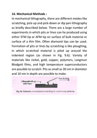
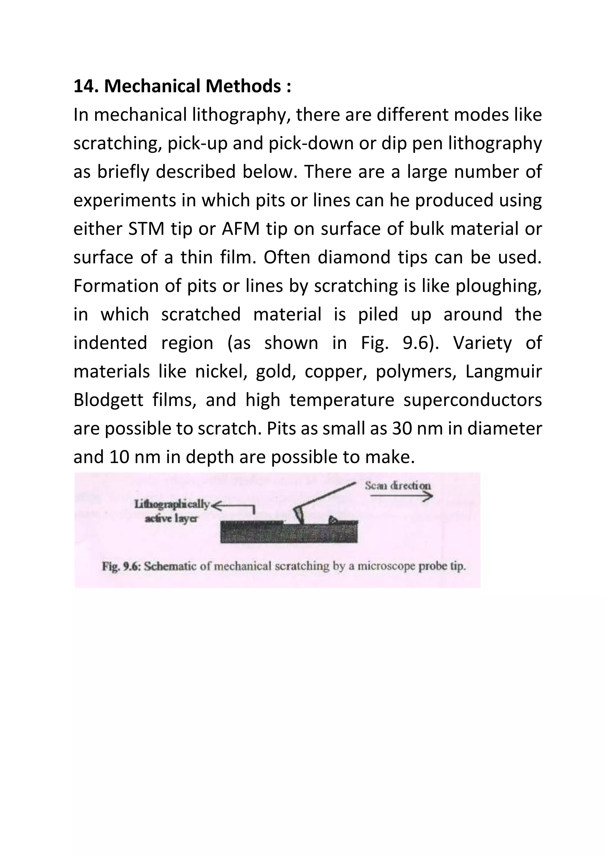
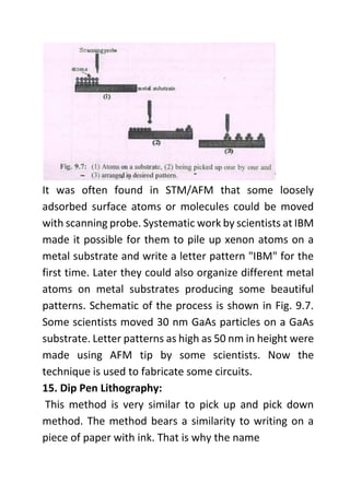
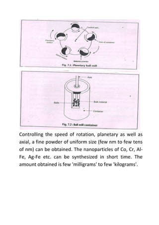
14. Mechanical Methods :
In mechanical lithography, there are different modes like
scratching, pick-up and pick-down or dip pen lithography
as briefly described below. There are a large number of
experiments in which pits or lines can he produced using
either STM tip or AFM tip on surface of bulk material or
surface of a thin film. Often diamond tips can be used.
Formation of pits or lines by scratching is like ploughing,
in which scratched material is piled up around the
indented region (as shown in Fig. 9.6). Variety of
materials like nickel, gold, copper, polymers, Langmuir
Blodgett films, and high temperature superconductors
are possible to scratch. Pits as small as 30 nm in diameter
and 10 nm in depth are possible to make.
It was often found in STM/AFM that some loosely
adsorbed surface atoms or molecules could be moved
with scanning probe. Systematic work by scientists at IBM
made it possible for them to pile up xenon atoms on a
metal substrate and write a letter pattern "IBM" for the
first time. Later they could also organize different metal
atoms on metal substrates producing some beautiful
patterns. Schematic of the process is shown in Fig. 9.7.
Some scientists moved 30 nm GaAs particles on a GaAs
substrate. Letter patterns as high as 50 nm in height were
made using AFM tip by some scientists. Now the
technique is used to fabricate some circuits.
15. Dip Pen Lithography:
This method is very similar to pick up and pick down
method. The method bears a similarity to writing on a
piece of paper with ink. That is why the name
dip pen lithography is given. An AFM tip is used as a pen
and molecules are used as ink (see Fig. 9.8). Appropriate
molecules picked up by the tip from the source of
molecules can be transported and transferred at desired
place on the substrate. Letters with line thickness as small
as 15 nm and distance 5 nm have been written.
Overwriting and erasing capability of dip pen lithography
is quite a unique feature.
16. Optical Scanning Probe Lithography: As discussed
earlier, very high resolution ~20-50 nm is possible,
overcoming the diffraction limit, even with visible light
using Scanning Near-Field Optical Microscope (SNOM).
This is attributed to near-field component of
electromagnetic radiation. In SNOM (see Fig. 9.9), a fine
spot of visible light emerging through an aperture, scans
on the surface at a distance of ~λ / 50, where ) is the
wavelength of light used for scanning. By placing the
aperture close to the photoresist coated substrate, it is
possible to obtain as small as ~50 nm size features
routinely.
17. Thermo-Mechanical Lithography:
It is also possible to use an AFM tip along with a laser
beam and carry out nanolithography (see Fig. 9.10).
While the AFM-tip is in contact with coating like PMMA,
laser beam strikes the same point of the coating. This
heats the film locally enabling the tip to penetrate in the
material and make a pit. This thermo-mechanical method
is capable of producing resolution as high as ~30 nm.
18. Electrical Scanning Probe Lithography:
In this method, as illustrated in Fig. 9.11, a voltage is
applied between the STM tip and the sample. Above
some critical voltage if large current flows between the
tip and the sample, an irreversible change can occur in
sample surface. Variety of bulk solid and thin films
surfaces has been patterned using this method. In silicon
or modified silicon surfaces, –30-60 nm wide and –5-10
nm deep lines have been engraved.
19 SOFT LITHOGRAPHY
There are some inexpensive, non-conventional
techniques that have been developed, useful for
patterning non-planer and non-routine, inorganic,
organic, biological samples. By conventional techniques
we mean techniques like photon lithography or particle
lithography. To achieve resolutions better than 100 nm
feature size, X-rays, electrons or ions need to be used in
conventional lithography. Due to various technical
problems related to radiation and matter interactions,
expensive and sometimes dedicated instruments using
high energy beams are required. These are indeed used
in microelectronics industry. However for other
purposes, soft lithography is a useful alternative to obtain
Fig. 9.12: Process of making master: (1)A desired pattern
is obtained on silicon substrate using suitable
lithography. (2) Prepolymer is poured on silicon-
patterned substrate. (3) After proper heat treatment
master is removed easily from silicon pattern and is ready
for use.
resolution better than ~100 nm at low cost. Moreover,
the method is applicable from few nm to few um size
features. The name soft lithography is used to mean the
techniques using materials like polymers, organic
materials or self assembled films. In general soft
lithography technique involves fabrication of a patterned
master, molding of master and making replicas. A master
is usually made using X-ray or electron beam lithography.
It is supposed to be quite rigid. A mold is usually made
using a polymer-like polydimethylsiloxane (PDMS),
epoxide, polyeurethane etc. PDMS is most common
amongst the polymers used for molding due to its
attractive properties-like thermal stability (~150 °C),
optical transparency, flexibility (~160% elongation),
capability of cross-linking using IR or UV radiation etc.
However during molding some distortions can take place
and adequate control has to be practiced to achieve
reproducible and rbquired results. Figure 9.12 illustrates
the method of making a master. Replication of patterns
can be done by different ways, the most common are as
described below.
20. Microcontact Printing (µCP)
A PDMS stamp is dipped in an alkanethiol solution (see
Fig. 9.13) and pressed against the metallized (Au, Ag, Cu)
substrate. Those parts of substrate, which come in
contact with the PDMS, receive layers of alkanethiol. The
monolayers do not spread on the substrate. Further,
these self assembled monolayers can be used as resists
for selective etching or deposition. The printing being
simultaneous, it is a fast method.
22. Replica Molding (REM)
In this method, a PDMS master or stamp is used to
replicate a number of copies. For example a solution of
polyurathene (see Fig. 9.14) is poured in
Fig.
9.14: Replica molding: (1) PDMS master, (2) pour a
prepolymer on master, and (3) after heat treatment
pattern (its complementary part) is transferred into
polymer.
PDMS and cured using UV light or thermal treatment so
that polyurathene becomes solid. PDMS can be easily
removed so that a pattern opposite to that is produced in
polyurathene. By applying small pressure on PDMS, it is
possible to further reduce the size of the features smaller
than in the original pattern. Nanostructures ~30 nm have
been achieved using this method.
23. Micro Transfer Molding (µTM)
As shown in Fig. 9.15, a pre-formed polymer is poured in
PDMS stamp. Excess polymer is removed by blowing
nitrogen gas on it and the stamp is pressed against a
substrate. Using thermal treatment polymer is imprinted
on the substrate and mould is removed.
Fig.9.15:Microtransfer molding: (1) Prepolymer poured
on the stamp, (2) Excess solution is removed using
nitrogen blow, (3) Stamp is pressed on the substrate and
cured for one hour, and (4) Stamp removed carefully.
24. Micromolding in Capillaries (MIMIC) -In this
technique (see Fig. 9.16) a PDMS stamp is placed on a
substrate to be patterned. A low viscosity polymer is then
placed in contact with PDMS. The
Fig. 9.16: Micromolding in capillaries: (1) put the stamp
over substrate, (2) pour the solution from open channel
and cure it, and (3) stamp is removed and the pattern
remains on substrate.
liquid flows into channels of PDMS by capillary action.
After thermal treatment of curing with UV radiation the
polymer gets solidified. PDMS stamp is then removed to
obtain patterned substrate.
25. Solvent-Assisted Micromolding (SAMIM)
A PDMS stamp coated with a solvent is pressed against
the substrate coated with a polymer film (see Fig. 9.17).
Solvent softens the polymer surface in
Fig. 9.17: Solvent assisted micromolding: (1) prepare a
thin film on substrate, (2) put the solvent coated stamp
over substrate and (3) mold is removed after evaporating
the solvent.
contact. PDMS can be removed after solvent has
evaporated. PDMS stamp itself is not affected by the
solvent. Volatile and substrate dissolving solvents, but
not PDMS stamp dissolving, need to be used. Often
Novalac' coating is given to the substrates.
Polymethylmethacrylate (PMMA), cellulose acetate,
polyvinyl chloride etc. are used as polymers.
26. Nanoimprint lithography
Although soft lithography techniques are fast,
economically useful and in principle capable of producing
sub-nanometer patterns, the mechanical stability of such
stamps is often a problem. Keeping good contact
between the substrate and the mould also is often
problematic. Various further treatments of PDMS
surface, use of shadow masks and .proper choice of
chemicals (solvents or organic molecules) etc. are
necessary to achieve very high resolution and quality
patterns. The field is yet under development and no
unique method is so far available.
1.3,Preparation Techniques:- As it has been discussed
earlier, the physical properties of material change
drammatically when they are reduced to nanoscale. The
process by which the nanoscale particles are obtained is
termed as 'nano-fabrication' or 'nanoscale
manufacturing' or 'synthesis'. For getting nanoparticles
one can start from a bulk material and can cut down to
the nanoscale. This particular type of nanofabrication is
called lop-down nanofabrication', because it starts with a
large structure and proceeded to make it smaller.
Conversely, starting with individual atoms and building
up a nanomaterial is called 'bottom-up nanofabrication'.
Large number of techniques are available to manufacture
(synthesis) different types of nanomaterials in different
forms i.e. colloids, cluster, poWder, thin films etc. There
are various physical, chemical, biological and hybrid
techniques to synthesize nanomaterials. The chart shows
different commonly used techniques. The technique -
selected is decided by the material of interest, type of
nanostructure, size, quality and quantity.
1.3.1 Physical Methods : Mechanical Method
High Energy Ball Milling : This is one of the simplest
methods of making nanoparticles of some metals and
alloys. This gives nanoparticles in powder form. This is
top-down nanofabrication where the material in powder
or flakes of dimensions less than 50 gm are reduced to
nanoparticles in powder form. The different types of mills
used are planetary, vibratory, rod etc. Usually one or
more containers are used and the container size depends
on the quantity of nanoparticles to be fabricated.
Hardened steel or tungsten carbide balls are put in
container along with powder or flakes of the bulk
material. The initial material is in bulk form and is of
arbitrary size and shape. The ratio of the balls and
material is 2 :1 and container should be less than half
filled as shown in Fig. 7.1. If the container is more than
half filled, the efficiency of milling reduces.
Use of large balls increases the impact energy on collision
and hence gives smaller grain size but produces larger
defects in the particles. In the process, some impurities
may be added from balls. The air present in the container
may also contaminate the nanoparticles. The whole
process is carried out in a tight lid container. The
containers are rotated at high speed around own axis. In
addition to this, they may be rotated around some
central axis and are called as 'planetary ball mill'. Due to
collisions, the temperature may rise from 100 to 1100°C,
but a lower temperature is faw - I! • the heat generated.
When the containers are rotating around the central axis,
the material is forced to the walls and is pressed against
the walls due to centrifugal force. But due to the motion
of containers around their own axis, the material is forced
to other region of the container as shown in Fig. 7.2.
Controlling the speed of rotation, planetary as well as
axial, a fine powder of uniform size (few nm to few tens
of nm) can be obtained. The nanoparticles of Co, Cr, Al-
Fe, Ag-Fe etc. can be synthesized in short time. The
amount obtained is few 'milligrams' to few 'kilograms'.

Nanotechnology-3.docx

  • 1.
    14. Mechanical Methods: In mechanical lithography, there are different modes like scratching, pick-up and pick-down or dip pen lithography as briefly described below. There are a large number of experiments in which pits or lines can he produced using either STM tip or AFM tip on surface of bulk material or surface of a thin film. Often diamond tips can be used. Formation of pits or lines by scratching is like ploughing, in which scratched material is piled up around the indented region (as shown in Fig. 9.6). Variety of materials like nickel, gold, copper, polymers, Langmuir Blodgett films, and high temperature superconductors are possible to scratch. Pits as small as 30 nm in diameter and 10 nm in depth are possible to make.
  • 2.
    It was oftenfound in STM/AFM that some loosely adsorbed surface atoms or molecules could be moved with scanning probe. Systematic work by scientists at IBM made it possible for them to pile up xenon atoms on a metal substrate and write a letter pattern "IBM" for the first time. Later they could also organize different metal atoms on metal substrates producing some beautiful patterns. Schematic of the process is shown in Fig. 9.7. Some scientists moved 30 nm GaAs particles on a GaAs substrate. Letter patterns as high as 50 nm in height were made using AFM tip by some scientists. Now the technique is used to fabricate some circuits. 15. Dip Pen Lithography: This method is very similar to pick up and pick down method. The method bears a similarity to writing on a piece of paper with ink. That is why the name
  • 3.
    dip pen lithographyis given. An AFM tip is used as a pen and molecules are used as ink (see Fig. 9.8). Appropriate molecules picked up by the tip from the source of molecules can be transported and transferred at desired place on the substrate. Letters with line thickness as small as 15 nm and distance 5 nm have been written. Overwriting and erasing capability of dip pen lithography is quite a unique feature. 16. Optical Scanning Probe Lithography: As discussed earlier, very high resolution ~20-50 nm is possible, overcoming the diffraction limit, even with visible light using Scanning Near-Field Optical Microscope (SNOM). This is attributed to near-field component of electromagnetic radiation. In SNOM (see Fig. 9.9), a fine spot of visible light emerging through an aperture, scans on the surface at a distance of ~λ / 50, where ) is the wavelength of light used for scanning. By placing the
  • 4.
    aperture close tothe photoresist coated substrate, it is possible to obtain as small as ~50 nm size features routinely. 17. Thermo-Mechanical Lithography: It is also possible to use an AFM tip along with a laser beam and carry out nanolithography (see Fig. 9.10). While the AFM-tip is in contact with coating like PMMA, laser beam strikes the same point of the coating. This heats the film locally enabling the tip to penetrate in the material and make a pit. This thermo-mechanical method is capable of producing resolution as high as ~30 nm.
  • 5.
    18. Electrical ScanningProbe Lithography: In this method, as illustrated in Fig. 9.11, a voltage is applied between the STM tip and the sample. Above some critical voltage if large current flows between the tip and the sample, an irreversible change can occur in sample surface. Variety of bulk solid and thin films surfaces has been patterned using this method. In silicon or modified silicon surfaces, –30-60 nm wide and –5-10 nm deep lines have been engraved. 19 SOFT LITHOGRAPHY
  • 6.
    There are someinexpensive, non-conventional techniques that have been developed, useful for patterning non-planer and non-routine, inorganic, organic, biological samples. By conventional techniques we mean techniques like photon lithography or particle lithography. To achieve resolutions better than 100 nm feature size, X-rays, electrons or ions need to be used in conventional lithography. Due to various technical problems related to radiation and matter interactions, expensive and sometimes dedicated instruments using high energy beams are required. These are indeed used in microelectronics industry. However for other purposes, soft lithography is a useful alternative to obtain Fig. 9.12: Process of making master: (1)A desired pattern is obtained on silicon substrate using suitable lithography. (2) Prepolymer is poured on silicon-
  • 7.
    patterned substrate. (3)After proper heat treatment master is removed easily from silicon pattern and is ready for use. resolution better than ~100 nm at low cost. Moreover, the method is applicable from few nm to few um size features. The name soft lithography is used to mean the techniques using materials like polymers, organic materials or self assembled films. In general soft lithography technique involves fabrication of a patterned master, molding of master and making replicas. A master is usually made using X-ray or electron beam lithography. It is supposed to be quite rigid. A mold is usually made using a polymer-like polydimethylsiloxane (PDMS), epoxide, polyeurethane etc. PDMS is most common amongst the polymers used for molding due to its attractive properties-like thermal stability (~150 °C), optical transparency, flexibility (~160% elongation), capability of cross-linking using IR or UV radiation etc. However during molding some distortions can take place and adequate control has to be practiced to achieve reproducible and rbquired results. Figure 9.12 illustrates the method of making a master. Replication of patterns can be done by different ways, the most common are as described below.
  • 8.
    20. Microcontact Printing(µCP) A PDMS stamp is dipped in an alkanethiol solution (see Fig. 9.13) and pressed against the metallized (Au, Ag, Cu) substrate. Those parts of substrate, which come in contact with the PDMS, receive layers of alkanethiol. The monolayers do not spread on the substrate. Further, these self assembled monolayers can be used as resists for selective etching or deposition. The printing being simultaneous, it is a fast method. 22. Replica Molding (REM) In this method, a PDMS master or stamp is used to replicate a number of copies. For example a solution of polyurathene (see Fig. 9.14) is poured in
  • 9.
    Fig. 9.14: Replica molding:(1) PDMS master, (2) pour a prepolymer on master, and (3) after heat treatment pattern (its complementary part) is transferred into polymer. PDMS and cured using UV light or thermal treatment so that polyurathene becomes solid. PDMS can be easily removed so that a pattern opposite to that is produced in polyurathene. By applying small pressure on PDMS, it is possible to further reduce the size of the features smaller than in the original pattern. Nanostructures ~30 nm have been achieved using this method. 23. Micro Transfer Molding (µTM) As shown in Fig. 9.15, a pre-formed polymer is poured in PDMS stamp. Excess polymer is removed by blowing nitrogen gas on it and the stamp is pressed against a substrate. Using thermal treatment polymer is imprinted on the substrate and mould is removed.
  • 10.
    Fig.9.15:Microtransfer molding: (1)Prepolymer poured on the stamp, (2) Excess solution is removed using nitrogen blow, (3) Stamp is pressed on the substrate and cured for one hour, and (4) Stamp removed carefully. 24. Micromolding in Capillaries (MIMIC) -In this technique (see Fig. 9.16) a PDMS stamp is placed on a substrate to be patterned. A low viscosity polymer is then
  • 11.
    placed in contactwith PDMS. The Fig. 9.16: Micromolding in capillaries: (1) put the stamp over substrate, (2) pour the solution from open channel and cure it, and (3) stamp is removed and the pattern remains on substrate. liquid flows into channels of PDMS by capillary action. After thermal treatment of curing with UV radiation the polymer gets solidified. PDMS stamp is then removed to obtain patterned substrate. 25. Solvent-Assisted Micromolding (SAMIM) A PDMS stamp coated with a solvent is pressed against the substrate coated with a polymer film (see Fig. 9.17). Solvent softens the polymer surface in
  • 12.
    Fig. 9.17: Solventassisted micromolding: (1) prepare a thin film on substrate, (2) put the solvent coated stamp over substrate and (3) mold is removed after evaporating the solvent. contact. PDMS can be removed after solvent has evaporated. PDMS stamp itself is not affected by the solvent. Volatile and substrate dissolving solvents, but not PDMS stamp dissolving, need to be used. Often Novalac' coating is given to the substrates. Polymethylmethacrylate (PMMA), cellulose acetate, polyvinyl chloride etc. are used as polymers. 26. Nanoimprint lithography Although soft lithography techniques are fast, economically useful and in principle capable of producing sub-nanometer patterns, the mechanical stability of such stamps is often a problem. Keeping good contact
  • 13.
    between the substrateand the mould also is often problematic. Various further treatments of PDMS surface, use of shadow masks and .proper choice of chemicals (solvents or organic molecules) etc. are necessary to achieve very high resolution and quality patterns. The field is yet under development and no unique method is so far available. 1.3,Preparation Techniques:- As it has been discussed earlier, the physical properties of material change drammatically when they are reduced to nanoscale. The process by which the nanoscale particles are obtained is termed as 'nano-fabrication' or 'nanoscale manufacturing' or 'synthesis'. For getting nanoparticles one can start from a bulk material and can cut down to the nanoscale. This particular type of nanofabrication is called lop-down nanofabrication', because it starts with a large structure and proceeded to make it smaller. Conversely, starting with individual atoms and building up a nanomaterial is called 'bottom-up nanofabrication'. Large number of techniques are available to manufacture (synthesis) different types of nanomaterials in different forms i.e. colloids, cluster, poWder, thin films etc. There are various physical, chemical, biological and hybrid techniques to synthesize nanomaterials. The chart shows
  • 14.
    different commonly usedtechniques. The technique - selected is decided by the material of interest, type of nanostructure, size, quality and quantity. 1.3.1 Physical Methods : Mechanical Method High Energy Ball Milling : This is one of the simplest methods of making nanoparticles of some metals and alloys. This gives nanoparticles in powder form. This is top-down nanofabrication where the material in powder or flakes of dimensions less than 50 gm are reduced to nanoparticles in powder form. The different types of mills used are planetary, vibratory, rod etc. Usually one or more containers are used and the container size depends on the quantity of nanoparticles to be fabricated. Hardened steel or tungsten carbide balls are put in container along with powder or flakes of the bulk material. The initial material is in bulk form and is of
  • 15.
    arbitrary size andshape. The ratio of the balls and material is 2 :1 and container should be less than half filled as shown in Fig. 7.1. If the container is more than half filled, the efficiency of milling reduces. Use of large balls increases the impact energy on collision and hence gives smaller grain size but produces larger defects in the particles. In the process, some impurities may be added from balls. The air present in the container may also contaminate the nanoparticles. The whole process is carried out in a tight lid container. The containers are rotated at high speed around own axis. In addition to this, they may be rotated around some central axis and are called as 'planetary ball mill'. Due to collisions, the temperature may rise from 100 to 1100°C, but a lower temperature is faw - I! • the heat generated. When the containers are rotating around the central axis, the material is forced to the walls and is pressed against the walls due to centrifugal force. But due to the motion of containers around their own axis, the material is forced to other region of the container as shown in Fig. 7.2.
  • 16.
    Controlling the speedof rotation, planetary as well as axial, a fine powder of uniform size (few nm to few tens of nm) can be obtained. The nanoparticles of Co, Cr, Al- Fe, Ag-Fe etc. can be synthesized in short time. The amount obtained is few 'milligrams' to few 'kilograms'.