Soft lithography refers to a set of techniques for fabricating or replicating structures using elastomeric stamps, molds, and conformable photomasks. Some key techniques include microcontact printing, replica molding, micro-molding in capillary action, and microtransfer molding. These techniques use polydimethylsiloxane (PDMS) stamps or molds which are flexible, chemically inert, and biocompatible, allowing for low-cost and high-resolution patterning of materials for applications in microfluidics, biomedical devices, and more. Common challenges include issues with alignment and distortion due to the soft, flexible nature of PDMS.
If you have any questions, contact me. I would be happy to help.
PLEASE LIKE IT AND GIVE COMMENT
In this presentation,
The author gives the working principle of the PVD and Sputtering methods. But you can also find an information about the thin film and plasma phase of a matter.
Also this is related with Magnetron Sputtering method.
Chemical Vapour Deposition is a Chemical Synthesis route of Nanomaterials. Specially thin films like Graphene and Carbon NanoTubes are grown by this method.
Nanoimprint Lithography head points:
Approaches: thermal and UV NIL
Properties of NIL
Overview. of NIL
Thermal NIL resists.
Residual layer after NIL.
NIL for large features (more difficult than small one).
Room temperature NIL, reverse NIL, inking.
NIL of bulk resist (polymer sheet, pellets).
https://www.linkedin.com/in/preeti-choudhary-266414182/
https://www.instagram.com/chaudharypreeti1997/
https://www.facebook.com/profile.php?id=100013419194533
https://twitter.com/preetic27018281
Please like, share, comment and follow.
stay connected
If any query then contact:
chaudharypreeti1997@gmail.com
Thanking-You
Preeti Choudhary
Discusses about Microsystems Technologies ,Micro Stereolithography.Basic concepts and terminology such as Selected traditional micromachining photolithography and mask design, wet and dry bulk etching, bonding, thin film deposition and removal, metallization, sacrificial processes, other inorganic processes, electroplating
A Study of Pulse by Pulse Microscale Patch Transfer Using Picosecond LaserIJERA Editor
The shape restoring capability of Ti/Ni has potential to overcome the shrinkage of polymer in mould cavity, which has potential of solving the demoulding problems and helps dimension accuracy in micro/nano injection molding. However, the deposition of Ti/Ni film precisely and securely on specific location of the micro mould cavity present difficulties with conventional deposition methods. In this paper, the use of photonic impact forward transfer method to deposit Ti/Ni film patches on specific locations of a substrate is demonstrate using a picosecond laser. Pulse by pulse deposition control parameters affecting position accuracy and spot size were studied in this paper. It was found that although laser power, and distance between donor films and the substrate all influence the spot sizes of pulse by pulse deposited patches, adjusting spot size by changing laser power is better than changing distance due to separated particles being found around the deposited film patches. Results of this study proved the feasibility of depositing Ti/Ni film patches on specific location using pico-second laser with high position accuracy. The potential of using photonic impact forward transfer as a complementing method to laser powder 3D printing of difficult to process material to produce better surface quality microproducts such as micro moulds for micro-injection molding is tremendous.
Academic review of IEEE invited paper on printing large area electronics. If I was pursuing a PhD this would probably be end up being my thesis topic as I have lots of related industrial experience to contribute to this field.
Hybrid bonding methods for lower temperature 3 d integration 1SUSS MicroTec
* Overview of primary 3D bonding processes
* Mechanics of metal bonding options
* Mechanics for hybrid bond materials
* Process requirement comparisons
* Equipment requirements for hybrid bond processes
Lithographic photomasks are typically transparent fused silica blanks covered with a pattern defined with a chrome metal-absorbing film. Photomasks are used at wavelengths of 365 nm, 248 nm, and 193 nm. Photomasks have also been developed for other forms of radiation such as 157 nm, 13.5 nm (EUV), X-ray, electrons, and ions; but these require entirely new materials for the substrate and the pattern film.
Saudi Arabia stands as a titan in the global energy landscape, renowned for its abundant oil and gas resources. It's the largest exporter of petroleum and holds some of the world's most significant reserves. Let's delve into the top 10 oil and gas projects shaping Saudi Arabia's energy future in 2024.
Welcome to WIPAC Monthly the magazine brought to you by the LinkedIn Group Water Industry Process Automation & Control.
In this month's edition, along with this month's industry news to celebrate the 13 years since the group was created we have articles including
A case study of the used of Advanced Process Control at the Wastewater Treatment works at Lleida in Spain
A look back on an article on smart wastewater networks in order to see how the industry has measured up in the interim around the adoption of Digital Transformation in the Water Industry.
Cosmetic shop management system project report.pdfKamal Acharya
Buying new cosmetic products is difficult. It can even be scary for those who have sensitive skin and are prone to skin trouble. The information needed to alleviate this problem is on the back of each product, but it's thought to interpret those ingredient lists unless you have a background in chemistry.
Instead of buying and hoping for the best, we can use data science to help us predict which products may be good fits for us. It includes various function programs to do the above mentioned tasks.
Data file handling has been effectively used in the program.
The automated cosmetic shop management system should deal with the automation of general workflow and administration process of the shop. The main processes of the system focus on customer's request where the system is able to search the most appropriate products and deliver it to the customers. It should help the employees to quickly identify the list of cosmetic product that have reached the minimum quantity and also keep a track of expired date for each cosmetic product. It should help the employees to find the rack number in which the product is placed.It is also Faster and more efficient way.
NO1 Uk best vashikaran specialist in delhi vashikaran baba near me online vas...Amil Baba Dawood bangali
Contact with Dawood Bhai Just call on +92322-6382012 and we'll help you. We'll solve all your problems within 12 to 24 hours and with 101% guarantee and with astrology systematic. If you want to take any personal or professional advice then also you can call us on +92322-6382012 , ONLINE LOVE PROBLEM & Other all types of Daily Life Problem's.Then CALL or WHATSAPP us on +92322-6382012 and Get all these problems solutions here by Amil Baba DAWOOD BANGALI
#vashikaranspecialist #astrologer #palmistry #amliyaat #taweez #manpasandshadi #horoscope #spiritual #lovelife #lovespell #marriagespell#aamilbabainpakistan #amilbabainkarachi #powerfullblackmagicspell #kalajadumantarspecialist #realamilbaba #AmilbabainPakistan #astrologerincanada #astrologerindubai #lovespellsmaster #kalajaduspecialist #lovespellsthatwork #aamilbabainlahore#blackmagicformarriage #aamilbaba #kalajadu #kalailam #taweez #wazifaexpert #jadumantar #vashikaranspecialist #astrologer #palmistry #amliyaat #taweez #manpasandshadi #horoscope #spiritual #lovelife #lovespell #marriagespell#aamilbabainpakistan #amilbabainkarachi #powerfullblackmagicspell #kalajadumantarspecialist #realamilbaba #AmilbabainPakistan #astrologerincanada #astrologerindubai #lovespellsmaster #kalajaduspecialist #lovespellsthatwork #aamilbabainlahore #blackmagicforlove #blackmagicformarriage #aamilbaba #kalajadu #kalailam #taweez #wazifaexpert #jadumantar #vashikaranspecialist #astrologer #palmistry #amliyaat #taweez #manpasandshadi #horoscope #spiritual #lovelife #lovespell #marriagespell#aamilbabainpakistan #amilbabainkarachi #powerfullblackmagicspell #kalajadumantarspecialist #realamilbaba #AmilbabainPakistan #astrologerincanada #astrologerindubai #lovespellsmaster #kalajaduspecialist #lovespellsthatwork #aamilbabainlahore #Amilbabainuk #amilbabainspain #amilbabaindubai #Amilbabainnorway #amilbabainkrachi #amilbabainlahore #amilbabaingujranwalan #amilbabainislamabad
Water scarcity is the lack of fresh water resources to meet the standard water demand. There are two type of water scarcity. One is physical. The other is economic water scarcity.
CFD Simulation of By-pass Flow in a HRSG module by R&R Consult.pptxR&R Consult
CFD analysis is incredibly effective at solving mysteries and improving the performance of complex systems!
Here's a great example: At a large natural gas-fired power plant, where they use waste heat to generate steam and energy, they were puzzled that their boiler wasn't producing as much steam as expected.
R&R and Tetra Engineering Group Inc. were asked to solve the issue with reduced steam production.
An inspection had shown that a significant amount of hot flue gas was bypassing the boiler tubes, where the heat was supposed to be transferred.
R&R Consult conducted a CFD analysis, which revealed that 6.3% of the flue gas was bypassing the boiler tubes without transferring heat. The analysis also showed that the flue gas was instead being directed along the sides of the boiler and between the modules that were supposed to capture the heat. This was the cause of the reduced performance.
Based on our results, Tetra Engineering installed covering plates to reduce the bypass flow. This improved the boiler's performance and increased electricity production.
It is always satisfying when we can help solve complex challenges like this. Do your systems also need a check-up or optimization? Give us a call!
Work done in cooperation with James Malloy and David Moelling from Tetra Engineering.
More examples of our work https://www.r-r-consult.dk/en/cases-en/
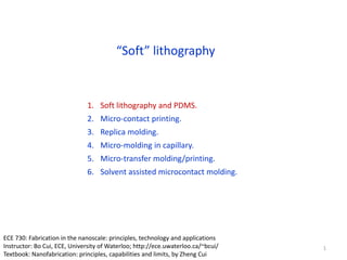
1. “Soft” lithography
1. Soft lithography and PDMS.
2. Micro-contact printing.
3. Replica molding.
4. Micro-molding in capillary.
5. Micro-transfer molding/printing.
6. Solvent assisted microcontact molding.
1
ECE 730: Fabrication in the nanoscale: principles, technology and applications
Instructor: Bo Cui, ECE, University of Waterloo; http://ece.uwaterloo.ca/~bcui/
Textbook: Nanofabrication: principles, capabilities and limits, by Zheng Cui
2. Soft lithography
George M. Whitesides (Harvard)
Soft lithography:
• Low cost
• Molding, printing or transferring
• Resolution usually not very high
• Application in microfluidic, biomedical …
“Soft” means no energetic
particles (electron, ions) or
radiation (UVs, X-ray) is
involved. Instead, soft
elastomeric stamp is used.
Soft lithography opportunity assessment
“Size is not the only thing that matters, function is more important” (something like this), Whiteside 2
3. PDMS: poly(dimethyl-siloxane)
PDMS properties:
• Silicone elastomer with a range of viscosities
• Flexible (1 MPa Young’s modulus, typical polymer 1 GPa) and easy to mold.
• Elastomer, conforms to surface over large areas.
• Chemically inert, optically transparent
• Low surface energy: bonds reversibly (or permanent).
• Seals to flat and clean surfaces for micro-fluidic channels
• Durable (reusable), low thermal expansion
• Biocompatible (even used for food additive)
• Environmentally safe
• Best Resolution: 2-10 nm (for hard PMDS)
Dow Corning brand
3
4. PDMS surface treatment
Plasma oxidation
Air (10 min)
Upon treatment in oxygen plasma, PDMS seals
to itself, glass, silicon, silicon nitride, and some
plastic materials.
contact PDMS surfaces
Irreversible seal:
formation of covalent bonds
Biggest issue: it becomes hydrophobic quickly, very bad for micro-fluidic applications.
(liquid hard to get into the channels once it becomes hydrophobic)
PMDS is absolutely the most popular material for bio-medical lab-on-chip (microfluidic) applications,
but may not be suitable for commercial applications, which need chemically stable surface.
4
5. PDMS problems: soft, low Young’s modulus
Shrinking makes accurate (< few
m) alignment very difficult.
5
8. Test structures in Au, smallest dimension 400nm
Micro - contact printing (μCP)
8
9. Micro - contact printing (μCP), with roller
Xia & Whitesides, Angew. Chem. Int. Ed. 1998, 37, 550-575.
A. Kumar & G. Whitesides, Applied Physics Lett. 1993
a. Printing on a planar surface with a
planar stamp.
b. Printing on a planar surface with a
rolling stamp
c. Printing on a non-planar surface
with a planar stamp
9
12. Replica molding (REM)
Xia & Whitesides et al, Advanced Materials, 1997, 9, 147
PU = polyurethane
It is similar to UV-curing nanoimprint lithography
12
16. Uses capillary forces to fill the gaps between substrate and PDMS master.
1. The PDMS master is pressed tightly on a planar substrate.
2. Elastic PDMS seals off walls and creates capillary channels.
3. A drop of liquid prepolymer is placed at the ends of these channels and
fills them automatically due to capillary force.
4. PDMS can absorb the solvent, which creates a partial vacuum inside the
PDMS cavity and helps to draw in liquid polymer.
5. Cure and peel of the PDMS master.
Micro-molding in capillary (MIMIC)
Line-width: 100nm
Liquid pre-
polymer
Nano-molding in
capillaries is possible 16
17. Micro-molding in capillary (MIMIC)
Kim & Whitesides et al, Nature, 1995, 376, 581
Xia, Y.; Whitesides, G. M. Ann. Rev. Mater. Sci 1998, 28, 153.
a: PU (polyurethane) on Si b: polyaniline c: ZrO2
d: polystryene colloids e+f: free standing PU
17
19. • Apply the liquid prepolymer
• Planarize the prepolymer
• Place the master on a planar substrate
• UV exposure or heating solidifies the
prepolymer that sticks to the substrate
Micro - transfer molding (μTM)
TM fabrication of a). one-layer microstructures;
b). three-layer polymer microstructures.
PDMS
Pre-polymer
Substrate
19
20. Micro - transfer molding (μTM)
Zhao & Whitesides et al, Advanced Materials, 1996, 8, 837.
Microstructures fabricated using TM.
a) An SEM image of a fractured sample showing a
pattern of isolated stars of UV-cured polyurethane
(NOA 73) on Ag.
b) An array of parallel lines of spin-on glass on Si with an
aspect ratio (height/width) of 8.
c) A two-layer structure: isolated micro-cylinders (1.5m
in diameter) on 5m-wide lines, supported on a glass
cover slide.
d) A two-layer structure: a continuous web over a layer
of 5m-wide lines, supported on a glass cover slide.
e) A three-layer structure on a glass cover slide. The
layers of 4 m-wide lines are oriented at 60o from
each other.
Structures in c-e were made of heat-cured epoxy
(F109CLR).
20
21. Metal transfer assisted nanolithography
a) SEM image of the transferred metal grating onto
PMMA layer with period of 700nm on SiO2 substrate.
b) Period 220nm on PET substrate.
c) After O2 RIE of b.
d) After metallization and lift-off process of c.
Guo, “Metal transfer assisted nanolithography on rigid and flexible substrates”, JVST B, 2008
21
Glass transition temperature is 105oC
22. Metal transfer assisted nanolithography: line-width reduction
Schematic of shadow (angle) evaporation of metals to
reduce pattern line-width. The line-width is reduced by
the thickness of the metal on the PDMS grating sidewall.
SEM image of the metal grating on PET substrate after
line-width reduction. The inset is a zoom-in view
showing that the line-width was reduced to 50nm.
22
24. Solvent assisted microcontact molding (SAMIM)
(solvent assisted imprinting)
Kim & Whitesides et al, Advanced Materials, 1997, 9,651.
Substrates
Silicon
Glass
Flexible transparency
Polymer
SU-8 (1μm)
Shipley 1805 Photoresist (500nm)
3% PMMA (70nm)
Solvent
SU-8 (ethanol)
Shipley 1805 photoresist (ethanol)
3% PMMA (acetone)
Uses a solvent to wet the PDMS stamp and soften the structure polymer.
Dissipate and evaporate the solvent through PDMS.
(PDMS stamp can absorb the solvent because of the solvent permeability of PDMS.)
The molded polymer structure becomes solidified in a
few minutes after evaporation of solvent, while the
stamp is still in conformable contact with the substrate.
24
26. SAMIM of PMMA in acetone
Au structure fabrication
26
27. Advantages:
• Convenient and low cost
• Rapid prototyping
• Deformation of PDMS provides route to
complex patterns
• No optical diffraction limit
• Non-planar or curved surfaces
• Generation of 3D -structures
• Control over surface chemistry
• A broad range of materials
• Applicable to manufacturing
• Patterning over large areas
Disadvantages:
• Distortion of patterns
• Poor registration/alignment
• Compatibility with IC processes
• Defects and their densities
• μCP can only be applied to a
number of surfaces
• MIMIC is a relatively slow process
Soft lithography: advantages and disadvantages
27
34. Low temperature co-fired ceramic
processing
• The very rapid evolution of semiconductor IC technology has put immense
pressure on the packaging technologies.
• The new packages must have increasingly smaller footprints, simultaneously
offering improved performance in handling high frequency clocks, very large
number of pin-outs and capability to handle and dissipate large heat densities.
• In other realms there is a need for multilayer solution for miniaturizing the HF
circuits in GHz range, while the Micro Electro Mechanical System (MEMS)
devices need an one technology solution for packaging sensors / actuators
requiring electrical, optical, fluidic and mechanical ‘interconnects’.
• The Low Temperature Co-fired Ceramic (LTCC) Technology offers and
‘integrated’ solutions to these problems.
35. LTCC (Low Temperature Co-fired Ceramics) is a multi-layer glass ceramic
substrate which is Co-fired with low resistance metal conductors at low firing
temperature (less than 1000℃). It is sometimes referred to as "Glass Ceramics"
because its composition consists of glass and alumina.
38. LTCC Fabrication Process
• The process starts with via punching of each layer as per individual layer design.
• If the layer requires any open or buried cavity, it is prepared using the same machine.
• The alignment holes are also punched using via puncher.
• Via filling is done subsequently, using stencil printing.
• This is followed by screen printing of conductor pattern using usual screen printing process.
• Once individual layers are ready, those layers are stacked in sequence, and aligned
mechanically.
• The stacks are then sealed in a plastic bag are and laminated under prescribed temperature-
pressure cycle using isostatic laminator.
• The individual circuits are then singulated using cutter and fired using a special programmable
batch furnace.
• All the fabrication processes described above, are carried out in Class 10000 Clean Room.
• For preparing packages, there are two main post firing processes that remain at this stage. One,
processes for preparing BGA, and second, processes for sealing. We have chosen two possible
options for sealing processes, viz. Solder sealing and Seam sealing and three BGA
formation processes, viz. sphere attachment, stencil printing and electroplating. Following
is the brief description of sealing and BGA formation processes.
39. Solder sealing
Solder sealing is done using solder performs. This needs conducting and
solderable surfaces on either side. Further, interconnection from lid to base would
also require similar pads. As per present plan, these conducting surfaces would
be made using a co-fired Ag-Pd paste. Finally, solder sealing is done by reflow
after components are placed.
Seam Sealing
Seam sealing requires brazing of metallic parts to the ceramic substrate. Brazing
is a three step process that requires post-fire adhesion layer, post fire barrier layer,
brazing layer, each being individually printed and fired. The brazing layer is a low
temperature alloy, and is required to be fired with the metallic part. The BGA could
then be formed by one of the processes described below. It may be noted here
that final sealing process by seam sealing can be done only after components are
placed inside the base.
BGA Formation Processes
The three process options selected here have their own advantages and disadvantages. Sphere
attachment is done using pre-formed solder spheres which could be attached using another
solder paste or through reflow of the same BGA spheres. This process is simple, and cheap, but
has limitations in terms of minimum BGA size. The stencil printing process is also cheap, slightly
more process dependent but can make BGAs with sizes up to even 100µm but with relaxed
pitch. The electroplating process is having more process steps making it costlier, but is capable
of even sub-100µm BGA with equal pitch. Through the present project we are attempting an
exploration of each one of this process. The materials selection for each process has to be done
very carefully so as to ensure subsequently lower temperature steps.
40. Sphere Attachment
BGA by solder sphere attachment is done by directly placing micro-spheres of high-Pb
solder on conducting pads with high alignment accuracy. The solder pads are
dispensed with a viscous flux or attachment solder paste prior to this placement. Reflow
of these solder spheres or attachment solder paste would produce BGAs.
Stencil printing
For good adhesion, one requires Under Bump Metallurgy (UBM) or adhesion
/ barrier layers before solder deposition. High lead Sn-Pb Solder is deposited
by printing solder paste onto the Under Bump Metallurgy (UBM) by stencil
printing process and reflowing the solder paste to form a spherical solder
bump.
Electroplating
In this case the UBM consists typically of an evaporated adhesion layer that provides
conducting path for electroplating, followed by photolithography to open areas of BGA
pads. The BGA pads are then electroplated with adhesion enhancing and solder-barrier
layers. Plating of the high lead Sn-Pb solder alloy is then done over the UBM followed by
removal of resist and underlying evaporated seed layer. The final step is of reflow that
forms the solder bump.
41. LTCC Advantages
•Multilayer capability- means interconnect density limited only by the installed
process capabilities
•Compatibility with flip chip process
means capability to handle and redistribute large number of I/Os
•Capability to integrate passives
means appropriation of additional components within the package which otherwise are
accommodated out of the package
•HF capability up to millimeter wave…
means integration of front-end modules in communication devices
•Integration of Si and other technology devices simultaneously
Flexibility to choose integration scheme
•but the system designer has to work in tandem with chip manufacturers
Ceramic process brings high reliability
•Capability of handling electrical, optical, fluidic and mechanical interconnects in
and out of the package
Amenable to automated wafer assembly; useful tool for fast prototyping
•TCE matching with semiconductor device materials
High working temperature
42. Application examples
- Nozzles that require conductors.
• Nozzle for atmospheric pressure plasma cleaning equipment.
It is possible to appropriately design the internal conductor pattern shape and the
distance between conductors depending on the type of gas used. The shape for
rectification at the nozzle tip is also available.
- Substrate utilizing the hollow as a flow path.
• Sensor unit that analyzes gas and liquid components.
• Substrate that resists high temperatures by the flow of cooling gas and liquid through
it.
- Substrate with special characteristics, created by filling the hollow part with a
different material.
• Substrate with excellent high frequency characteristics.
• Substrate filled with high shielding material to reduce signal interference.
• High heat dissipation substrate filled with high heat dissipation material.
- Built-in integrated component substrate for miniaturization and space saving.
(Note: The mounting part requires an opening)
• Component mounting, or built-in cavity substrate.
- Substrate that requires partial thermal insulation due to product configuration.
• Substrate where the effective temperature range differs between the upper and lower