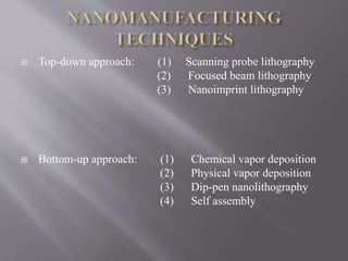
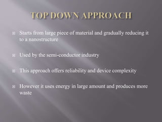
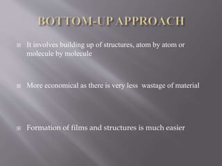
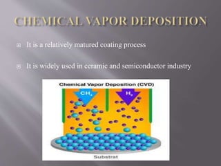
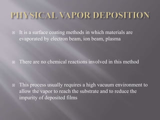
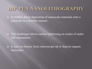
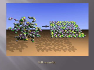
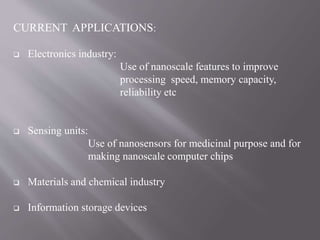
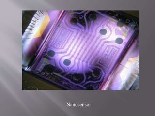
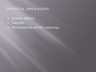
BY
AKSHAY S. MARATHE
CAD-CAM
 The term was first proposed by K. Eric Drexler in the 1970's.
 A nanometer is one billionth of a meter.
 It is the manipulation of matter on an atomic and molecular
scale.
 It is currently undergoing extensive development
Definition:
Nanomanufacturing is both the production of nanoscaled
materials, which can be powders or fluids, and the
manufacturing of parts "bottom up" from nanoscaled
materials or "top down" in smallest steps for high precision
 Materials exhibit unique properties at these scales
 Increase in toughness
 High hardness
 Low thermal co-efficient of expansion
 Top-down approach: (1) Scanning probe lithography
(2) Focused beam lithography
(3) Nanoimprint lithography
 Bottom-up approach: (1) Chemical vapor deposition
(2) Physical vapor deposition
(3) Dip-pen nanolithography
(4) Self assembly
 Starts from large piece of material and gradually reducing it
to a nanostructure
 Used by the semi-conductor industry
 This approach offers reliability and device complexity
 However it uses energy in large amount and produces more
waste
 It is a mechanical approach to realize patterning
 Different configurations are available such as Scanning
tunneling microscope and Atomic force microscope
Mechanical patterning
Scanning tunneling microscope
Block diagram of Atomic force microscope
 It is a high resolution patterning method where electron or
ion beam is used
 Uses modern electron microscope
 High-energy ions tend to damage the sample surface
 It is a method of fabricating nanometer scale patterns
 It creates patterns by mechanical deformation of imprint resist and
subsequent processes
 It is able to replicate sub-10 nm patterns with high throughput
Nano-imprint lithography
 It involves building up of structures, atom by atom or
molecule by molecule
 More economical as there is very less wastage of material
 Formation of films and structures is much easier
 It is a relatively matured coating process
 It is widely used in ceramic and semiconductor industry
 It is a surface coating methods in which materials are
evaporated by electron beam, ion beam, plasma
 There are no chemical reactions involved in this method
 This process usually requires a high vacuum environment to
allow the vapor to reach the substrate and to reduce the
impurity of deposited films
 It enables direct deposition of nanoscale materials onto a
substrate in a flexible manner
 This technique allows surface patterning on scales of under
100 nanometers
 It uses an Atomic force microscope tip to deposit organic
molecules
Molecular ink diffusing from a nanoscale
tip to a surface through a water meniscus
 It is the autonomous organization of components into patterns or
structures without human intervention
 Many biological systems use self-assembly to assemble various
molecules and structures
 Manufacturing will benefit from applications of self-
assembly
CURRENT APPLICATIONS:
 Electronics industry:
Use of nanoscale features to improve
processing speed, memory capacity,
reliability etc
 Sensing units:
Use of nanosensors for medicinal purpose and for
making nanoscale computer chips
 Materials and chemical industry
 Information storage devices
Nanosensor
POTENTIAL APPLICATIONS:
 Aviation industry
 Nano bots
 Pharmaceuticals and Bio- technology
THANK YOU

Nanomanufacturing ppt

  • 1.
  • 2.
     The termwas first proposed by K. Eric Drexler in the 1970's.  A nanometer is one billionth of a meter.  It is the manipulation of matter on an atomic and molecular scale.  It is currently undergoing extensive development
  • 3.
    Definition: Nanomanufacturing is boththe production of nanoscaled materials, which can be powders or fluids, and the manufacturing of parts "bottom up" from nanoscaled materials or "top down" in smallest steps for high precision
  • 4.
     Materials exhibitunique properties at these scales  Increase in toughness  High hardness  Low thermal co-efficient of expansion
  • 5.
     Top-down approach:(1) Scanning probe lithography (2) Focused beam lithography (3) Nanoimprint lithography  Bottom-up approach: (1) Chemical vapor deposition (2) Physical vapor deposition (3) Dip-pen nanolithography (4) Self assembly
  • 6.
     Starts fromlarge piece of material and gradually reducing it to a nanostructure  Used by the semi-conductor industry  This approach offers reliability and device complexity  However it uses energy in large amount and produces more waste
  • 7.
     It isa mechanical approach to realize patterning  Different configurations are available such as Scanning tunneling microscope and Atomic force microscope Mechanical patterning
  • 8.
  • 9.
    Block diagram ofAtomic force microscope
  • 10.
     It isa high resolution patterning method where electron or ion beam is used  Uses modern electron microscope  High-energy ions tend to damage the sample surface
  • 11.
     It isa method of fabricating nanometer scale patterns  It creates patterns by mechanical deformation of imprint resist and subsequent processes  It is able to replicate sub-10 nm patterns with high throughput
  • 12.
  • 13.
     It involvesbuilding up of structures, atom by atom or molecule by molecule  More economical as there is very less wastage of material  Formation of films and structures is much easier
  • 14.
     It isa relatively matured coating process  It is widely used in ceramic and semiconductor industry
  • 15.
     It isa surface coating methods in which materials are evaporated by electron beam, ion beam, plasma  There are no chemical reactions involved in this method  This process usually requires a high vacuum environment to allow the vapor to reach the substrate and to reduce the impurity of deposited films
  • 17.
     It enablesdirect deposition of nanoscale materials onto a substrate in a flexible manner  This technique allows surface patterning on scales of under 100 nanometers  It uses an Atomic force microscope tip to deposit organic molecules
  • 18.
    Molecular ink diffusingfrom a nanoscale tip to a surface through a water meniscus
  • 19.
     It isthe autonomous organization of components into patterns or structures without human intervention  Many biological systems use self-assembly to assemble various molecules and structures  Manufacturing will benefit from applications of self- assembly
  • 21.
    CURRENT APPLICATIONS:  Electronicsindustry: Use of nanoscale features to improve processing speed, memory capacity, reliability etc  Sensing units: Use of nanosensors for medicinal purpose and for making nanoscale computer chips  Materials and chemical industry  Information storage devices
  • 22.
  • 23.
    POTENTIAL APPLICATIONS:  Aviationindustry  Nano bots  Pharmaceuticals and Bio- technology
  • 24.