Downloaded 327 times

![Engineering Physics B.Tech:2012-13
LECTURE NOTE: ENGINEERING PHYSICS, SUBJECT CODE: BSPH1203
[For B.Tech, 1st
Semester CSE, 2nd
Semester ECE, EEE, EE of CENTURION
UNIVERSITY OF TECHNOLOGY AND MANAGEMENT]
Module-1
Session-1
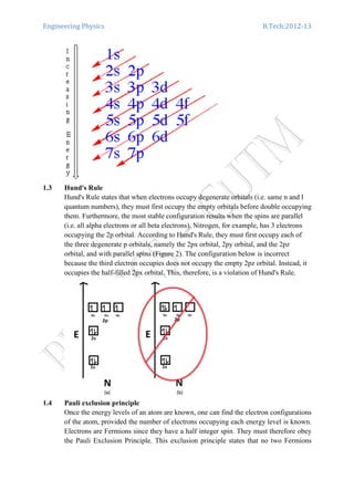
1.1 Introduction: Atomic structure
All matter is formed from basic building blocks called atoms. Atoms are made of
even smaller particles called protons, electrons, and neutrons. Protons and neutrons
live in the nucleus of an atom and are almost identical in mass. However, protons
have positive charges whereas neutrons have no charge. Electrons have a negative
charge and orbit the nucleus in shells or electron orbitals and are much less massive
than the other particles. Since electrons are 1836 times less massive than either
protons or neutrons, most of the mass of an atom is in the nucleus, which is only
1/100,000th the size of an entire atom
1.2 Madelung's Rule:](https://image.slidesharecdn.com/engineeringphysics-151212062959/85/Engineering-physics-2-320.jpg)
![Engineering Physics B.Tech:2012-13
can occupy the same energy level corresponding to a unique set of quantum numbers
n, l, m or s. The ground state of an atom is therefore obtained by filling each energy
level, starting with the lowest energy, up to the maximum number as allowed by the
Pauli Exclusion Principle.
1.5 Electronic configuration of the elements
The electronic configuration of the elements of the periodic table can be constructed
using the quantum numbers of the hydrogen atom and the Pauli exclusion principle,
starting with the lightest element hydrogen. Hydrogen contains only one proton and
one electron. The electron therefore occupies the lowest energy level of the hydrogen
atom, characterized by the principal quantum number n = 1. The orbital quantum
number, l, equals zero and is referred to as an s orbital (not to be confused with the
quantum number for spin, s).The s orbital can accommodate two electrons with
opposite spin, but only one is occupied. This leads to the shorthand notation of 1s1
for
the electronic configuration of hydrogen as listed in Table 1.2.3. This table also lists
the atomic number (which equals the number of electrons), the name and symbol, and
the electronic configuration of the first 36 elements of the periodic table.
Helium is the second element of the periodic table. For this and all other atoms one
still uses the same quantum numbers as for the hydrogen atom. This approach is
justified since all atom cores can be treated as a single charged particle, which yields a
potential very similar to that of a proton. While the electron energies are no longer the
same as for the hydrogen atom, the electron wave functions are very similar and can
be classified in the same way. Since helium contains two electrons it can
accommodate two electrons in the 1s orbital, hence the notation 1s2
. Since the s
orbitals can only accommodate two electrons, this orbital is now completely filled, so
that all other atoms will have more than one filled or partially filled orbital. The two
electrons in the helium atom also fill all available orbitals associated with the first
principal quantum number, yielding a filled outer shell. Atoms with a filled outer shell
are called noble gases, as they are known to be chemically inert.
Lithium contains three electrons and therefore has a completely filled 1s orbital and
one more electron in the next higher 2s orbital. The electronic configuration is
therefore 1s2
2s1
or [He]2s1
, where [He] refers to the electronic configuration of
helium. Beryllium has four electrons, two in the 1s orbital and two in the 2s orbital.
The next six atoms also have a completely filled 1s and 2s orbital as well as the
remaining number of electrons in the 2p orbitals. Neon has six electrons in the 2p
orbitals, thereby completely filling the outer shell of this noble gas.
The next eight elements follow the same pattern leading to argon, the third noble gas.
After that the pattern changes as the underlying 3d orbitals of the transition metals
(scandium through zinc) are filled before the 4p orbitals, leading eventually to the
fourth noble gas, krypton. Exceptions are chromium and zinc, which have one more](https://image.slidesharecdn.com/engineeringphysics-151212062959/85/Engineering-physics-4-320.jpg)

![Engineering Physics B.Tech:2012-13
Session-2
2.1. Electrical Conduction: Electrical conductivity of a material is defined in terms of
ease with which a material transmits an electrical current. Electrical current (I) is
flow of electrons, and driving force for the flow of electrons is called voltage (V).
Ohm’s law relates these parameters as follows
V α I
V = IR……………………………….……….[1.1]
where R – is the materials resistance to flow of electrons through it.
V, I, and R respectively have units as volts, amperes, and ohms ( ).
2.2. Electrical Resistivity: Electrical resistance of a material is influenced by its
geometric configuration; hence a new parameter called electrical resistivity (ρ) is
defined such as it is independent of the geometry.
ߩ ൌ
ோ
……………………………..……….[1.2]
where A – cross-sectional area perpendicular to the direction of the current, and l –
the distance between points between which the voltage is applied. Units for ρ are
ohm-meters ( -m).
2.3. Electrical Conductivity: Reciprocal of the electrical resistivity, known as electrical
conductivity (σ), is used to express the electrical behavior of a material, which is
indicative of the ease with which a material allows of flow of electrons.
ߪ ൌ
ଵ
ఘ
ൌ
ோ
…………………………..……..[1.3]
Electrical conductivity has the following units: ( -m)-1
or mho/meter. The
conductivity of material depends on the presence of free electrons or conduction
electrons, which move freely in the metal and do not correspond to any atom. These
electrons are known as electron gas.
2.4. Classification of Conducting Materials: Based on electrical conductivity, materials
can be classified into three categories:
i. Zero resistivity materials
ii. Low resistivity materials
iii. High resistivity materials
(i) Zero resistivity materials: Superconductor like alloys of aluminium, zinc,
gallium, nichrome, niobium, etc. are a special class of materials that conduct
electricity almost with zero resistance below the transition temperature. These
materials are perfect diamagnetic. Such materials are used for energy saving in
power systems, superconducting magnets, memory storage elements.
(ii) Low resistivity materials: The metals and alloys like silver, aluminium have
very high electrical conductivity, in the order of 10଼
Ωିଵ
݉ିଵ
. They are used
as resistors. Conductors, electrical contacts, etc. in electrical devices and also
in electrical power transmission and distribution, winding wires in motors and
transformers.](https://image.slidesharecdn.com/engineeringphysics-151212062959/85/Engineering-physics-6-320.jpg)
![Engineering Physics B.Tech:2012-13
(iii) High resistivity materials: The material like tungsten, platinum, nichrome, etc.
have high resistivity and low temperature coefficient of resistances. Such
metals and alloys are used in the manufacturing of resistors, heating elements,
resistance thermometers, etc.
2.5. Basic Terminologies
1. Bound Electrons:
All the valence electrons in an isolated atom are bound to their
parent nuclei are called as bound electrons.
2. Free electrons:
Electrons which moves freely or randomly in all directions in the
absence of external field.
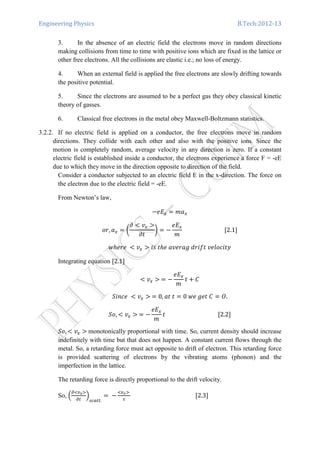
3. Drift Velocity
If no electric field is applied on a conductor, the free electrons
move in random directions. They collide with each other and also with the
positive ions. Since the motion is completely random, average velocity in any
direction is zero. If a constant electric field is established inside a conductor,
the electrons experience a force F = -eE due to which they move in the
direction opposite to direction of the field. These electrons undergo frequent
collisions with positive ions. In each such collision, direction of motion of
electrons undergoes random changes. As a result, in addition to the random
motion, the electrons are subjected to a very slow directional motion. This
motion is called drift and the average velocity of this motion is called drift
velocity vd.
4. Electric Field (E):
The electric field E of a conductor having uniform cross
section is defined as the potential drop (V) per unit length (l).
i.e., E = V/ l V/m
5. Current density (J):
It is defined as the current per unit area of cross section of an
imaginary plane hold normal to the direction of the flow of current in a current
carrying conductor.
J = I/ A Am-2
6. Fermi level
Fermi level is the highest filled energy level at 0 K.
7. Fermi energy
Energy corresponding to Fermi level is known as Fermi energy.
[Reference: Material Science by V. Rajendran and A. Marikani, Pages-7.1-7.2]](https://image.slidesharecdn.com/engineeringphysics-151212062959/85/Engineering-physics-7-320.jpg)
![Engineering Physics B.Tech:2012-13
A
L
d
I
The proportionality constant
ଵ
ఛ
has the unit of sec-1
. So, ߬ is called relaxation time.
In steady state, ቀ
డழ௩ೣவ
డ௧
ቁ
ௗ
ൌ െ ቀ
డழ௩ೣவ
డ௧
ቁ
௦௧௧.
Using eq[2.1] and [2.3], we have
െ
݁ܧ௫
݉
ൌ
൏ ݒ௫
߬
,ݎ ൏ ݒ௫ ൌ െ
݁߬
݉
ܧ௫ ሾ2.4ሿ
We know that, Current density ݆௫ ൌ െ݊݁ ൏ ݒ௫ ሾ2.5ሿ
Where n is the concentration of electrons in the metal.
From eq[2.4] and [2.5],
݆௫ ൌ
݊݁ଶ
߬
݉
ܧ௫ ሾ2.6ሿ
3.2.3 Ohm’s law in terms of E and J
From Ohm’s law ܸ ൌ ܴܫ
V=Potential across the conductor,
I= Current through the conductor
R=Resistance
ߪ=conductivity of the conductor
Let L=length
d=width of conductor
A=area of cross section
Now ܸ ൌ ܧ௫ܮ
ܫ௫ ൌ ܬ௫ܣ
And ܴ ൌ
ఙ
So, Ohm’s law can be written as ܧ௫ܮ ൌ ܬ௫ܣ ൈ
ఙ
Or, ܬ௫ ൌ ߪܧ௫ ሾ2.7ሿ
Equation [2.7] is the ohm’s law
3.2.4 Electrical Conductivity: Comparing eqs[2.6] and [2.7], we get
࣌ ൌ
మఛ
ሾ2.8ሿ
The electrical conductivity is directly proportional to the concentration of free
electrons and the relaxation time.
3.2.5 Electrical Resistivity: ࣋ ൌ
࣌
ൌ
మఛ
[2.9]
3.2.6 Mobility: It is defined as the average drift velocity per unit applied electric field.
So,](https://image.slidesharecdn.com/engineeringphysics-151212062959/85/Engineering-physics-10-320.jpg)
![Engineering Physics B.Tech:2012-13
ߤ ൌ
ݒ
ܧ
ൌ
݁߬
݉
െ ሾ2.10ሿ
Hence
ߪ ൌ ݊݁ߤ. ሾ2.11ሿ
[Reference: Material Science by M. S. Vijaya and G. Rangarajan, Page-203-206]
Session-4
4.1 Interpretation of Relaxation time
From eq[2.3], ቀ
డழ௩ೣவ
డ௧
ቁ
௦௧௧.
ൌ െ
ழ௩ೣவ
ఛ
Let the electric field is switched off at t=0, then the drift velocity gradually falls to
zero, due to scattering by phonons. Integrating above equation
න
߲ ൏ ݒ௫
൏ ݒ௫
ൌ െ න
߲ݐ
߬
Or, ݈݊ ൏ ݒ௫ ൌ െ
௧
ఛ
ܥ [3.1]
At t=0, ൏ ݒ௫ ൌ൏ ݒ௫ሺ0ሻ , so, from eq[3.1], ܥ ൌ ݈݊ ൏ ݒ௫ሺ0ሻ
Putting the value of C, we get
݈݊
൏ ݒ௫
൏ ݒ௫ሺ0ሻ
ൌ െ
ݐ
߬
,ݎ ൏ ݒ௫ ൌ൏ ݒ௫ሺ0ሻ ݁ି
௧
ఛ ሾ3.2ሿ
eq[3.2]shows that, when electric field is switched off, the drift velocity falls
exponentially to zero. The relaxation time is determined by the electron phonon
interaction in the metal. It is of the order of 10-14
sec.
4.2 Temperature Dependence of Electrical Resistivity:
From Kinetic theory, the kinetic energy associated with an electron is
1
2
݉ሺܿ̅ሻଶ
ൌ
3
2
݇ܶ
When an electric field is applied, the resulting acceleration ܽ ൌ
ா
. If the mean free
path is ߣ, then the time between collision is
ఒ
̅
. Hench the drift velocity acquired
before next collision is
ݑ ൌ ݈ܽܿܿ.ൈ ݁݉݅ݐ ൌ ൬
݁ܧ
݉
൰ ൬
ߣ
ܿ̅
൰
Thus the average drift velocity is](https://image.slidesharecdn.com/engineeringphysics-151212062959/85/Engineering-physics-11-320.jpg)
![Engineering Physics B.Tech:2012-13
ݑ
2
ൌ
݁ܧ
2݉
ߣ
ܿ̅
If n is the number of electrons per unit volume, then current density is
ܬ௫ ൌ
݊݁ݑ
2
ൌ
݊݁ଶ
ܧ
2݉
ߣ
ܿ̅
Or
ߪ ൌ
ܬ௫
ܧ
ൌ
݊݁ଶ
2݉
ߣ
ܿ̅
Or,
ߩ ൌ
2݉
݊ߣ݁ଶ
ൈ ඨ
3݇ܶ
݉
ൌ
ඥ12݉݇ܶ
݊݁ଶߣ
െ െ െ െ െ െ െ ሾ3.3ሿ
Here it is assumed that ߣ is independent of temperature. Hence ߩ ∝ √ܶ which is
contradictory to the experimental fact that ߩ ∝ ܶ.
4.3 Drawbacks of Classical free electron theory
1) According to this theory, ߩ is proportional to √ܶ. But experimentally it was found
that ߩ is proportional to T.
2) According to this theory, K/ ߪܶ= L, a constant (Wiedmann-Franz law) for all
temperatures. But this is not true at low temperatures.
3) The theoretically predicted value of specific heat of a metal does not agree with the
experimentally obtained value.
4) This theory fails to explain ferromagnetism, superconductivity, photoelectric effect,
Compton effect and blackbody radiation.
[Reference: Material Science by M. S. Vijaya and G. Rangarajan, Page-206-208]
Session-5
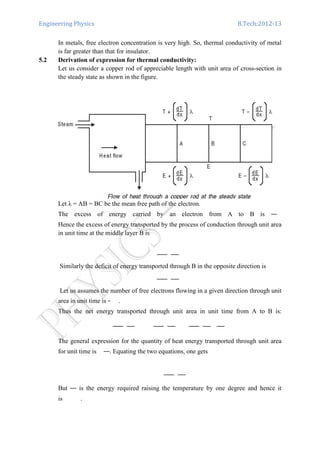
5.1 Thermal conductivity: The thermal conductivity is defined as the ratio of the
amount of heat energy conducted per unit area of cross section per second to the
temperature gradient.
Therefore, the thermal conductivity
ܭ ൌ െ
ܳ
݀ܶ
݀ݔൗ
ሾ4.1ሿ
Where K is the coefficient of thermal conductivity, Q the amount of heat energy
conducted per unit area of cross section in one second and ݀ܶ
݀ݔൗ the temperature
gradient. The negative sign shows that heat flows from the hot end to cold end.
The thermal conductivity of a material, in general, is due to the presence of lattice
vibrations and electrons. Hence, the thermal conduction can be written as
ܭ௧௧ ൌ ܭ௧ ܭ௦
݁ݎ݄݁ݓ ݏ݄݊݊ ܽ݁ݎ ݄݁ݐ ݁݊݁ݕ݃ݎ ܿܽݏݎ݁݅ݎݎ ݂ݎ ݈ܽ݁ܿ݅ݐݐ ݏ݊݅ݐܽݎܾ݅ݒ](https://image.slidesharecdn.com/engineeringphysics-151212062959/85/Engineering-physics-12-320.jpg)
![Engineering Physics B.Tech:2012-13
Now
݇ ൌ
݊ܿ̅ߣ
3
ሺܥ௩ሻ ൌ
݊ߣ
3
ሺܥ௩ሻඨ
3݇ܶ
݉
But ሺܥ௩ሻ ൌ
ଷ
ଶ
݇ with n=1 electron
Thus,
݇ ൌ
݊ߣ
3
൬
3
2
݇൰ ඨ
3݇ܶ
݉
ൌ
݊ߣ݇
2
ඨ
3݇ܶ
݉
ሾ4.2ሿ
5.3 Wiedmann-Franz law:
This law states that when the temperature is not too law, the ratio of the thermal
conductivity to the electrical conductivity of a metal is directly proportional to the
absolute temperature, i.e.,
ఙ
∝ ܶ
Or,
ܭ
ߪܶ
ൌ ܿݐ݊ܽݐݏ݊ ൌ ܮ ሾ4.3ሿ
Where L is a constant known as Lorentz number.
From the expression for the thermal conductivity and electrical conductivity, the ratio
can be written as,
ܭ
ߪ
ൌ
݊ߣ݇
2
ට3݇ܶ
݉
ൈ
ඥ12݉݇ܶ
݊݁ଶߣ
ൌ 3 ൬
݇
݁
൰
ଶ
ܶ ሾ4.4ሿ
Or,
ఙ்
ൌ 3 ቀ
ಳ
ቁ
ଶ
which is the Lorentz number.
[Reference: Material Science by V. Rajendran and A. Marikani, Pages-7.5-7.8]
Session-6
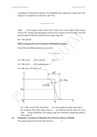
6.1 Quantum free electron theory
Classical free electron theory could not explain many physical properties. In 1928,
Sommerfeld developed a new theory applying quantum mechanical concepts and
Fermi-Dirac statistics to the free electrons in the metal. This theory is called quantum
free electron theory.
Classical free electron theory permits all electrons to gain energy. But quantum free
electron theory permits only a fraction of electrons to gain energy. In order to
determine the actual number of electrons in a given energy range (dE), it is necessary
to know the number of states (dNs) which have energy in that range. The number of
states per unit energy range is called the density of states g(E).
Therefore, g(E) = dNs/dE](https://image.slidesharecdn.com/engineeringphysics-151212062959/85/Engineering-physics-14-320.jpg)
![Engineering Physics B.Tech:2012-13
And conductivity ࣌ ൌ
మఛ
where ߬ is the average time elapsed after collision.
The real picture of electrical conduction in metal is quite different from the classical
one, in which it was assumed that the current carried equally by all electrons, each
moving with an average drift velocity ݒௗ. But quantum mechanical treatment tells us
that the current is in fact, carried out by very few electrons only, all moving at high
velocity (ݒி).
If λ is the mean free paths and ݒி is the speed of free electrons whose kinetic energy
is equal to Fermi energy since only electrons near Fermi level contributes to the
conductivity. The average time τ between collisions is given by ߬ ൌ
ఒ
ಷ
Thus the electric conductivity
࣌ ൌ
మఒ
ಷ
ሾ5.2ሿ
The only quantity which depends on temperature is the mean free path. Since this free
path is inversely proportional to temperature at high temperature. It follows that,
ߪ ∝
ଵ
்
ߩ ݎ ∝ ܶ, in agreement with experimental conclusion.
it is obvious at a given temperature the only factor which varies from one metal to the
other is densities of free electron. One must also note that the energy kT (where T is
of the order of 300 k) can activate only the free electrons near the Fermi level to move
to unoccupied states and contribute to specific heat. We may therefore require an
energy EF called (very high compared with kT = 0.025 eV at 300 k) Fermi energy to
make all the electrons to move to the unoccupied states corresponding to a
temperature TF called Fermi temperature. The unique relation connecting the various
parameters in quantum theory of free electron is
ܧி ൌ
1
2
ܸ݉ி
ଶ
ൌ ݇ܶி
[Reference: Material Science by M. S. Vijaya and G. Rangarajan, Page-212-226]
Session-7
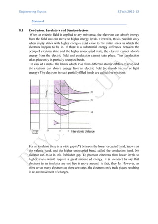
7.1 Band theory of solids
The atoms in the solid are very closely packed. The nucleus of an atom is so heavy
that it considered being at rest and hence the characteristic of an atom are decided by
the electrons. The electrons in an isolated atom have different and discrete amounts of
energy according to their occupations in different shells and sub shells. These energy
values are represented by sharp lines in an energy level diagram.
During the formation of a solid, energy levels of outer shell electrons got split up. As
a result, closely packed energy levels are produced. The collection of such a large
number of energy levels is called energy band. The electrons in the outermost shell
are called valence electrons. The band formed by a series of energy levels containing
the valence electrons is known as valence band. The next higher permitted band in a](https://image.slidesharecdn.com/engineeringphysics-151212062959/85/Engineering-physics-16-320.jpg)
![Engineering Physics B.Tech:2012-13
solid is the conduction band. The electrons occupying this band are known as
conduction electrons.
Conduction band valence band are separated by a gap known as forbidden energy gap.
No electrons can occupy energy levels in this band. When an electrons in the valence
band absorbs enough energy, it jumps across the forbidden energy gap and enters the
conduction band, creating a positively charged hole in the valence band. the hole is
basically the deficiency of an electron.
7.2 Energy Band Diagram
Electrical properties of materials are best understood in terms of their electronic
structure. We know that the energy levels of isolated atoms are discrete. When atoms
are brought together to form a solid, these energy levels spread out into bands of
allowed energies. The effect is qualitatively understood as follows by considering
what happens when a collection of atoms, which are initially far apart are brought
closer.
When the spacing between adjacent atoms is large, each atom has sharply defined
energy levels which are denoted by etc. As the atoms are far apart their orbitals do not
overlap. In particular if each atom is in its ground state, the electrons in each atom
occupy identical quantum states. As the distance starts decreasing, the orbitals
overlap. The electrons of different atoms cannot remain in the same state because of
Pauli Exclusion Principle. Pauli principle states that a particular state can at most
accommodate two electrons of opposite spins. Thus when atoms are brought together,
the levels must split to accommodate electrons in different states. Though they appear
continuous, a band is actually a very large number of closely spaced discrete levels
[Reference: Material Science by V. Rajendran and A. Marikani, Pages-8.22-8.23]
[Reference: Material Science by M. S. Vijaya and G. Rangarajan, Page-226-229]](https://image.slidesharecdn.com/engineeringphysics-151212062959/85/Engineering-physics-17-320.jpg)
![Engineering Physics B.Tech:2012-13
Semiconductors, like insulator have band gaps. However, the gap between the top of
the valence band and the bottom of the conduction band is much narrower than in an
insulator. For comparison, the gap in case of Silicon is 1.1 eV while that for diamond,
which is an insulator, is about 6 eV.
[Reference: Material Science by M. S. Vijaya and G. Rangarajan, Page-230-232]
[Reference: Material Science by V. Rajendran and A. Marikani, Pages-8.23-8.24 &
9.1-9.2]
Session-9
9.1 Semiconductors
Elemental are semiconductors where each atom is of the same type such as Ge, Si.
These atoms are bound together by covalent bonds, so that each atom shares an
electron with its nearest neighbour, forming strong bonds. Compound semiconductors
are made of two or more elements. Common examples are GaAs or InP. These
compound semiconductors belong to the III-V semiconductors so called because first
and second elements can be found in group III and group V of the periodic table
respectively. In compound semiconductors, the difference in electro-negativity leads
to a combination of covalent and ionic bonding. Ternary semiconductors are formed
by the addition of a small quantity of a third element to the mixture, for example Al x
Ga 1-x As. The subscript x refers to the alloy content of the material, what proportion
of the material is added and what proportion is replaced by the alloy material. The
addition of alloys to semiconductors can be extended to include quaternary materials
such as Ga x In (1-x) As y P (1-y) or GaInNAs and even quinternary materials such as
GaInNAsSb. Once again, the subscripts denote the proportion elements that constitute
the mixture of elements. Alloying semiconductors in this way allows the energy gap
and lattice spacing of the crystal to be chosen to suit the application.
Valence band
Very large energy gap
Conduction
band empty
Valence band
Large energy gap
Conduction band
Valence band
Small energy gap
Conduction band
Figure 2
Insulators
Semiconductors
Conductors](https://image.slidesharecdn.com/engineeringphysics-151212062959/85/Engineering-physics-19-320.jpg)
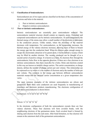
![Engineering Physics B.Tech:2012-13
this whole process the no of holes and the free electrons in the circuit of the intrinsic
semi conductor will be same.
[Reference: Material Science by V. Rajendran and A. Marikani, Pages-9.2-9.5]
[Reference: Material Science by M. S. Vijaya and G. Rangarajan, Page-263]
Session-10
10.1 Doped or extrinsic semiconductors:
Those semiconductors in which some impurity atoms are embedded are known as
extrinsic semiconductors. The process of adding impurity to the intrinsic
semiconductor is known as doping.
Extrinsic semi conductors are basically of two types:
1. P-type semi conductors
2. N-type semi conductors
10.2 N-type Semi conductors: Let’s take an example of the silicon crystal to understand
the concept of N-type semi conductor. We have studied the electronic configuration
of the silicon atom. It has four electrons in its outermost shell. In N-type semi
conductors, the silicon atoms are replaced with the pentavalent atoms like
phosphorous, bismuth, antimony etc. So, as a result the four of the electrons of the
pentavalent atoms will form the covalent bonds with the silicon atoms and the one
electron will revolve around the nucleus of the impurity atoms with less binding
energy. These electrons are almost free to move. In other words we can say that these
electrons are donated by the impure atoms. So, these are also known as donor atoms.
So, the conduction inside the conductor will take place with the help of the negatively
charged electrons. Electrons are negatively charged. Due to this negative charge these
semiconductors are known as N-type semiconductors.
Each donor atom has denoted an electron from its valence shell. So, as a result due to
loss of the negative charge these atoms will become positively charged. The single
valence electron revolves around the nucleus of the impure atom. The extra valance
electron not needed for the sp3
tetrahedral bonding is only loosely bound to the P
atom in a donor energy level, Ed. The energy of this donor energy level is close to the
lowest energy level of the conduction band (in Si it is 0.4 eV) and so it is easy to
promote an electron from the donor level to the conduction band. These promoted
electrons become charge carriers that contribute to the material's conductivity. Since
they are negative, the result is called an n-type semiconductor.
When the semi conductors are placed at room temperature then the covalent bond
breakage will take place. So, more free electrons will be generated. As a result, same](https://image.slidesharecdn.com/engineeringphysics-151212062959/85/Engineering-physics-22-320.jpg)
![Engineering Physics B.Tech:2012-13
no of holes generation will take place. But as compared to the free electrons the no of
holes are comparatively less due to the presence of donor electrons.
We can say that major conduction of n-type semi conductors is due to electrons. So,
electrons are known as majority carriers and the holes are known as the minority
carriers.
[Reference: Material Science by M. S. Vijaya and G. Rangarajan, Page-264]
[Reference: Material Science by V. Rajendran and A. Marikani, Pages-9.5-9.6]
Session-11
11.1 P-type semi conductors: In a p-type semi conductor doping is done with trivalent
atoms. Trivalent atoms are those which have three valence electrons in their valence
shell. Some examples of trivalent atoms are Aluminium, boron etc. So, the three
valence electrons of the doped impure atoms will form the covalent bonds between
silicon atoms. But silicon atoms have four electrons in its valence shell. So, one
covalent bond will be improper. So, one more electron is needed for the proper
covalent bonding. This need of one electron is fulfilled from any of the bond between
two silicon atoms. So, the bond between the silicon and indium atom will be
completed. After bond formation the indium will get ionized. As we know that ions
are negatively charged. So, indium will also get negative charge. A hole was created
when the electron come from silicon-silicon bond to complete the bond between
indium and silicon. Now, an electron will move from any one of the covalent bond to
fill the empty hole. This will result in a new holes formation. So, in p-type semi
conductor the holes movement results in the formation of the current. Holes are
positively charged. Hence these conductors are known as p-type semiconductors or
acceptor type semi conductors.
P-type semiconductors have dopants from the IIIA group such as B+3
. These donor
impurity atoms in substitutional solid solution. The lack of an electron needed for sp3
tetrahedral bonding is easily filled by a neighbouring Si atom into an acceptor energy](https://image.slidesharecdn.com/engineeringphysics-151212062959/85/Engineering-physics-23-320.jpg)
![Engineering Physics B.Tech:2012-13
level, Ea of the dopant atom. The energy of this acceptor level is only slightly above
the valance band and so it is easy to promote an electron from the valance band into it.
For each promotion of an electron into one of these acceptor levels, a hole is left in
the valance band. It is these holes that become the charge carriers and contribute to
the conductivity of the semiconductor. Since these holes are positive, the result is
called a p-type semiconductor.
Note that the temperatures needed to promote the dopant electrons into the conduction
band are lower than the temperatures required to promote the intrinsic electrons into
the conduction band.
When these conductors are placed at room temperature then the covalent bond
breakage will take place. In this type of semi conductors the electrons are very less as
compared to the holes. So, in p-type semi conductors holes are the majority carriers
and electrons are the minority carriers.
[Reference: Material Science by M. S. Vijaya and G. Rangarajan, Page-264-265]
[Reference: Material Science by V. Rajendran and A. Marikani, Pages-9.6]
Session-12
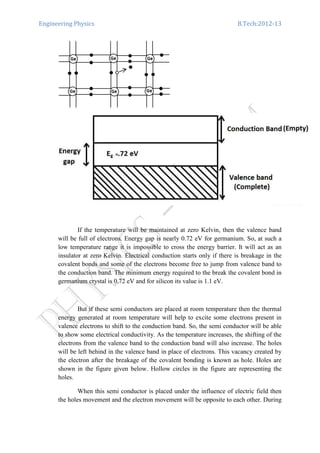
12.1 Hall effect:
Consider a rectangular slab that carries a current I in the X-direction. A uniform
magnetic field of flux density B is applied along the Z-direction. The current carriers
experience a force (Lorentz force) in the downward direction. This leads to an
accumulation of electrons in the lower face of the slab. This makes the lower face
negative. Similarly the deficiency of electrons makes the upper face positive. As a
result, an electric field is developed along Y-axis. This effect is called Hall effect and
the emf thus developed is called Hall voltage VH. The electric field developed is
called Hall field EH.](https://image.slidesharecdn.com/engineeringphysics-151212062959/85/Engineering-physics-24-320.jpg)
![Engineering Physics B.Tech:2012-13
ܴு ൌ
ܧு
݆௫ܤ
ሾ12.3ሿ
i.e.,
ܴு ൌ
1
݊݁
ሾ12.4ሿ
In this case
ܴு ൌ െ
1
݊݁
ሾ12.5ሿ
Negative sign is used because the electric field developed is in the negative y-
direction.
ܴு ൌ െ
ܧு
݆௫ܤ
ൌ െ
1
݊݁
ሾ12.6ሿ
All the three quantities ܧு, B and ݆௫ cab be measured, and so the Hall coefficient and
carrier density can be found out.
For a p-type specimen, the current is due to holes. In this case
ܴு ൌ
ܧு
݆௫ܤ
ൌ
1
݁
ሾ12.7ሿ
Where p is positive hole density.
12.2 Determination of the Hall coefficient
The Hall coefficient is determined by measuring the Hall voltage that generates the
Hall field. If VH is the Hall Voltage across the sample of width d, then
ܸு ൌ ܧு݀
Substituting for ܧு from equation [10.3], we get
ܸு ൌ ܴ݀ܤு݆௫ ሾ12.8ሿ
If t is the thickness along the magnetic field of sample, then its cross section will be dt
and the current density ݆௫ ൌ
ܫ௫
݀ݐ
ൗ , thus
ܸு ൌ
ܴுܫ௫݀ܤ
݀ݐ
ൌ
ܴுܫ௫ܤ
ݐ
Hence,
ܴு ൌ
ܸுݐ
ܫ௫ܤ
ሾ12.9ሿ
The polarity of ܸு will be opposite for n- and p-type semiconductor.
[Reference: Material Science by V. Rajendran and A. Marikani, Pages-10.13-10.17]
[Reference: Material Science by M. S. Vijaya and G. Rangarajan, Page-274-275]
Session-13
13.1 Superconductivity: (DoITPoMS - TLP Library Superconductivity)
INTRODUCTION: The phenomenon of superconductivity was first discovered by
Kammerlingh Onnes in 1911. He found that electrical resistivity of some metals,](https://image.slidesharecdn.com/engineeringphysics-151212062959/85/Engineering-physics-26-320.jpg)
![Engineering Physics B.Tech:2012-13
superconductivity at critical temperatures as high as 134K has been researched out.
Till date the compound Hg0.8Tl0.2Ba2Ca2Cu3O8.33 has the highest world record of
critical temperature 138K.
[Reference: Material Science by V. Rajendran and A. Marikani, Pages-12.1-12.4]
[Reference: Material Science by M. S. Vijaya and G. Rangarajan, Page-322-324]
Session-14
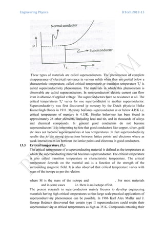
14.1 Magnetic Properties of Superconductors
When the superconducting materials are subjected to a strong magnetic field, it will
result in the destruction of the superconducting property. i.e, they return to the normal
state. The minimum field required to destroy the superconducting property is called
the critical field (Hc). The variation of Hc with temperature is as shown.
The equation used in this connection is
14.2 Critical Currents
The readers should recognize that the magnetic field which destroy the
superconducting property need not be the external electrical field, it can be due to the
current flowing through your superconductor. Hence the maximum current flowing
through the specimen at which this property is destroyed is called critical current.
If a superconducting wire of radius r carries a current I, then as per Ampere’s law,
i.e.,](https://image.slidesharecdn.com/engineeringphysics-151212062959/85/Engineering-physics-29-320.jpg)
![Engineering Physics B.Tech:2012-13
The magnetic susceptibility is
߯ெ ൌ
ܯ
ܪ
ൌ െ1 ሾ12.2ሿ
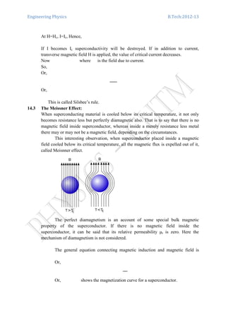
It must be noted that superconductivity is not only a strong diamagnetism but
also a new type of diamagnetism.
14.4 Isotope effect: It is also observed that critical temperature varies with mass of the
isotope as per the relation
ܯఈ
ܶ ൌ ܿݐ݊ܽݐݏ݊
where M is the mass of the isotope and 0.15 ߙ 0.50 . For most materials
ߙ ൌ 0.5 and in some cases ߙ ൌ 0 i.e. there is no isotope effect.
Example:
The critical temperature for mercury with isotopic mass 199.5 is 4.18K. Calculate its
critical temperature when its isotopic mass changes to 203.4.
Solution: The data given in the question are M1 = 199.5, M2 = 203.4 and Tc1 = 4.18 K.
The critical temperature in terms of its isotopic mass is given by
ܶ ൌ ܯܣ
ିଵ
ଶ
Therefore we have,
ܶଵ
ܶଶ
ൌ ൬
ܯଵ
ܯଶ
൰
ି
ଵ
ଶ
ൌ ඨ
ܯଶ
ܯଵ
Or, ܶଶ ൌ ܶଵට
ெభ
ெమ
ൌ 4.18 ൈ ට
ଵଽଽ.ହ
ଶଷ.ସ
ൌ 4.14ܭ
[Reference: Material Science by M. S. Vijaya and G. Rangarajan, Page-325-328]
[Reference: Material Science by V. Rajendran and A. Marikani, Pages-12.2-12.4]
Session-15
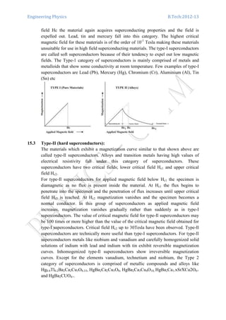
15.1 Types of Superconductors
Superconductors are differentiated by there magnetization curves by two types. They
are
a. TYPE I or soft superconductor
b. TYPE II or hard Super conductor
15.2 Type-I (soft superconductors)
The superconductors in which magnetic field is totally excluded from the interior of
the superconductor below a certain critical magnetic field Hc and at H = Hc the
material looses its superconductivity abruptly and the magnetic field penetrates fully,
are termed as type-I or soft superconductors. Type-I superconductors exhibit Meissner
effect of magnetic flux exclusion. The magnetization curve for type-I superconductors
are shown in Fig. The magnetization curve shows that the transition at H = Hc is
reversible and means that if applied magnetic field is reduced below critical magnetic](https://image.slidesharecdn.com/engineeringphysics-151212062959/85/Engineering-physics-31-320.jpg)
![Engineering Physics B.Tech:2012-13
A distinguishing characteristic of type-I and type-Il superconductors is provided by a
modification of the Meissner effect in type-Il superconductors as shown in fig. This
figure illustrates that superconductivity is only partially destroyed in type-II
superconductors for . The state of the specimen in this region is
called vortex state. The vortex state is really a mixture of normal state and
superconducting state. In general vortex state is unstable for type-I superconductors
where as it is stable for type-Il superconductors. The variation of critical magnetic
field with temperature of a type-Il superconducting material is shown in F ig.(b)
15.4 Some Properties of Superconducting materials:
(i) At room temperature, superconducting materials have greater resistivity than other
elements.
(ii) The transition temperature Tc is different for different isotopes of an element. If
decreases with increasing atomic weight of the isotopes.
(iii) The superconducting property of a superconducting element is not lost by
impurities to it but the critical temperature is lowered.
(iv)There is no change in the crystal structure as revealed by x-ray diffraction studies.
This means that superconductivity may be more concerned with the conduction
electrons than with the atoms themselves.
(v) The thermal expansion and elastic properties do not change in the transition.
(vi) All thermoelectric effects disappear in superconducting state.
(vii) When a sufficiently strong magnetic field is applied to a superconductor below
the critical temperature, its superconducting property is destroyed. At any given
temperature below Tc, there is a critical magnetic field Hc such that the
superconducting property is destroyed by the application of a magnetic field. The
value of Hc decreases as the temperature increases.
[Reference: Material Science by V. Rajendran and A. Marikani, Pages-12.4-12.5]
[Reference: Material Science by M. S. Vijaya and G. Rangarajan, Page-329]
Session-16](https://image.slidesharecdn.com/engineeringphysics-151212062959/85/Engineering-physics-33-320.jpg)
![Engineering Physics B.Tech:2012-13
energy the vibrations in the lattice become more violent and break the pairs. As they
break, superconductivity diminishes.
[Reference: Material Science by V. Rajendran and A. Marikani, Pages-12.4-12.5]
Session-17
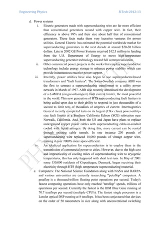
17 Applications of superconductors:
a. Transportation: Magnetic-levitation is an application where superconductors
perform extremely well, Transport vehicles such as trains can be made to "float"
on strong superconducting magnets, virtually eliminating friction between the
train and its tracks. Not only would conventional electromagnets waste much of
the electrical energy as heat, they would have to be physically much larger than
superconducting magnets. A landmark for the commercial use of MAGLEV
technology occurred in 1990 when it gained the status of a nationally-funded
project in Japan. The Minister of Transport authorized construction of the
Yamanashi Maglev Test Line which opened on April 3, 1997. In December 2003,
the MLX01I test vehicle attained an incredible speed of 361 mph (581 km/hr).
b. Medical:
i. An area where superconductors can perform a life-saving function is in the
field of bio magnetism. Doctors need a non-invasive means of determining
what's going on inside the human body. By impinging a strong
superconductor-derived magnetic field into the body, hydrogen atoms that
exist in the body's water and fat molecules are forced to accept energy
from the magnetic field. They then release this energy at a frequency that
can be detected and displayed graphically by a computer.
ii. The Korean Superconductivity Group has carried bio magnetic technology
a step further with the development of a double-relaxation oscillation
SQUID (Superconducting Quantum. Interference Device) for use in
Magnetoencephalography. SQUID's are capable of sensing a change in a
magnetic field over a billion times weaker than the force that moves the
needle on a compass. With this technology, the body can be probed to
certain depths without the need for the strong magnetic fields associated
with MRl's.
c. Fundamental Research
i. Josephson Effect in superconductivity resulted in an upward revision of
Planck's constant from 6.62559 x 10⁻³⁴
to 6.626196 X 10⁻³⁴
.
ii. Superconductivity has become an essential tool in research work relating
to elementary particle which will ultimately lead to the door of creation of
the universe. High-energy particle research hinges on being able to
accelerate sub-atomic particles to nearly the speed of light. Superconductor
magnets make this possible. CERN, a consortium of several European
nations, is constructing Large Hadron Collider (LHC).](https://image.slidesharecdn.com/engineeringphysics-151212062959/85/Engineering-physics-35-320.jpg)
![Engineering Physics B.Tech:2012-13
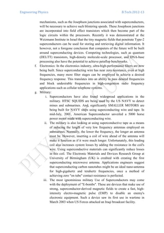
h. Space Research: Among emerging technologies are a stabilizing momentum
wheel (gyroscope) for earth-orbiting satellites that employs the "flux-pinning"
properties of imperfect superconductors to reduce friction to near zero.
Superconducting x-ray detectors and ultra-fast, superconducting light detectors
are being developed due to their inherent ability to detect extremely weak
amounts of energy; Already Scientists at the European Space Agency (ESA)
have developed what's being called the "S-Cam", an optical camera of
phenomenal sensitivity.
i. Internet: Superconductors may even play a role in Internet communications
soon. Superconductivity can be used to develop a superconducting digital
router for high-speed data communications up to 160 GHz. Since Internet
traffic is increasing exponentially, superconductor technology is being called
upon to meet this super need.
j. Pollution Control: Another impetus to the wider use of superconductors is
political in nature. The reduction of green-house gas (GHG) emissions has
becoming a topical issue due to the Kyoto Protocol which requires the
European Union (EU) to reduce its emissions by 8% from 1990 levels by
2012. Physicists in Finland have calculated that the EU could reduce carbon
dioxide emissions by up to 53 million tons if high-temperature
superconductors were used in power plants.
k. Refrigeration: The future melding of superconductors into our daily lives will
also depend to a great degree on advancements in the field of cryogenic
cooling. New, high-efficiency magnetocaloric-effect compounds such as
gadolinium-silicon-germanium are expected to enter the marketplace soon.
Such materials should make possible compact, refrigeration units to facilitate
additional HTS applications.
[Reference: Material Science by V. Rajendran and A. Marikani, Pages-12.8-12.10]
[Reference: Material Science by M. S. Vijaya and G. Rangarajan, Page-352-353]
Session-18
Assignment-1
Module-II
Session-19
Optical Materials:
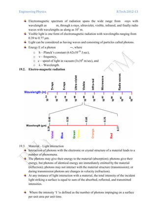
19.1. Optical properties
Optical property of a material is defined as its interaction with electro-magnetic
radiation in the visible range.](https://image.slidesharecdn.com/engineeringphysics-151212062959/85/Engineering-physics-38-320.jpg)
![Engineering Physics B.Tech:2012-13
19.4. Optical materials
Materials are classified on the basis of their interaction with visible light into three
categories.
Materials that are capable of transmitting light with relatively little absorption and
reflection are called transparent materials i.e. we can see through them.
Translucent materials are those through which light is transmitted diffusely i.e.
objects are not clearly distinguishable when viewed through.
Those materials that are impervious to the transmission of visible light are termed as
opaque materials. These materials absorb all the energy from the light photons.
19.5. Optical properties – Metals
Metals consist of partially filled high-energy conduction bands.
When photons are directed at metals, their energy is used to excite electrons into
unoccupied states. Thus metals are opaque to the visible light.
Metals are, however, transparent to high end frequencies i.e. x-rays and γ-rays.
Absorption of takes place in very thin outer layer. Thus, metallic films thinner than
0.1 µm can transmit the light.
The absorbed radiation is emitted from the metallic surface in the form of visible light
of the same wavelength as reflected light. The reflectivity of metals is about 0.95,
while the rest of impinged energy is dissipated as heat
The amount of energy absorbed by metals depends on the electronic structure of each
particular metal. For example: with copper and gold there is greater absorption of the
short wavelength colours such as green and blue and a greater reflection of yellow,
orange and red wavelengths.
[Reference: Material Science by V. Rajendran and A. Marikani, Pages-13.1-13.3]
[Reference: Material Science by M. S. Vijaya and G. Rangarajan, Page-461-462]
Session-20
20.1 Optical properties of non-metallic materials
Non-metallic materials consist of various energy band structures. Thus, all four
optical phenomena such as absorption, reflection, transmission and refraction are
important for these materials.
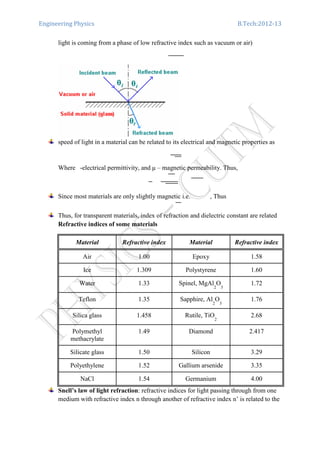
20.2 Refraction
When light photons are transmitted through a material, they cause polarization of the
electrons and in-turn the speed of light is reduced and the beam of light changes
direction.
The relative velocity of light passing through a medium is expressed by the optical
property called the index of refraction (n), and is defined as
݊ ൌ
ܿ
ݒ
where c – speed of light in vacuum, v – speed of light in the concerned material.
If the angle of incidence from a normal to the surface is θi, and the angle of refraction
is θr, the refractive index of the medium, n, is given by (provided that the incident](https://image.slidesharecdn.com/engineeringphysics-151212062959/85/Engineering-physics-40-320.jpg)
![Engineering Physics B.Tech:2012-13
Tyndall effect is where scattering occurs from particles much larger than the
wavelength of light. Ex.: Clouds look white.
Compton scattering: interacting photon knocks out an electron loosing some of its
energy during the process. This is also significant for high atomic number atoms and
low photon energies.
Photoelectric effect occurs when photon energy is consumed to release an electron
from atom nucleus. This effect arises from the fact that the potential energy barrier for
electrons is finite at the surface of the metal. Ex.: Solar cells.
20.6 Transmission
Fraction of light beam that is not reflected or absorbed is transmitted through the
material.
The process of light transmission is as follows
[Reference: Material Science by V. Rajendran and A. Marikani, Pages-13.3]
[Reference: Material Science by M. S. Vijaya and G. Rangarajan, Page-462, 466, 468]
Session-21
21.1 LASER
The absorption and emission of electromagnetic radiation by materials has been very
ingeniously and skill fully exploited in making a device that amplifies
electromagnetic radiation and generates extremely intense, coherent and mono-
chromatic radiation. This device is called LASER. The term laser is acronym for
Light Amplification by Stimulated Emission of Radiation.
When light radiation of suitable wavelength to match the energy levels in a material is
incident on the material, the electrons absorb the radiation and get excited to higher
energy levels.](https://image.slidesharecdn.com/engineeringphysics-151212062959/85/Engineering-physics-43-320.jpg)
![Engineering Physics B.Tech:2012-13
frequencies. Or in other words the radiation is- not perfectly monochromatic. It will
have a small broadening. This is illustrated in Fig. 22.1.
[Reference: Material Science by M. S. Vijaya and G. Rangarajan, Page-484-486]
Session-22
22.1 Broadening of Emitted Radiation
The emitted radiation from the laser has a finite broadening. One reason for the
broadening is the inherent width of the energy levels. According to Heisenberg's
uncertainty principle, there is an uncertainty ∆ܧ in the determination of the energy of
an energy level given by the relation
∆ݐ∆ ܧ ൌ ݄ Where ∆ݐ is the time of measurement or can be interpreted as the
lifetime of the atom in the energy level E. ∆ܧ is the inherent or the natural width of
the energy level. If ∆ܧ is small, i.e. if the energy level is sharp then the life time ∆ݐ is
large from the uncertainty relation. This means that the energy level in which the
lifetime of the atom is large is very sharp and those energy levels in which the life
time is short are broad. Since in the ground state the atom is most stable, the lifetime
in the ground state energy level is large and so it follows that the ground state energy
level is very sharp. The higher energy levels have a characteristic life time and hence
corresponding characteristic width. The width of the energy level is given by ∆ܧ ≅
∆ݐൗ . This inherent width ofthe upper energy levels results in finite broadening of the
emitted light as described in Fig.( 22.1). This broadening is called the natural
broadening.
Some of the other broadening mechanisms are:
• Collisional broadening
• Doppler broadening
22.2 Collisional broadening is due to the collision of the excited atom with the atoms,
molecules or electrons which are in the immediate surrounding of the excited atom.
Due to the collisions the atom may lose energy and decay to the lower energy level.
The atom may come to the lower energy state even earlier than its natural life time.
This causes increase in the uncertainty ∆ܧ and hence broadening of the emitted light.
22.3 Doppler broadening is due to the constant motion of the atoms in the laser medium.
This effect is more pronounced in gas lasers. Due to the motion of the atom, while the
atom decays to a lower energy level, there will be shift in the frequency of the emitted
radiation. The shift depends on the velocity. This is the well-known Doppler Effect.
Due to the random motion of the atoms, there will be a small distribution in the
frequency of the emitted radiation about the actual emitted frequency ߥ. This is
called Doppler broadening. The Doppler broadening is normally larger than the
natural broadening.
22.4 Coherence
Laser is a coherent source of radiation. This means that the waves that are
emanating from the laser have the same frequency and they are all in phase with each](https://image.slidesharecdn.com/engineeringphysics-151212062959/85/Engineering-physics-46-320.jpg)
![Engineering Physics B.Tech:2012-13
P
Q
s a
b
݈௧
r
Spatial coherence is also called lateral or transverse coherence. This refers to the
lateral distance between two waves coming out of the source. Consider two waves
coming out of the source from the portions P and Q as shown in Fig.
Let the lateral distance between the two portions be s. The two waves will be in
phase as they emanate from the source. As the waves travel away from the source the
lateral distance between the two waves increases as shown. The phase difference will
be maintained up to a certain distance, say r, at which the lateral distance is ݈௧ .
Beyond this they go completely out of phase. The distance ݈௧ is called the spatial
coherence length and it is related to r and s by
݈௧ ൌ
ߣݎ
ݏ
Where ߣ is the wavelength of the source.
[Reference: Material Science by M. S. Vijaya and G. Rangarajan, Page-487-489]
Session-23
23.1 Necessary Condition for Laser Action -
23.1.1 Population Inversion
We have seen that an incident photon causes induced absorption and induced
emission. The probability of both absorption and emission are equal. So in the
presence of radiation there will be continuous transitions between the two states, i.e.
continuously the energy (photons) is being absorbed and emitted. The photons that are
emitted due to the transition from upper to the lower level cause further transition
from the lower to the upper level and thus they tend to get continuously absorbed in
the laser medium. The absorption process for an input radiation of intensity ܫ
travelling in the Z-direction in the medium is described by the equation
ܫ ൌ ܫ݁ሾఙೠሺேೠିேሻ௭ሿ
ሾ23.1ሿ
where Nu and NI are the population of the upper and the lower level respectively,
and a is called the stimulated emission cross section and it is a characteristic
parameter which depends on the transition probability between the two states. Under](https://image.slidesharecdn.com/engineeringphysics-151212062959/85/Engineering-physics-48-320.jpg)
![Engineering Physics B.Tech:2012-13
normal conditions the lower level is more populated than the upper level and the
exponent in Eq. (23. 1) is negative and this describes the absorption process. But if the
value of the exponent in the equation is positive, then ܫ ܫ, i.e. the radiation will get
amplified instead of getting attenuated! So amplification will occur if ܰ௨ ܰ i.e. if
the upper level is more populated than the lower level. Thus population inversion is a
necessary condition for amplification of stimulated radiation.
Population inversion is a necessary condition but not a sufficient condition for
laser action
23.1.2 How to Achieve Population Inversion in a Laser Medium?
Consider a laser system with two energy levels. Initially the lower level is much
more highly populated than the upper level, i.e. ܰ௨ ൏ ܰ so that we can assume that
ܰ ൌ ܰ௨ ܰ ≅ ܰ where N is the total number of atoms in the two level systems.
Suppose now a radiation of intensity ܫ is made to pass through the system, the
energy is absorbed by the system. The intensity of the beam coming out of the system
of length L is given by (replacing ሺܰ௨ െ ܰሻ ≅ െܰ by -N, and z by L in Eq. (23.1)):
ܫ ൌ ܫ݁ሾିఙೠேሿ
As lo is increased (i.e. as the input intensity is increased) the energy absorbed in
the medium l increases. The photons absorbed cause transition of atoms from lower
level to the upper level. For very high intensities, there will be large number of
photons, and so it appears that all the atoms in the lower level would get transferred to
the upper level. Thus with very high intensities it appears that population inversion
could be achieved! But this does not really happen because of the following reason:
We can rewrite Eq. (23.1) (putting ܰ௨ ൌ ܰ െ ܰ )as
ܫ ൌ ܫ݁ሾఙೠሺேିଶேሻሿ
ܫ ,ݎ ൌ ܫ݁ሾఙೠቀଵିଶ
ே
ே
ቁேሿ
ሾ23.2ሿ
Initially all the atoms are in the lower level so the ratio
ே
ே
ൌ 1 . As the atoms in
the lower level are pumped to the upper level, ܰ decreases, so that the ratio
ே
ே
drops
from unity. As it decreases and reaches the value 0.5, I in Eq. (23.2) becomes equal to
ܫ, That is, there can be no more absorption, when the two levels have equal
population! But due to the mechanisms of spontaneous emission and induced
emission there will be a continuous transition from upper level to lower level and this
leads to further absorption. Thus
ே
ே
will never decrease to a value less than 0.5. The
conclusion is that population inversion cannot be achieved between two energy levels
by just optical pumping between the same two levels. A minimum of three energy
levels are involved in population inversion and laser action.
[Reference: Material Science by M. S. Vijaya and G. Rangarajan, Page-489-491]
Session-24
24.1 Saturation Intensity and Optical Cavity](https://image.slidesharecdn.com/engineeringphysics-151212062959/85/Engineering-physics-49-320.jpg)
![Engineering Physics B.Tech:2012-13
The number of modes within the bandwidth can be obtained by dividing the
emission line width of the beam by . Normally the line width of the laser beam is in
the range of to Hz for various types of lasers and so it can be verified that
there will be a few to several equally spaced resonant lines in the laser output.
[Reference: Material Science by M. S. Vijaya and G. Rangarajan, Page-491-493]
Session-25
25.1 Sufficient Condition for Laser Action - 3 Level Laser
A minimum of three energy levels are required to cause population inversion
between two levels. The ground state is the most populated and stable state. The life
time of an atom in the ground state may be said to be nearly infinity. Upper energy
levels are normally unstable, in the sense that the atoms in those states have very short
life time. They drop down to lower energy states almost instantaneously. To cause
population inversion what is required is an upper energy level which has a reasonably
long life time. Such a state is called a metastable state. A metastable higher energy
level is an essential requirement for laser action. So, a ground state or a lower energy
state, an upper energy state and an intermediate metastable state are the three essential
states for causing population inversion and hence laser action.
This can be understood by considering a three level system shown in Fig
Fig.
The key to laser action is the presence of a broad energy level (with a short life-
time) above the ground state and a third intermediate sharper metastable level with a
longer life time.
The ground state E1 is highly populated and the excited states are sparsely
populated. To cause population inversion the system is irradiated with an intense
radiation so that atoms from the ground state may be pumped to the upper state E2.
This is called optical pumping. Since this energy level is broad, the incident radiation
may be broad band light with a range of frequencies. The lifetime of the atoms in
level E2 is very short (= 10-7
sec) and so the atoms drop down rapidly to the meta-
stable state E3. The transition from E2 to E3 is a non-radiative transition, i.e. it does
not cause emission of radiation. The energy lost is absorbed by the phonons and the](https://image.slidesharecdn.com/engineeringphysics-151212062959/85/Engineering-physics-52-320.jpg)
![Engineering Physics B.Tech:2012-13
system gets heated up. Level E3 has a longer life time of about 10-3
sec. So, with
continuous optical pumping a stage will be reached when the level E3 gets much more
highly populated than the ground state E1. Thus population inversion is achieved
between the levels E3 and E1. What is now required is an incident photon of frequency
that matches the difference in energy levels, i.e. photon of frequency given by
ߥଵଷ ൌ
ሺܧଷ െ ܧଵሻ
݄
ൗ
Spontaneous emission from E3 to E1 will generate the required photons. These
photons stimulate or induce transitions between E3 and E1. The photons emitted by the
transition move within the optical cavity and induce further transitions resulting in an
avalanche of photons as described earlier. All the photons travelling along or close to
the axis of the optical cavity will be emitted out as a highly intense, coherent and
monochromatic radiation of frequency ߥଵଷ.
For laser action to take place continuously, the population inversion between the
two levels must be constantly maintained. As the atoms drop down to the lower state
from the meta-stable state, the difference in population would decrease, if the
pumping rate is not sufficient. So it is essential to maintain a proper pumping rate to
maintain a high population constantly in the meta-stable state. This requires a highly
intense input pumping radiation.
25.2 4 Level Laser
Practical lasers are either 3-level or 4- level lasers. In the four level lasers, the
laser action takes place between the meta-stable state and an intermediate state (E4)
above the ground state. The advantage of 4-level laser is that the maintenance of
population inversion between the meta-stable state and the lower energy state is much
easier because the state E4 has short lifetime and the atoms fall to the ground state
quite rapidly from this state. So a modest pumping rate would be sufficient. Practical
lasers are either continuous or pulsed. Some practical laser systems are described in
the following sections.
[Reference: Material Science by M. S. Vijaya and G. Rangarajan, Page-493-495]
Session-26
26.1 Examples of Laser Systems
Energy Levels For practical lasers, systems with suitable energy levels must be
selected. Lasers have been made with gases, liquids and solids. The energy levels
involved in laser action may be atomic energy levels (e.g. He-Ne, Ruby, Nd-YAG
lasers), molecular vibrational energy levels (e.g. CO2, Dye lasers) or energy bands
(e.g. semiconductor diode lasers). This section describes the energy levels and the
notation used for the levels, in different types of lasers.](https://image.slidesharecdn.com/engineeringphysics-151212062959/85/Engineering-physics-53-320.jpg)
![Engineering Physics B.Tech:2012-13
spaced and the separation is in the range of middle infra-red. In each electronic state
the molecules may exist in one of several vibrational energy states as shown in Fig.
In addition to the vibrational motion, molecules rotate about specific molecular
axes. The rotational energy of the molecules is given by
where J, called the angular momentum quantum number takes integer values (J
should not be confused with the atomic angular momentum quantum number; here we
are talking about molecular angular momentum). The rotational energy levels are not
equally spaced. The separation between the rotational states lies in the far infra-red or
in the microwave range. Figure shows the rotational energy levels which lie closely
between vibrational energy levels. Transitions between the energy levels are possible
governing certain rules known as selection rules. Selection rules for rotational energy
levels is for vibrational energy levels .
[Reference: Material Science by M. S. Vijaya and G. Rangarajan, Page-495-497]
Session-27
27.1 Ruby Laser
Ruby laser is a single crystal of AI2O3 doped with chromium. Cr3+
ions replace
some of the Al3+
ions in the crystal. The Cr3+
ions are responsible for the red colour of
ruby. The laser action takes place in chromium ion energy levels. The schematic
diagram of ruby laser is shown Fig. A single crystal of ruby (Al2O3 + Cr3+
) in the
form of a rod is the laser system. The two ends of the rod are ground perfectly
parallel. A total reflective mirror is placed parallel and closed at one end of the rod
and a partially reflecting mirror is placed at the other end as shown. For optical
pumping, a high intensity xenon flash lamp is used. The xenon lamp is in the form of](https://image.slidesharecdn.com/engineeringphysics-151212062959/85/Engineering-physics-55-320.jpg)
![Engineering Physics B.Tech:2012-13
a spiral and the ruby rod is placed along the axis of the spiral lamp. The ruby rod is
enclosed in a tube and is cooled by circulating a coolant through the tube.
Ruby laser is a three-level laser system. Cr3+
ions have three energy levels as
shown in Fig.
An intense radiation of wavelength in the range 5500 emitted from the xenon
flash lamp is used for exciting Cr3+
ions from the ground state to the excited state
which has a short life time. The excited ions soon fall to the metastable state and this
transition is a non-radiative transition. This change in energy is absorbed by the
phonons and the crystal gets heated up. Soon population inversion is achieved
between the meta-stable state and the ground state. Spontaneous emission due to
transition from the meta-stable state generates photons of energy 1.79 eV (6943 ).
These photons are reflected back and forth between the mirrors at the ends of the ruby
rod. The photons stimulate transitions from the metastable state to the ground state.
The photons emitted through stimulation will be in phase with the stimulating
photons.
[Reference: Material Science by M. S. Vijaya and G. Rangarajan, Page-497-498]
Session-28
28.1 Applications of Laser
The advent of lasers opened up a wide vista of new techniques of materials study and
materials processing and generated new innovations in high precision measurements.
Lasers find applications in almost all fields of science and technology. The special](https://image.slidesharecdn.com/engineeringphysics-151212062959/85/Engineering-physics-56-320.jpg)
![Engineering Physics B.Tech:2012-13
Lasers in precision measurement: Laser interferometry techniques are used for
precise measurement of thickness of very thin fibres and thin films. Small
displacements may be measured with an accuracy of . He-Ne lasers or
semiconductor lasers are used in these applications as high power is not required.
Other applications of lasers include holography and laser spectroscopy.
Holography is the technique of capturing three dimensional images of objects. In
conventional photography, what is recorded is only the intensity pattern of the object
and so the photographic image is a two dimensional recording of the object. In
holography, in addition to the intensity, the relative phase of the waves coming from
different parts of the body is also recorded which results in a three dimensional image.
[Reference: Material Science by M. S. Vijaya and G. Rangarajan, Page-504-502]
Session-29
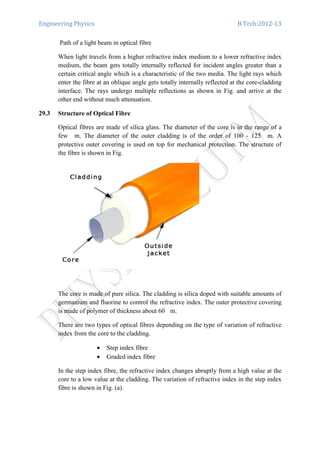
29.1 OPTICAL FIBRES
Optical fibres are waveguides that carry optical radiation. They are thin long flexible
fibres made of silica (glass). If a light source is placed close to one end, the light
radiation is transmitted to the other end of the fibre with little loss, even if the fibre is
bent or coiled!
Optical fibres are used in modem optical communication. The fibre can carry light
signals over long distances without much attenuation and distortion. In optical
communication, the electrical signals are encoded into light signals and the modulated
light signal from the transmitter (semiconductor laser) is transmitted through long
optical fibres and at the other end of the fibre a photodiode converts light signals back
to electrical signals.
29.2 Principle of Optical Fibre
The optical fibre is a thin long glass wire with a composite structure. The central part
called the core is made of high refractive index glass and the surrounding region
called the cladding is made of lower refractive index material. The light beam that
enters the fibre at one end will be confined to travel within the core region because of
total internal reflection at the interface between the two types of glasses. This can be
understood from Fig.](https://image.slidesharecdn.com/engineeringphysics-151212062959/85/Engineering-physics-58-320.jpg)
![Engineering Physics B.Tech:2012-13
In this type of fibre, the various light beams entering the fibre at different angles will
traverse different total distances before they arrive at the other end of the fibre as
shown in Fig. (a). So they reach the end at slightly different instances of time. As a
result the modulated light pulse which passes through the fibre will get slightly
distorted when it comes out of the fibre.
In graded index fibre, the distortion is minimized by making the variation of the
refractive index gradual from the axis of the core. The refractive index has a parabolic
variation with its maximum at the fibre axis as shown in Fig. (b). In this type of fibre
the velocity of light is greater near the periphery than at the axis. So those beams
which traverse longer paths in the fibre travel faster in the lower index material and
arrive at the output at the same time as the beam that passes nearer to the axis where
the index is higher. This minimizes the distortion of the signal arriving at the end of
the fibre. The path of the light beam in the graded optical fibre is shown in Fig. (b).
Very thin optical fibres (2 - 8 m diameter) which transmit only one mode are called
mono-mode fibres. Thicker fibres (about 50 m diameter) can transmit several modes
and they are called multi-mode fibres.
[Reference: Material Science by M. S. Vijaya and G. Rangarajan, Page-506-508]
Session-30
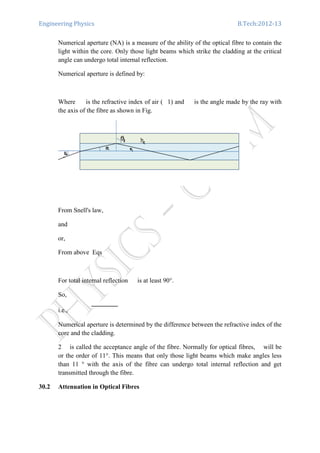
30.1 Numerical Aperture of a Step Index Fibre](https://image.slidesharecdn.com/engineeringphysics-151212062959/85/Engineering-physics-60-320.jpg)
![Engineering Physics B.Tech:2012-13
The light signal, as it travels through the fibre, there is a loss of optical power, which
is called attenuation. Signal attenuation is defined as the ratio of optical input power
(Pi) to the optical output power (Po). Optical input power is the power transmitted into
the fibre from an optical source. Optical output power is the power received at the
fibre end. So, the signal attenuation or absorption coefficient is defined as:
ߙ ൌ
10
ܮ
logଵ
ܲ
ܲ
Where L is the length of the fibre.
The sources of attenuation are:
• energy absorption by lattice vibrations of the ions of the glass material
• Energy absorption by impurities in the glass. The impurities are mainly
hydroxyl ions which get introduced during fibre production at high
temperature.
• Scattering of light due to local variation in the refractive index. The
unintentional local variations arise due to disordered structure of the glass.
All the above processes are wavelength dependent. By choosing a proper wavelength
of the light signal where the absorption and scattering is minimum due to the above
processes, attenuation may be minimized. The best suited wave lengths for SiO2-
GeO2 glasses are 1310 nm and 1550 nm.
[Reference: Material Science by M. S. Vijaya and G. Rangarajan, Page-508-509]
Session-31
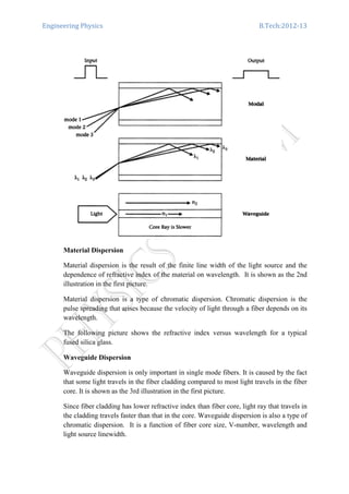
31.1 Pulse dispersion
Dispersion is the spreading out of a light pulse in time as it propagates down the fiber.
Dispersion in optical fiber includes model dispersion, material dispersion and
waveguide dispersion. Each type is discussed in detail below.
Modal Dispersion in Multimode Fibres
Multimode fibres can guide many different light modes since they have much larger
core size. This is shown as the 1st illustration in the picture above. Each mode enters
the fibre at a different angle and thus travels at different paths in the fibre.
Since each mode ray travels a different distance as it propagates, the ray arrives at
different times at the fibber output. So the light pulse spreads out in time which can
cause signal overlapping so seriously that you cannot distinguish them any more.
Model dispersion is not a problem in single mode fibres since there is only one mode
that can travel in the fibre.](https://image.slidesharecdn.com/engineeringphysics-151212062959/85/Engineering-physics-62-320.jpg)
![Engineering Physics B.Tech:2012-13
While the difference in refractive indices of single mode fiber core and cladding are
minuscule, they can still become a factor over greater distances. It can also combine
with material dispersion to create a nightmare in single mode chromatic dispersion.
Various tweaks in the design of single mode fiber can be used to overcome waveguide
dispersion, and manufacturers are constantly refining their processes to reduce its
effects.
[Reference: Material Science by M. S. Vijaya and G. Rangarajan,]
Session-32
32.1 Optical Fibre Amplifier
When light signals are transmitted through optical fibres over long distances, there
will be attenuation due to absorption in the path. The signal needs to be amplified for](https://image.slidesharecdn.com/engineeringphysics-151212062959/85/Engineering-physics-64-320.jpg)
![Engineering Physics B.Tech:2012-13
[Reference: Material Science by M. S. Vijaya and G. Rangarajan, Page-511]
Session-33
33.1 Medical applications: Optical fibres are used in endoscopes to get the image of the
particular part of the body.
An endoscope consists of a bunch of optical fibres which carries light to the inside of
body and then transfers an image of the minor parts of the body to be viewed on the
screen by the doctor. Endoscopy can be better being done using laser beams because
of the coherence characteristics.
Endoscope can be inserted in the body through the mouth or rectum and moved along
any part of the body, where a particular defect has to be studied by a doctor.
In laser surgery, optical fibres are used to transmit the laser beam to the point of
interest where surgery is to be done.
In dental surgery, the dentist’s drill often incorporates a fiber optic cable that lights up
the insides of patients’ mouths.
33.2 Industrial applications: In laser processing of materials like drilling, welding and
cutting, the high power laser is located at one place and the laser radiation will be
transmitted to different locations in the shop floor through optical fibre cables.
33.3 As sensors: Optical fibers are used in a wide variety of sensing devices, ranging from
thermometers to gyroscopes. The potential in this field is nearly unlimited because
transmitted light is sensitive to many environmental parameters, including pressure,
sound waves, structural strain, heat and motion. The fibers are especially useful where
electrical effects made ordinary sensors useless, less accurate or even hazardous.
[Reference: Engineering Physics-II, Md. Khan]
Session-35](https://image.slidesharecdn.com/engineeringphysics-151212062959/85/Engineering-physics-66-320.jpg)
![Engineering Physics B.Tech:2012-13
Or, ሬሬԦ∅ ൌ ሾଓ̂
డ∅
డ௫
ଔ̂
డ∅
డ௬
݇ డ∅
డ௭
ሿ -----------eq[35.1]
Where ሬሬԦൌ ሾଓ̂
డ
డ௫
ଔ̂
డ
డ௬
݇ డ
డ௭
ሿ ----------
eq[35.2]
The gradient of a scalar field is the derivative of the scalar function in each direction.
Note that the gradient of a scalar field is a vector field. An alternative notation is to
use the del or nabla operator, f = grad∅ .
35.4 Physical significance of the gradient. At any point the gradient of a function points
in the direction corresponding to that for which the function varies most rapidly. The
magnitude of the gradient vector gives the size of this maximum variation.
In the scalar field consider two level surfaces S1 and S2 very close to each other
characterized by scalar function ∅ and ∅ ݀∅ respectively. Consider two points
ܲሺ,ݔ ,ݕ ݖሻ and ܴሺݔ ݀,ݔ ݕ ݀,ݕ ݖ ݀ݖሻ on S1 and S2 with position vectors ݎԦ and
ݎԦ ݀ݎሬሬሬሬԦ, respectively, with respect to any arbitrary origin O.
Then ܴܲሬሬሬሬሬԦ ൌ ݀ݎሬሬሬሬԦ ൌ ଓ̂݀ݔ ଔ̂݀ݕ ݇݀ݖ -----------
eq[35.3]
Since ∅ ൌ ∅ሺ,ݔ ,ݕ ݖሻ, we have ݀∅ ൌ
డ∅
డ௫
݀ݔ
డ∅
డ௬
݀ݕ
డ∅
డ௭
݀ݖ -----------eq[35.4]
This equation may be written as ݀∅ ൌ ሾଓ̂
డ∅
డ௫
ଔ̂
డ∅
డ௬
݇ డ∅
డ௭
ሿ ∙ ሺ ଓ̂݀ݔ ଔ̂݀ݕ ݇݀ݖሻ
݀∅ ൌ ሬሬԦ∅ ∙ ݀ݎሬሬሬሬԦ -----------eq[35.5]
ߠ
R
Q
P
ܵଵ
݀݊ሬሬሬሬሬԦ
݀ݎሬሬሬሬԦ
ݎԦ
∅
∅ ݀∅
O
ܵଶ](https://image.slidesharecdn.com/engineeringphysics-151212062959/85/Engineering-physics-69-320.jpg)
![Engineering Physics B.Tech:2012-13
The eq[5] expresses change of scalar field with position in terms of its gradient. If ݀݊
denotes the distance along the normal from the point P to the surface S2, we may write
݀݊ ൌ ܲܳ ൌ ݀ߠݏܿ ݎ ൌ ݊ො ∙ ݀ݎሬሬሬሬԦ -----------eq[35.6]
Where ݊ො is a unit vector normal to the surface S1 at P.
As the value of function increases by ݀∅ when we move from P to Q along ܲܳሬሬሬሬሬԦ, we
can write
݀∅ ൌ
డ∅
డ
݀݊ ൌ
డ∅
డ
݊ො ∙ ݀ݎሬሬሬሬԦ -----------eq[35.7]
Combining eq(5) and (7), we have
݀∅ ൌ ሬሬԦ∅ ∙ ݀ݎሬሬሬሬԦ ൌ
డ∅
డ
݊ො ∙ ݀ݎሬሬሬሬԦ -----------eq[35.8]
As ݀ݎሬሬሬሬԦ is arbitrary vector, eq(8) gives
ሬሬԦ∅ ൌ
డ∅
డ
݊ො -----------eq[35.9]
Therefore, ݃∅ ݀ܽݎ ൌ ሬሬԦ∅ ൌ
డ∅
డ
݊ො
Thus ݃∅ ݀ܽݎ is a vector whose magnitude at any point is equal to the rate of change
of ∅ with distance along the normal to the level surface and whose direction is normal
to the level surface at that point.
As
డ∅
డ
݊ො gives the greatest rate of increase of ∅ with respect to space variable, we may
define gradient in general as follow:
The gradient of a scalar function ∅ is a vector whose magnitude at any point is
equal to the maximum rate of change of scalar function ∅ with respect to space
variable and has the direction of that change.
35.5 PROPERTIES OF GRADIENT
If ∅ ܽ݊݀ Ψ are two scalar functions, then
1. ሬሬԦሺ∅Ψሻ ൌ ሺሬሬԦ∅ሻΨ ∅ሺሬሬԦΨሻ
2. ሬሬԦ ቀ
ஏ
ቁ ൌ
ஏሬሬԦିሬሬԦஏ
ஏమ
Example:
1. Find ሬሬԦ∅ where ∅ ൌ ܽݔଶ
ܾݕଶ
ܿ.ݖ Given a, b and c are constants.
Solution:](https://image.slidesharecdn.com/engineeringphysics-151212062959/85/Engineering-physics-70-320.jpg)
![Engineering Physics B.Tech:2012-13
డథ
డ௫
ൌ 2ܽ,ݔ
డథ
డ௬
ൌ 2ܾ,ݕ
డథ
డ௭
ൌ ܿ
ሬሬԦ∅ ൌ ଓ̂
߲∅
߲ݔ
ଔ̂
߲∅
߲ݕ
݇
߲∅
߲ݖ
ൌ ଓ̂2ܽݔ ଔ̂2ܾݕ ݇ܿ
2. Show that ሬሬԦܸሺݎሻ ൌ ̂ݎ
డ
డ
where ̂ݎ is an unit vector along the position vector ݎԦ .
Solution:
ሬሬԦܸሺݎሻ ൌ ଓ̂
߲ܸ
߲ݔ
ଔ̂
߲ܸ
߲ݕ
݇
߲ܸ
߲ݖ
ൌ ଓ̂
߲ܸ
߲ݎ
߲ݎ
߲ݔ
ଔ̂
߲ܸ
߲ݎ
߲ݎ
߲ݕ
݇
߲ܸ
߲ݎ
߲ݎ
߲ݖ
ൌ
߲ܸ
߲ݎ
ሺଓ̂
߲ݎ
߲ݔ
ଔ̂
߲ݎ
߲ݕ
݇
߲ݎ
߲ݖ
ሻ
Since ݎԦ ൌ ଓ̂ݔ ଔ̂ݕ ݇,ݖ ݎ ൌ ሺݔଶ
ݕଶ
ݖଶ
ሻ
ଵ
ଶൗ
So,
డ
డ௫
ൌ
ଵ
ଶ
ሺݔଶ
ݕଶ
ݖଶሻିଵ
ଶൗ ሺ2ݔሻ ൌ
௫
,
Simillarly,
డ
డ௬
ൌ
௬
and
డ
డ௭
ൌ
௭
.
ሬሬԦܸሺݎሻ ൌ
߲ܸ
߲ݎ
ቀଓ̂
ݔ
ݎ
ଔ̂
ݕ
ݎ
݇
ݖ
ݎ
ቁ ൌ
߲ܸ
߲ݎ
ݎԦ
ݎ
ൌ ̂ݎ
߲ܸ
߲ݎ
[Reference: Physics-I by B.B. swain and P. K. Jena, Pages: 211-216]
Session-36
36.1 Divergence of a vector field
The divergence of a vector A is written as ሬሬԦ ∙ ܣԦ or div A and is given by
݀݅ݒ ܣԦ ൌ ሬሬԦ ∙ ܣԦ ൌ ൬ଓ̂
߲
߲ݔ
ଔ̂
߲
߲ݕ
݇
߲
߲ݖ
൰ ∙ ൫ଓ̂ܣ௫ ଔ̂ܣ௬ ݇ܣ௭൯
Or, ሬሬԦ ∙ ܣԦ ൌ
డೣ
డ௫
డ
డ௬
డ
డ௭
Where ܣ௫, ܣ௬ ܽ݊݀ ܣ௬ are the scalar components of A. The resultant quantity is a
scalar.
e.g. if A=3x2yzi+x2z2j+z2k then ሬሬԦ ∙ ܣԦ=6xyz+2z](https://image.slidesharecdn.com/engineeringphysics-151212062959/85/Engineering-physics-71-320.jpg)
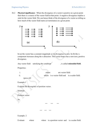
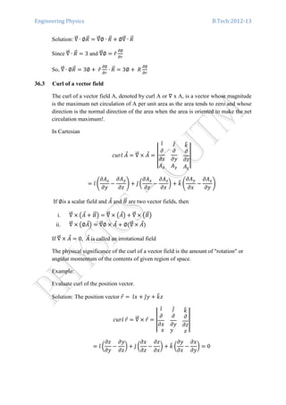
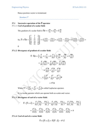
![Engineering Physics B.Tech:2012-13
37.1.5 Divergence of cross product of two vectors:
ሬሬԦ ∙ ൫AሬሬԦ ൈ ܤሬԦ൯ ൌ ܤ ∙ሬሬሬሬሬԦ ൫ሬሬԦ ൈ ܣԦ൯ െ ܣԦ ∙ ൫ሬሬԦ ൈ ܤሬԦ൯
[Reference: Physics-I by B.B. swain and P. K. Jena, Pages: 216-220]
37.2 Line, Surface and Volume integral of vector field
37.2.1 Line integral of vectors: The line integral of a vector field ܣԦ, between two points a
and b, along a given path is
ܫ ൌ න ܣԦ
∙ ݈݀ሬሬሬԦ
Where ݈݀ሬሬሬԦ is a vector length element along the given path between a and b. The line
integral of a vector field is a scalar quantity. In terms of the Cartesian components, the
line integral can be written as
ܫ ൌ න൫ଓ̂ܣ௫ ଔ̂ܣ௬ ݇ܣ௭൯
∙ ሺ ଓ̂݀ݔ ଔ̂݀ݕ ݇݀ݖሻ
ൌ නሺܣ௫݀ݔ ܣ௬݀ݕ ܣ௭݀ݖሻ
If the integral is independent of the path of integration and depends only on the initial
and final points, the corresponding vector field is called a conservative field. The line
integral of a conservative field ܣԦ along a closed path vanishes, i.e.,
ර AሬሬԦ ∙ ݈݀Ԧ
ൌ 0
37.2.2 Physical Significance of line integral:
If ܨԦ is a force and ݈݀ሬሬሬԦ is the small displacement along the path of the particle, the line
integral ܨԦ
∙ ݈݀ሬሬሬԦ represents the work done in moving the particle from point a to
point b along the path in the force field specified by ܨԦ.
37.3 Surface integral of Vectors:
The Surface integral of a vector field AሬሬԦ, over a given surface SሬԦ is
ܫ௦ ൌ න ܣԦ
∙ ݀ܵሬሬሬሬԦ
where dSሬሬሬሬԦ is a vector area element on the surface. The direction of ݀ܵሬሬሬሬԦ is along the
outward normal to the surface. The surface integration may be open or closed. If ݊ො is
a unit vector normal to the surface at the given point, ݀ܵሬሬሬሬԦ=݊ො݀ܵ. So, the surface integral
can be written as](https://image.slidesharecdn.com/engineeringphysics-151212062959/85/Engineering-physics-75-320.jpg)
![Engineering Physics B.Tech:2012-13
ܫ௦ ൌ න ܣԦ
௦
∙ ݊ො݀ܵ ൌ න ܣ݀ܵ
௦
where ܣ ൌ ܣ ∙ ݊ො is the normal component of the vector at the area element.
The surface integral of a vector field is a scalar quantity.
The surface integral of EሬሬԦ i.e., ܧሬԦ
ௌ
∙ ݀ܵሬሬሬሬԦ represents the total electric flux of the electric
field passing through the surface.
For a closed surface the surface integral is written as ∮ AሬሬԦ ∙ ݀ܵሬሬሬሬԦ
௦
37.4 Volume integral of a vector field:
The volume integral of a vector field AሬሬԦ over a given volume V is ܫ௦ ൌ ܣԦ
ܸ݀ where
dV is the differential volume element. The volume integral of a vector is a vector
field.
[Reference: Physics-I by B.B. swain and P. K. Jena, Pages: 220-222]
Session-38
38.1 Gauss divergence theorem:
The theorem states that the volume integral of divergence of a vector ܣԦ over a given
volume V is equal to the surface integral of a vector field over any closed surface
enclosing the volume.
න ሬሬԦ ∙ ܣԦ
௩
ܸ݀ ൌ ර AሬሬԦ ∙ ݀ܵԦ
௦
Example:
Using Gauss divergence theorem, Show that the volume of a sphere is
ସ
ଷ
ߨܴଷ
, where R
is the radius vector.
Proof: Let ܴሬԦ ൌ ଓ̂ݔ ଔ̂ݕ ݇ݖ
From Gauss divergence theorem,
න ሬሬԦ ∙ ܴሬԦ
௩
ܸ݀ ൌ ර RሬሬԦ ∙ ݀ܵԦ
௦
And
ሬሬԦ ∙ ܴሬԦ ൌ ൬ଓ̂
߲
߲ݔ
ଔ̂
߲
߲ݕ
݇
߲
߲ݖ
൰ ∙ ൫ଓ̂ݔ ଔ̂ݕ ݇ݖ൯](https://image.slidesharecdn.com/engineeringphysics-151212062959/85/Engineering-physics-76-320.jpg)
![Engineering Physics B.Tech:2012-13
ൌ
݀ݔ
݀ݔ
݀ݕ
݀ݕ
݀ݖ
݀ݖ
ൌ 1 1 1 ൌ 3
And RሬሬԦ ∙ ݀ܵԦ ൌ ܴ݀ܵ since radius is perpendicular to surface.
So,
න 3
௩
ܸ݀ ൌ ර ܴ݀ܵ ൌ ܴ න ݀ܵ ൌ ܴ ൈ ܵ ൌ ܴ ൈ 4ߨܴଶ
௦௦
Or,
3ܸ ൌ 4ߨܴଷ
,ݎ ܸ ൌ
4ߨܴଷ
3
38.2 Stoke’s theorem
According to this theorem, the surface integral of the curl of a vector field ܣԦ over a
given area S is equal to the line integral of the vector along the boundary C of the
area.
නሺሬሬԦ ൈ ܣԦሻ
௦
∙ ݀ܵԦ ൌ ර AሬሬԦ ∙ ݈݀Ԧ
Here the closed curve C encloses the area S. For closed surface, there is no boundary,
so C=0. Hence the surface integral of the curl of a vector over a closed surface
vanishes.
38.3 Green’s theorem
For any scalar field ߶ and a vector field ܣԦ, we have, ሬሬԦ ∙ ሺ߶ܣԦሻ ൌ ሬሬԦ߶ ∙ ܣԦ ߶ሬሬԦ ∙ ܣԦ
If ܣԦ ൌ ሬሬԦ߰, where ߰ is a scalar field, then
ሬሬԦ ∙ ൫߶ሬሬԦ߰൯ ൌ ሬሬԦ߶ ∙ ሬሬԦ߰ ߶ሬሬԦ ∙ ሬሬԦ߰ ൌ ሬሬԦ߶ ∙ ሬሬԦ߰ ߶ଶ
߰ ሾ1ሿ
Interchanging ߶ and ߰, in equation [1] we get
ሬሬԦ ∙ ൫߰ሬሬԦ߶൯ ൌ ሬሬԦ߰ ∙ ሬሬԦ߶ ߰ሬሬԦ ∙ ሬሬԦ߶ ൌ ሬሬԦ߰ ∙ ሬሬԦ߶ ߰ଶ
߶ ሾ2
Subtracting eq[2] from eq[1], we get
ሬሬԦ ∙ ൫߶ሬሬԦ߰ െ ߰ሬሬԦ߶൯ ൌ ߶ଶ
߰ െ ߰ଶ
߶
Taking the volume integral, we get](https://image.slidesharecdn.com/engineeringphysics-151212062959/85/Engineering-physics-77-320.jpg)
![Engineering Physics B.Tech:2012-13
න ሬሬԦ ∙ ൫߶ሬሬԦ߰ െ ߰ሬሬԦ߶൯ܸ݀ ൌ නሺ߶ଶ
߰ െ ߰ଶ
߶ሻ
ܸ݀ ሾ3ሿ
Using gauss divergence theorem, LHS of eq[3] can be written as
න ሬሬԦ ∙ ൫߶ሬሬԦ߰ െ ߰ሬሬԦ߶൯ܸ݀ ൌ ර൫߶ሬሬԦ߰ െ ߰ሬሬԦ߶൯ ∙ ݀ܵԦ
ௌ
ሾ4ሿ
Where surface S encloses volume V. So, from eq[3], we get
ර൫߶ሬሬԦ߰ െ ߰ሬሬԦ߶൯ ∙ ݀ܵԦ
ௌ
ൌ නሺ߶ଶ
߰ െ ߰ଶ
߶ሻ
ܸ݀ ሾ5ሿ
This is Green’s theorem for two scalar fields.
[Reference: Physics-I by B.B. swain and P. K. Jena, Pages: 222-224]
Session-39
39 Electric field and Gauss' law
39.1 Coulomb's law
The electrostatic force of attraction or repulsion on a point charge q1 due to another
charge q2 separated by a distance r in vacuum is given by Coulomb's law
ܨԦ ൌ
1
4ߨߝ
ݍଵݍଶ
ݎଶ
̂ݎ
Where ̂ݎ is a unit vector from ݍଶ to ݍଵ and ߝ=electric permittivity of vacuumൌ
8.85 ൈ 10ିଵଶ
ܥଶ
ܰିଵ
݉ଶ
.
The constant
ଵ
ସగఌ
ൌ 9.0 ൈ 10ଽ
ܰ݉ଶ
/ܥଶ
In a medium, Coulomb's law is modified to the form
ܨԦ ൌ
1
4ߨߝ
ݍଵݍଶ
ݎଶ
̂ݎ
where ߝ is the electric permittivity of the medium. ߝ ൌ ߝߝ
Here, ߝ ൌ
ఌ
ఌ
is called the relative permittivity or dielectric constant of the medium. It
is a positive number greater than 1.
39.2 Electric field, electric displacement and electric flux](https://image.slidesharecdn.com/engineeringphysics-151212062959/85/Engineering-physics-78-320.jpg)
![Engineering Physics B.Tech:2012-13
If the charge is distributed in a region, we can write
ݍ௧ ൌ න ߩܸ݀
Where ߩ is the volume charge density (charge per unit volume). From Gauss
divergence theorem, we can write,
ර ܧሬԦ ∙ ݀ܵԦ
௦
ൌ න ሬሬԦ ∙ ܧሬԦ
௩
ܸ݀
So,
න ሬሬԦ ∙ ܧሬԦ
௩
ܸ݀ ൌ
1
ߝ
න ߩܸ݀
Or,
නሺሬሬԦ ∙ ܧሬԦ
௩
െ
ߩ
ߝ
ሻܸ݀ ൌ 0
So, the integrand must vanish.
⇒ ሬሬԦ ∙ ܧሬԦ ൌ
ఘ
ఌ
(Gauss law in vacuum)
This is the differential form of Gauss' law. In terms of electric displacement, the
differential form of Gauss' law is ሬሬԦ ∙ ܦሬሬԦ ൌ ߩ
In medium, ሬሬԦ ∙ ܧሬԦ ൌ
ఘ
ఌ
where ߝ is the electric permittivity of the medium.
[Reference: Physics-I by B.B. swain and P. K. Jena, Pages: 224-229]
Session-40
40.1 MAGNETIC FLUX DENSITY (B)
When a magnetic material is placed in an external magnetic field, it gets magnetized.
The magnetism thus produced in the material is known as induced magnetism and this
phenomenon is referred to as magnetic induction. The magnetic lines of force inside
such magnetized materials are called magnetic lines of induction.
The number of magnetic lines of induction crossing unit area at right angles to the
flux is called the magnetic flux density B. Its unit is the tesla which is equal to I
Wb/m2
.](https://image.slidesharecdn.com/engineeringphysics-151212062959/85/Engineering-physics-81-320.jpg)
![Engineering Physics B.Tech:2012-13
ර ܤሬԦ ∙ ݀ܵԦ
ௌ
ൌ න ሬሬԦ ∙ ܤሬԦ
ܸ݀
Or,
ሬሬԦ ∙ ܤሬԦ ൌ 0 ሾ40.2ሿ
This is the differential form of Gauss' law in magnetism. This law depicts the non-
existence of isolated magnetic poles. This is like a constraint on the magnetic fields.
All magnetic fields must satisfy Eq.(40.2)
[Reference: Physics-I by B.B. swain and P. K. Jena, Pages: 229-230]
Session-41
41.1 Ampere's circuital law
Ampere's circuital law (formulated by Andre Marie Ampere) relates the distribution
of magnetic field along a closed loop with the net electric current enclosed by the
closed loop. According to this law, the line integral of magnetic field along a closed
loop is equal to ߤ times the net electric current enclosed by the loop.
ර ܤሬԦ ∙ ݈݀Ԧ ൌ ߤܫ௧ ሾ41.1ሿ
where C is a closed path enclosing the current, and ܫ௧ is the algebraic sum of the
currents enclosed by the loop C . The closed loop C is called the Amperian loop,
which can be of any shape as long as it encloses the currents. The magnetic field can
be evaluated by choosing a convenient shape of the Amperian loop.
Ampere's circuital law can be expressed in terms of magnetic intensity as follows.
ර ܪሬሬԦ ∙ ݈݀Ԧ
ൌ ܫ௧ ሾ41.2ሿ
In a medium, Eq.(41.1) and (41.2) are modified by replacing ߤby ߤ.
41.2 Ampere's law in differential form
The electric current I through a surface S can be written as
ܫ ൌ න ଔԦ ∙ ݀ܵԦ
ௌ
ሾ41.3ሿ](https://image.slidesharecdn.com/engineeringphysics-151212062959/85/Engineering-physics-83-320.jpg)
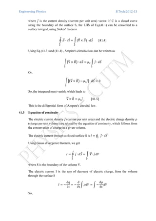
![Engineering Physics B.Tech:2012-13
න ሬሬԦ ∙ ଔԦ
ܸ݀ ൌ න െ
߲ߩ
߲ݐ
ܸ݀
Or,
නሺሬሬԦ ∙ ଔԦ
߲ߩ
߲ݐ
ሻܸ݀ ൌ 0
The vanishing of the integrand gives the equation of continuity,
ሬሬԦ ∙ ଔԦ
߲ߩ
߲ݐ
ൌ 0 ሾ41.6ሿ
The Gauss' law in electrostatics and magnetostatics, and Ampere's circuital law
describe the steady state behavior of the electric and magnetic fields. However, when
the fields change with time, it is observed that (i) a time varying magnetic field gives
rise to electric field and (ii) a time varying electric field produces a magnetic field.
These are described by Faraday's law of electromagnetic induction and Maxwell's
idea of displacement current, respectively.
[Reference: Physics-I by B.B. swain and P. K. Jena, Pages: 231-233]
Session-42
42.1 Faraday's law of electromagnetic induction
Michael Faraday established experimentally that an e.m.f. is induced in a closed
conducting loop if the magnetic flux linked with the surface enclosed by the loop
changes with time. The magnitude of the induced e.m.f. depends on the rate at which
the flux changes. This is depicted quantitatively in Faraday's law of electromagnetic
induction, according to which the e.m.f ࣟ induced in a conducting loop is equal to the
negative of the rate of change of magnetic flux through the surface enclosed by the
loop.
ࣟ ൌ െ
߲∅
߲ݐ
The induced e.m.f. is the line integral of electric field along the loop
ࣟ ൌ ර ܧሬԦ ∙ ݈݀Ԧ
If S is the surface enclosed by the loop, the magnetic flux through the surface area S is](https://image.slidesharecdn.com/engineeringphysics-151212062959/85/Engineering-physics-85-320.jpg)
![Engineering Physics B.Tech:2012-13
∅ ൌ න ܤሬԦ
ௌ
∙ ݀ܵԦ
So, we have
ර ܧሬԦ ∙ ݈݀Ԧ
ൌ െ
߲
߲ݐ
න ܤሬԦ
ௌ
∙ ݀ܵԦ ሾ42.1ሿ
This is Faraday's law of electromagnetic induction in terms of E and B.
42.2 Differential form of Faraday's law
Using Stoke's theorem, the line integral in the LHS of Eq.(42.1 ) can be converted to a
surface integral,
ර ܧሬԦ ∙ ݈݀Ԧ
ൌ න൫ሬሬԦ ൈ EሬሬԦ൯ ∙ ݀ܵԦ
ௌ
Using his equation, we get
න൫ሬሬԦ ൈ EሬሬԦ൯ ∙ ݀ܵԦ
ௌ
ൌ െ
߲
߲ݐ
න ܤሬԦ
ௌ
∙ ݀ܵԦ
Or,
නሺሬሬԦ ൈ EሬሬԦ
߲ܤሬԦ
߲ݐ
ሻ
ௌ
∙ ݀ܵԦ ൌ 0
The vanishing of the integrand gives,
ሬሬԦ ൈ EሬሬԦ
߲ܤሬԦ
߲ݐ
ൌ 0 ሾ42.2ሿ
This is the differential form of Faraday's law of electromagnetic induction.
[Reference: Physics-I by B.B. swain and P. K. Jena, Pages: 233-234]
Session-43
43.1 Maxwell's displacement current
The conduction current (in metals) and convection current (in electrolytic solutions
and ionized gases) produce observable magnetic fields which can be evaluated by
using Biot-Savart law or Ampere's circuital law. However, when the electric field in a](https://image.slidesharecdn.com/engineeringphysics-151212062959/85/Engineering-physics-86-320.jpg)
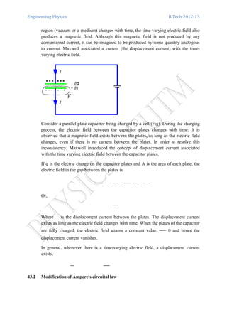
![Engineering Physics B.Tech:2012-13
depends on the frequency with which the electric field alternates. For a copper
conductor in vacuum, the ratio is of the order
ଵభవ
ఠ
. So, for most of the conductors, the
ratio is very large even for reasonably high frequencies. However, if the frequency
exceeds 1020
Hz, the displacement current is dominant. So, the normal conductors
behave as dielectric at extremely high frequencies.
[Reference: Physics-I by B.B. swain and P. K. Jena, Pages: 234-237]
Session-44
44.1 Maxwell's electromagnetic equations
The various laws of electromagnetism were pulled together and were cast into four
equations involving time and space derivatives of electric and magnetic fields. These
equations are known as Maxwell's electromagnetic equations and are given below.
ሬሬԦ ∙ ܦሬሬԦ ൌ ߩ (Gauss law in electrostatics) [44.1]
ሬሬԦ ∙ ܤሬԦ ൌ 0 (Non existence of isolated magnetic pole) [44.2]
ሬሬԦ ൈ EሬሬԦ
డሬԦ
డ௧
ൌ 0 (Faraday's law of e.m. induction) [44.3]
ሬሬԦ ൈ ܪሬሬԦ െ
డሬሬԦ
డ௧
ൌ ܬԦ (Ampere-Maxwell law) [44.4]
The above four are the famous Maxwell's electromagnetic equations in a medium in
the presence of charges and currents. They are the differential forms of (i) Gauss' law
in electrostatics, (ii) Gauss' law in magnetism, (iii) Faraday's law of electromagnetic
induction and (iv) generalized form of Ampere's circuital law respectively.
(i) Eq.(1) and (2) have the same form in vacuum or in a medium. They are
also unaffected by the presence of free charges or currents. They are
usually called the constraint equations for electric and magnetic fields.
(ii) Eq.(1) and (4) depend on the presence or absence of free charges and
currents, and also on the medium.
(iii) The divergence equations given by Eq.(1) and (2) are called the steady
state equations as they do not involve the time dependence of fields.
(iv) The curl equations given by Eq.(3) and (4) are the time varying equations
as they describe the time dependence of the fields.
(v) Eq.(2) and (3) are called the homogeneous Maxwell equations because
their R.H.S. = 0 always. The Eq.(1) and (4) are called the inhomogeneous
Maxwell equation.
44.2 Maxwell's equations in terms of ࡱሬሬԦ and ሬሬԦ](https://image.slidesharecdn.com/engineeringphysics-151212062959/85/Engineering-physics-89-320.jpg)
![Engineering Physics B.Tech:2012-13
ර ܧሬԦ ∙ ݈݀Ԧ
ൌ െ
߲
߲ݐ
න ܤሬԦ
ௌ
∙ ݀ܵԦ
ර ܤሬԦ ∙ ݈݀Ԧ ൌ ߤ
න ቆܬԦ ߝ
߲ܧሬԦ
߲ݐ
ቇ
ௌ
∙ ݀ܵԦ
In a medium, ߤ and ߝ are replaced by ߤ and ߝ respectively.
44.5 Physical significance of Maxwell's equations
(i) Maxwell's equations incorporate all the laws of electromagnetism, which were
developed from experimental observations and were expressed in the form of
various empirical laws.
(ii) Maxwell's equations lead to the existence of electromagnetic waves, which has
been amply confirmed by experimental observations. These equations are
consistent with all the observed properties of e.m.waves.
(iii) Maxwell's equations are consistent with the special theory of relativity. (It is
'worth mentioning that many other equations in physics are not consistent with the
requirements of special theory of relativity).
(iv) Maxwell's equations are used to describe the classical e.m. field as well as the
quantum theory of interaction of charged particles with e.m. field.
(v) Maxwell's equations provided a unified description of the electric and magnetic
phenomena which were treated independently.
[Reference: Physics-I by B.B. swain and P. K. Jena, Pages: 237-239]
Session-45
45 ELECTROMAGNETIC WAVES
Maxwell's electromagnetic equations lead to the wave equation for electric and
magnetic fields. The electromagnetic waves, characterized by electric and magnetic
field vectors, are usually classified as gamma rays, X-rays, ultraviolet rays, visible
light, infrared rays, microwaves, radio waves etc. depending on their frequencies.
These waves carry energy and momentum, and travel in vacuum with the same speed.
However, in a medium they travel with different speeds and may undergo dispersion,
absorption etc. They undergo reflection and refraction at boundaries of two media.
45.1 Wave equation for ࡱሬሬԦ and ሬሬԦ
Maxwell's electromagnetic equations are a set of four coupled first order partial
differential equations relating space and time derivatives of various components of
electric and magnetic fields. They can be decoupled to obtain the wave equations for](https://image.slidesharecdn.com/engineeringphysics-151212062959/85/Engineering-physics-91-320.jpg)
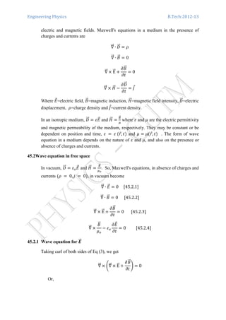
![Engineering Physics B.Tech:2012-13
ሬሬԦ ൈ ሬሬԦ ൈ ܧሬԦ
߲
߲ݐ
൫ሬሬԦ ൈ ܤሬԦ൯ ൌ 0
since the order of space and time derivatives can be interchanged.
Using the vector relation, ሬሬԦ ൈ ሬሬԦ ൈ ܣԦ ൌ ሬሬԦ൫ሬሬԦ ∙ ܣԦ൯ െ ଶ
ܣԦ and eq(4), we get
ሬሬԦ൫ሬሬԦ ∙ ܧሬԦ൯ െ ଶ
ܧሬԦ
߲
߲ݐ
ቆߝߤ
߲ܧሬԦ
߲ݐ
ቇ ൌ 0
This equation involves only ܧሬԦ as ܤሬԦ has been eliminated. Since ሬሬԦ ∙ ܧሬԦ ൌ 0 in free space,
we get
ଶ
ܧሬԦ െ ߝߤ
߲ଶ
ܧሬԦ
߲ݐଶ
ൌ 0 ሾ45.5ሿ
This is the wave equation for ܧሬԦ. Each component of ܧሬԦ satisfies the wave equation,
i.e.,
ଶ
ܧ௫ െ ߝߤ
߲ଶ
ܧ௫
߲ݐଶ
ൌ 0
ଶ
ܧ௬ െ ߝߤ
߲ଶ
ܧ௬
߲ݐଶ
ൌ 0
ଶ
ܧ௭ െ ߝߤ
߲ଶ
ܧ௭
߲ݐଶ
ൌ 0
45.2.2 Wave equation for ሬሬԦ
Similarly the wave equation for ܤሬԦ can be obtained by taking the curl of both sides of
Eq[4],
ሬሬԦ ൈ ሬሬԦ ൈ ܤሬԦ െ ߝߤሬሬԦ ൈ
߲ܧሬԦ
߲ݐ
ൌ 0
Interchanging the order of operation of ሬሬԦ and
డ
డ௧
we get
ሬሬԦ൫ሬሬԦ ∙ ܤሬԦ൯ െ ଶ
ܤሬԦ െ ߝߤ
߲
߲ݐ
൫ሬሬԦ ൈ ܧሬԦ൯ ൌ 0
Using eq(x) and (x), we obtain the wave equation
ଶ
ܤሬԦ െ ߝߤ
߲ଶ
ܤሬԦ
߲ݐଶ
ൌ 0 ሾ45.6 ሿ](https://image.slidesharecdn.com/engineeringphysics-151212062959/85/Engineering-physics-93-320.jpg)
![Engineering Physics B.Tech:2012-13
The wave equations for ܦሬሬԦ and ܪሬሬԦ, in vacuum, have the identical form as that for ܧሬԦ and
ܤሬԦ.
45.3Speed of e.m. wave
We know that the general wave equation satisfied by any wave function ߰ is given by
డమట
డ௫మ
ൌ
ଵ
௩మ
డమట
డ௧మ
, where v is the speed of the wave.
Comparing the wave equations for ܧሬԦ and ܤሬԦ with this, we get the speed of
electromagnetic waves in vacuum,
ݒ ൌ
1
ඥߝߤ
ሾ45.7ሿ
Since ߝ ൌ 8.85 ൈ 10ିଵଶ
݉/ܨ and ߤ ൌ 4ߨ ൈ 10ି
,݉/ܪ the speed of e.m. waves in
vacuum is ݒ ൌ ܿ ൌ 3 ൈ 10଼
݉/,ݏ which is the speed of light in vacuum. The speed of
e.m. waves in vacuum is independent of frequency.
45.4Wave equation in a charge free non conducting medium.
In a charge free, non-conducting medium ߩ ൌ 0 and ܬԦ ൌ 0. If the electric
permittivity ߝ and magnetic permeability ߤ of the medium are independent of position
and time, the wave equation for ܧሬԦ and ܤሬԦ in the medium can be obtained in the same
way as that for free space. The Eq (45.5) and (45.6) take the form in a medium as
ଶ
ܧሬԦ െ ߝߤ
߲ଶ
ܧሬԦ
߲ݐଶ
ൌ 0 ሾ45.8ሿ
And
ଶ
ܤሬԦ െ ߝߤ
߲ଶ
ܤሬԦ
߲ݐଶ
ൌ 0 ሾ45.9ሿ
Since ߝ ߝ and ߤ , the speed of e.m. wave in the medium is
ݒ ൌ
1
√ߝߤ
ሾ45.10ሿ
which is less than c. If ߝ and ߤ are dependent on position and time, the wave equation
becomes more complicated. In a medium, ߝ and ߤ may, in general, depend on
frequency of the wave. So, the speed of e.m. wave in a medium may be different for
different frequencies. Such a medium is called dispersive medium.
[Reference: Physics-I by B.B. swain and P. K. Jena, Pages: 253-257]
Session-46](https://image.slidesharecdn.com/engineeringphysics-151212062959/85/Engineering-physics-94-320.jpg)
![Engineering Physics B.Tech:2012-13
46.1 Wave equation in a charge free conducting medium
In a charge free region ߩ ൌ 0. The electric current density, in a conducting medium is
ܬԦ ൌ ߪܧሬԦ, (from Ohm's law) where ߪ is the conductivity of the medium. If ߝ and ߤ are
independent of position and time, the Maxwell's equation Eq (x) to (x) take the form
ߝሬሬԦ ∙ ܧሬԦ ൌ 0 ሾ46.1ሿ
ሬሬԦ ∙ ܤሬԦ ൌ 0 ሾ46.2ሿ
ሬሬԦ ൈ EሬሬԦ
߲ܤሬԦ
߲ݐ
ൌ 0 ሾ46.3ሿ
ሬሬԦ ൈ
ܤሬԦ
ߤ
െ ߝ
߲ܧሬԦ
߲ݐ
ൌ ߪܧሬԦ ሾ46.4ሿ
Taking the curl of both sides of eq(46.3) and interchanging the order of ሬሬԦ and
డ
డ௧
, we
get,
ሬሬԦ ൈ ሬሬԦ ൈ EሬሬԦ
߲
߲ݐ
ሬሬԦ ൈ ܤሬԦ ൌ 0
Or,
ሬሬԦ൫ሬሬԦ ∙ EሬሬԦ൯ െ ଶ
EሬሬԦ
߲
߲ݐ
ሬሬԦ ൈ ܤሬԦ ൌ 0
Using eq[46.1] and [46.2], in the above, we get
ଶ
EሬሬԦ െ ߝߤ
߲ଶ
ܧሬԦ
߲ݐଶ
ൌ ߤߪ
߲ܧሬԦ
߲ݐ
ሾ46.5ሿ
Similarly, taking the curl of both sides of eq[46.4], we get
ሬሬԦ ൈ ሬሬԦ ൈ ܤሬԦ െ ߝߤሬሬԦ ൈ
߲ܧሬԦ
߲ݐ
ൌ ߪߤሬሬԦ ൈ EሬሬԦ
Or,
ሬሬԦ൫ሬሬԦ ∙ ܤሬԦ൯ െ ଶ
ܤሬԦ െ ߝߤ
߲
߲ݐ
ቆെ
߲ܤሬԦ
߲ݐ
ቇ ൌ െߪߤ
߲ܤሬԦ
߲ݐ
Further, ሬሬԦ ∙ ܤሬԦ ൌ 0, so we get
ଶ
ܤሬԦ െ ߝߤ
߲ଶ
ܤሬԦ
߲ݐଶ
ൌ ߤߪ
߲ܤሬԦ
߲ݐ
ሾ46.6ሿ](https://image.slidesharecdn.com/engineeringphysics-151212062959/85/Engineering-physics-95-320.jpg)
![Engineering Physics B.Tech:2012-13
Eq. (46.5) and (46.6) are called the telegraph equations. The term ߤߪ
డாሬԦ
డ௧
and ߤߪ
డሬԦ
డ௧
are
dissipative terms. In a non-conducting medium, ߪ ൌ 0. So Eq[46.5] and [46.6] reduce
to Eq (45.8) and (45.9), respectively.
46.2 Vector potential and scalar potential
From vector calculus we know that any vector field ܨԦ satisfies the identity
ሬሬԦ ∙ ൫ሬሬԦ ൈ FሬԦ൯ ൌ 0
If we express ሬሬԦ ൈ FሬԦ ൌ GሬሬԦ , where GሬሬԦ is another vector field, then ሬሬԦ ∙ GሬሬԦ ൌ 0 always.
Conversely, if a vector field GሬሬԦ satisfies the relation ሬሬԦ ∙ GሬሬԦ ൌ 0, then GሬሬԦ can always be
expressed as the curl of another vector field, i.e., ܩԦ ൌ ሬሬԦ ൈ FሬԦ.
46.2.1 Magnetic vector potential
We extend the above argument to express the magnetic induction ܤሬԦ as the curl of
another vector field. From Maxwell's equation we know ሬሬԦ ∙ ܤሬԦ ൌ 0 ,So ܤሬԦ can always
be expressed as the curl of a vector field ܣԦ.
ܤሬԦ ൌ ሬሬԦ ൈ ܣԦ
The vector ܣԦ is called magnetic vector potential.
The magnetic vector potential ܣԦ is a vector field whose curl is the magnetic induction
ܤሬԦ . The SI unit of ܣԦ is tesla per metre (T/m) or newton per ampere.
The magnetic vector potential ܣԦ is, however, not unique. If a constant vector ܥԦ or
gradient of a scalar ሬሬԦ݂ is added to ܣԦ, we still get the same ܤሬԦ . i.e.,
ሬሬԦ ൈ ൫ܣԦ ܥԦ൯ ൌ ൫ሬሬԦ ൈ ܣԦ൯ ൫ሬሬԦ ൈ ܥԦ൯ ൌ ܤሬԦ 0 ൌ ܤሬԦ
And
ሬሬԦ ൈ ൫ܣԦ ሬሬԦ݂൯ ൌ ൫ሬሬԦ ൈ ܣԦ൯ ൫ሬሬԦ ൈ ሬሬԦ݂൯ ൌ ܤሬԦ 0 ൌ ܤሬԦ
Thus the three values of vector potential ܣԦ, ൫ܣԦ ܥԦ൯ and ൫ܣԦ ሬሬԦ݂൯ give the same ܤሬԦ.
So the magnetic vector potential is arbitrary to the extent of addition of a constant
vector or the gradient of a scalar. This arbitrariness allows one to choose a convenient
value of ܣԦ for mathematical simplicity.
46.2.2 The scalar potential
The Maxwell equation ሬሬԦ ൈ EሬሬԦ
డሬԦ
డ௧
ൌ 0 ,](https://image.slidesharecdn.com/engineeringphysics-151212062959/85/Engineering-physics-96-320.jpg)
![Engineering Physics B.Tech:2012-13
Using ܤሬԦ ൌ ሬሬԦ ൈ ܣԦ, we get
ሬሬԦ ൈ ܧሬԦ
߲ሺሬሬԦ ൈ ܣԦሻ
߲ݐ
ൌ 0
⇒ ሬሬԦ ൈ ቆܧሬԦ
߲ܣԦ
߲ݐ
ቇ ൌ 0
From vector calculus we know that for any scalar f, ሬሬԦ ൈ ሬሬԦ݂ ൌ 0, So, in above
equation, ቀܧሬԦ
డԦ
డ௧
ቁ can be expressed as the gradient of a scalar.
ቆܧሬԦ
߲ܣԦ
߲ݐ
ቇ ൌ െሬሬԦ∅
Where ∅ is a scalar function called scalar potential.
So,
ܧሬԦ ൌ െሬሬԦ∅ െ
߲ܣԦ
߲ݐ
For a time independent field,
డԦ
డ௧
ൌ 0. So, ܧሬԦ ൌ െሬሬԦ∅. Here ∅ is the electrostatic
potential.
[Reference: Physics-I by B.B. swain and P. K. Jena, Pages: 257-260]
Session-47
47.1 Transverse nature of electromagnetic wave
In a propagating e.m. wave, the electric field ܧሬԦ and magnetic field ܤሬԦ are
perpendicular to each other, and both are perpendicular to the direction of propagation
of the wave. Thus ܧሬԦ, ܤሬԦ and the propagation vector ݇ሬԦ are mutually orthogonal. This
can be shown as follows :
The plane wave solution of the wave equation for ܧሬԦ and ܤሬԦ are
ܧሬԦሺݎԦ, ݐሻ ൌ ݁̂ܧ݁ሺሬԦ∙Ԧିఠ௧ሻ
ሾ47.1ሿ
ܤሬԦሺݎԦ, ݐሻ ൌ ܾܤ݁ሺሬԦ∙Ԧିఠ௧ሻ
ሾ47.2ሿ
Here ݁̂ and ܾ are the unit vectors along ܧሬԦ and ܤሬԦ. ܧ and ܤ are the amplitudes of ܧሬԦ
and ܤሬԦ , respectively. The angular frequency is ߱ and the wave propagation vector is
݇ሬԦ. They are related as ߱ ൌ ݇ܿ, where c is the speed of light in vacuum.](https://image.slidesharecdn.com/engineeringphysics-151212062959/85/Engineering-physics-97-320.jpg)
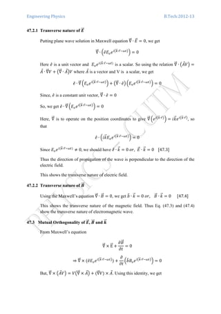
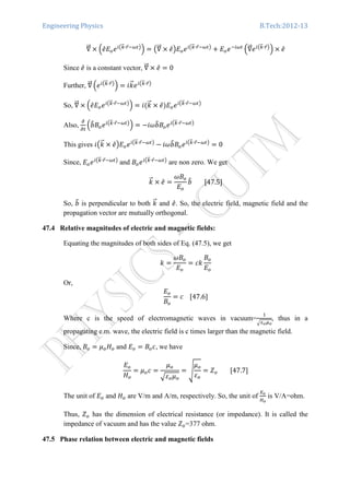
![Engineering Physics B.Tech:2012-13
The electric field and the magnetic field, in the e.m. wave, are in phase. When the
electric field attains the maximum value, the magnetic field also attains the maximum
value. Similarly, they become zero at the same time.
(see 1). However, in a conducting medium, there is a phase .difference between the
electric and magnetic fields.
Since the magnitude and direction of the electric and magnetic fields in e.m. wave are
related, only one of them can be used to describe the e.m. wave. Conventionally, the
electric field is chosen for this purpose, because E is c times larger than B and most of
the instruments used to detect e.m. wave deal with the electric rather than the
magnetic component of the wave. For example, the plane of vibration of the
electromagnetic wave (such as light) is taken as the plane containing the electric field.
[Reference: Physics-I by B.B. swain and P. K. Jena, Pages: 262-266]
48 Electromagnetic energy and Poynting theorem
The electromagnetic waves carry energy and momentum when they propagate. The
conservation of energy in electromagnetic wave phenomena is described by Poynting
theorem.
48.1 Electromagnetic energy density
The electric energy per unit volume is given by
In vacuum, is replaced by
The magnetic energy per unit volume is given by
In vacuum, is replaced by .](https://image.slidesharecdn.com/engineeringphysics-151212062959/85/Engineering-physics-100-320.jpg)
![Engineering Physics B.Tech:2012-13
The electromagnetic energy density is given by
ݑாெ ൌ
1
2
൫ܧሬԦ ∙ ܦሬሬԦ ܤሬԦ ∙ ܪሬሬԦ൯ ൌ
1
2
ሺߝܧଶ
ߤܪଶሻ ሾ48.3ሿ
The total electromagnetic energy in a region is obtained by taking the volume integral
of the e.m. energy density over the total volume under consideration.
48.2 Poynting vector
The rate of energy transport per unit area in electromagnetic wave is described by a
vector called Poynting vector, named after John Henry Poynting (1852-1914). The
Poynting vector ݏԦ for electromagnetic wave is defined in terms of the electric and
magnetic fields by
ܵԦ ൌ ܧሬԦ ൈ ܪሬሬԦ ൌ
ܧሬԦ ൈ ܤሬԦ
ߤ
ሾ48.4ሿ
The Poynting vector measures the flow of electromagnetic energy per unit time per
unit area normal to the direction of wave propagation. Its S.I. unit is watt / (metre)2
,
The direction of Poynting vector is perpendicular to both the electric and magnetic
fields. It is directed along the direction of propagation of the e.m. wave.
48.3Poynting theorem
From Maxwell's curl equations, we have
ሬሬԦ ൈ EሬሬԦ ൌ െ
߲ܤሬԦ
߲ݐ
ሾ1ሿ
ሬሬԦ ൈ ܪሬሬԦ ൌ
߲ܦሬሬԦ
߲ݐ
ܬԦ ሾ2ሿ
Taking the dot product of eq[1] with ܪሬሬԦ, we get
ܪሬሬԦ ∙ ሬሬԦ ൈ EሬሬԦ ൌ െܪሬሬԦ ∙
߲ܤሬԦ
߲ݐ
ሾ3ሿ
Taking the dot product of eq[2] with ܧሬԦ, we get
ܧሬԦ ∙ ሬሬԦ ൈ ܪሬሬԦ ൌ ܧሬԦ ∙
߲ܦሬሬԦ
߲ݐ
ܧሬԦ ∙ ܬԦ ሾ4ሿ
Subtracting eq[4] from eq[3], we get
ܪሬሬԦ ∙ ሬሬԦ ൈ EሬሬԦ െ ܧሬԦ ∙ ሬሬԦ ൈ ܪሬሬԦ ൌ െܪሬሬԦ ∙
߲ܤሬԦ
߲ݐ
െ ܧሬԦ ∙
߲ܦሬሬԦ
߲ݐ
െ ܧሬԦ ∙ ܬԦ ሾ5ሿ](https://image.slidesharecdn.com/engineeringphysics-151212062959/85/Engineering-physics-101-320.jpg)
![Engineering Physics B.Tech:2012-13
We know that, from vector calculus, ሬሬԦ ∙ ൫ܧሬԦ ൈ ܪሬሬԦ൯ ൌ ܪሬሬԦ ∙ ൫ሬሬԦ ൈ ܧሬԦ൯ െ ܧሬԦ ∙ ሺሬሬԦ ൈ ܪሬሬԦሻ
So, L.H. S. of eq[5]= ሬሬԦ ∙ ൫ܧሬԦ ൈ ܪሬሬԦ൯
Now, the R.H.S is simplified below:
ܪሬሬԦ ∙
߲ܤሬԦ
߲ݐ
ൌ ܪሬሬԦ ∙
߲൫ߤܪሬሬԦ൯
߲ݐ
ൌ ߤܪሬሬԦ ∙
߲ܪሬሬԦ
߲ݐ
ൌ
ߤ
2
߲൫ܪሬሬԦ ∙ ܪሬሬԦ൯
߲ݐ
ൌ
߲
߲ݐ
ቆ
ߤܪଶ
2
ቇ
Similarly,
ܧሬԦ ∙
߲ܦሬሬԦ
߲ݐ
ൌ ܧሬԦ ∙
߲൫ߝܧሬԦ൯
߲ݐ
ൌ ߝܧሬԦ ∙
߲ܧሬԦ
߲ݐ
ൌ
ߝ
2
߲൫ܧሬԦ ∙ ܧሬԦ൯
߲ݐ
ൌ
߲
߲ݐ
ቆ
ߝܧଶ
2
ቇ
Substituting these in eq[5] gives
ሬሬԦ ∙ ൫ܧሬԦ ൈ ܪሬሬԦ൯ ൌ െ
߲
߲ݐ
ቆ
ߝܧଶ
2
ߤܪଶ
2
ቇ െ ܧሬԦ ∙ ܬԦ
Using the definitions of electromagnetic energy density and Poynting vector, we can
write this equation as
ሬሬԦ ∙ ܵԦ ൌ െ
߲ݑாெ
߲ݐ
െ ܧሬԦ ∙ ܬԦ ሾ6ሿ
This is sometimes called the differential form of Poynting theorem.
Taking the volume integral of both the sides over a given volume,
න ሬሬԦ ∙ ܵԦ
ܸ݀ ൌ െ න
߲ݑாெ
߲ݐ
ܸ݀
െ න ܧሬԦ ∙ ܬԦ
ܸ݀
Using Gauss divergence theorem, the LHS can be converted to a surface integral over
a closed surface A enclosing the volume V.
So,
ර ܵԦ ∙ ݀ܣԦ
ൌ െ න
߲ݑாெ
߲ݐ
ܸ݀
െ න ܧሬԦ ∙ ܬԦ
ܸ݀ ሾ7ሿ
This represents the Poynting theorem.
The LHS is the rate of flow of total e.m. energy through the closed area enclosing the
given volume. The 1st term on the RHS is the rate of change of e.m. energy in the
volume. The 2nd term on the RHS is the rate of work done by the electric field on the
source of current. According to Poynting theorem, the rate of flow of e.m. energy
through the surface of a given closed area is equal to the sum of (i) the rate of](https://image.slidesharecdn.com/engineeringphysics-151212062959/85/Engineering-physics-102-320.jpg)
![Engineering Physics B.Tech:2012-13
decrease of e.m. energy in the region enclosed by it and (ii) the rate of work done by
the electric field on the source of current present within the enclosed region. Thus
Poynting theorem is a statement of conservation of energy in electromagnetic field.
The Poynting vector plays the role of flux of e.m. field.
In the absence of any source, ଔԦ ൌ 0. So, Eq. (6) becomes
ሬሬԦ ∙ ܵԦ
߲ݑாெ
߲ݐ
ൌ 0
This is called the equation of continuity for e.m. wave.
[Reference: Physics-I by B.B. swain and P. K. Jena, Pages: 266-268]
Session-49
49 Poynting vector and intensity of electromagnetic wave
In e.m. waves, the electric field E and magnetic field B are time varying fields. So, the
Poynting vector is also a time varying quantity. Since the electric and magnetic fields
are mutually perpendicular, the magnitude of Poynting vector, from Eq. (48.4), is
ܵ ൌ ܪܧ ൌ
ܤܧ
ߤ
This equation is in terms of the instantaneous values of the field components and the
Poynting vector. Since the electric and magnetic fields in e.m. wave are in phase, the
ratio of their maximum values is also equal to the ratio of their instantaneous values.
From Eq.(47.7).
ܧ
ܪ
ൌ
ܧ
ܪ
ൌ ߤܿ ܵ ,ݎ ൌ
ܧଶ
ߤܿ
If ܧ ൌ ܧ sin ߱,ݐ the time average value of the Poynting vector is the intensity of the
e.m. wave which is equal to the average e.m. energy flowing per unit time across unit
area normal to the direction of flow.
Intensity ܫ ൌ 〈ܵ〉 ൌ ܿߝܧ௦
ଶ
Or, ܫ ൌ 〈ܵ〉 ൌ ܿݑா
[Reference: Physics-I by B.B. swain and P. K. Jena, Pages: 268-269]](https://image.slidesharecdn.com/engineeringphysics-151212062959/85/Engineering-physics-103-320.jpg)

This document provides lecture notes on engineering physics for an engineering course. It covers topics on atomic structure, electronic configurations, electrical conduction, and electron theories of metals. The document begins with an introduction to atomic structure, including the components of atoms and Madelung's and Hund's rules for electron configuration. It then discusses electrical conduction, defining terms like resistivity, conductivity, and classifications of materials. The remainder of the document covers electron theories of metals, including classical free electron theory, quantum free electron theory, and band theory. Key concepts from each theory are summarized.