Embedded systems ___vlsi_design
•
1 like•921 views

This document provides the course structure and syllabus for the M.Tech program in Embedded Systems & VLSI Design/VLSI and Embedded Systems (R13 Regulations) at Jawaharlal Nehru Technological University Hyderabad. It lists the various subjects to be covered in each semester of the 2-year program, along with their credit hours. In the first year, subjects include Microcontrollers for Embedded System Design, VLSI Technology and Design, CMOS Analog Integrated Circuit Design, CPLD and FPGA Architectures and Applications. Electives offered are Hardware Software Co-Design, Digital System Design, and Soft Computing Techniques. The second year involves a comprehensive viva, project work and seminar

Recommended
More Related Content
What's hot
What's hot (20)
Viewers also liked
Viewers also liked (13)
Similar to Embedded systems ___vlsi_design
Similar to Embedded systems ___vlsi_design (20)
More from sartaj ahmed
Recently uploaded
Recently uploaded (20)
Embedded systems ___vlsi_design
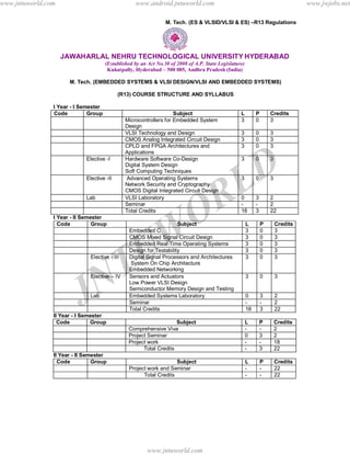
- 1. www.android.jntuworld.com www.jwjobs.net M. Tech. (ES & VLSID/VLSI & ES) –R13 Regulations JAWAHARLAL NEHRU TECHNOLOGICAL UNIVERSITY HYDERABAD (Established by an Act No.30 of 2008 of A.P. State Legislature) Kukatpally, Hyderabad – 500 085, Andhra Pradesh (India) M. Tech. (EMBEDDED SYSTEMS & VLSI DESIGN/VLSI AND EMBEDDED SYSTEMS) (R13) COURSE STRUCTURE AND SYLLABUS I Year - I Semester Code Group Subject L P Credits Microcontrollers for Embedded System Design 3 0 3 VLSI Technology and Design 3 0 3 CMOS Analog Integrated Circuit Design 3 0 3 CPLD and FPGA Architectures and Applications JNTUWORLD 3 0 3 Elective -I Hardware Software Co-Design 3 0 3 Digital System Design Soft Computing Techniques Elective -II Advanced Operating Systems 3 0 3 Network Security and Cryptography CMOS Digital Integrated Circuit Design Lab VLSI Laboratory 0 3 2 Seminar - - 2 Total Credits 18 3 22 I Year - II Semester Code Group Subject L P Credits Embedded C 3 0 3 CMOS Mixed Signal Circuit Design 3 0 3 Embedded Real Time Operating Systems 3 0 3 Design for Testability 3 0 3 Elective - III Digital Signal Processors and Architectures System On Chip Architecture Embedded Networking 3 0 3 Elective – IV Sensors and Actuators Low Power VLSI Design Semiconductor Memory Design and Testing 3 0 3 Lab Embedded Systems Laboratory 0 3 2 Seminar - - 2 Total Credits 18 3 22 II Year - I Semester Code Group Subject L P Credits Comprehensive Viva - - 2 Project Seminar 0 3 2 Project work - - 18 Total Credits - 3 22 II Year - II Semester Code Group Subject L P Credits Project work and Seminar - - 22 Total Credits - - 22 www.jntuworld.com www.jntuworld.com
- 2. www.android.jntuworld.com www.jwjobs.net M. Tech. (ES & VLSID/VLSI & ES) –R13 Regulations JAWAHARLAL NEHRU TECHNOLOGICAL UNIVERSITY HYDERABAD M. Tech – I Year – I Sem. (ES & VLSID/VLSI & ES) MICROCONTROLLERS FOR EMBEDDED SYSTEM DESIGN UNIT –I: ARM Architecture: ARM Design Philosophy, Registers, Program Status Register, Instruction Pipeline, Interrupts and Vector Table, Architecture Revision, ARM Processor Families. UNIT –II: ARM Programming Model – I: Instruction Set: Data Processing Instructions, Addressing Modes, Branch, Load, Store Instructions, PSR Instructions, Conditional Instructions. UNIT –III: ARM Programming Model – II: Thumb Instruction Set: Register Usage, Other Branch Instructions, Data Processing Instructions, Single-Register and Multi Register Load-Store Instructions, Stack, Software Interrupt Instructions UNIT –IV: ARM Programming: Simple C Programs using Function Calls, Pointers, Structures, Integer and Floating Point Arithmetic, Assembly Code using Instruction Scheduling, Register Allocation, Conditional Execution and Loops. UNIT –V: Memory Management: Cache Architecture, Polices, Flushing and Caches, MMU, Page Tables, Translation, Access Permissions, Context Switch. TEXT BOOKS: JNTUWORLD 1. ARM Systems Developer’s Guides- Designing & Optimizing System Software – Andrew N. Sloss, Dominic Symes, Chris Wright, 2008, Elsevier. REFERENCE BOOKS: 2. Embedded Microcomputer Systems, Real Time Interfacing – Jonathan W. Valvano – Brookes / Cole, 1999, Thomas Learning. www.jntuworld.com www.jntuworld.com
- 3. www.android.jntuworld.com www.jwjobs.net M. Tech. (ES & VLSID/VLSI & ES) –R13 Regulations JAWAHARLAL NEHRU TECHNOLOGICAL UNIVERSITY HYDERABAD M. Tech – I Year – I Sem. (ES & VLSID/VLSI & ES) VLSI TECHNOLOGY AND DESIGN UNIT –I: Review of Microelectronics and Introduction to MOS Technologies: MOS, CMOS, BiCMOS Technology. Basic Electrical Properties of MOS, CMOS & BiCMOS Circuits: Ids – Vds relationships, Threshold Voltage VT, Gm, Gds and ωo, Pass Transistor, MOS, CMOS & Bi CMOS Inverters, Zpu/Zpd, MOS Transistor circuit model, Latch-up in CMOS circuits. UNIT –II: Layout Design and Tools: Transistor structures, Wires and Vias, Scalable Design rules, Layout Design tools. Logic Gates & Layouts: Static Complementary Gates, Switch Logic, Alternative Gate circuits, Low power gates, Resistive and Inductive interconnect delays. UNIT –III: Combinational Logic Networks: Layouts, Simulation, Network delay, Interconnect design, Power optimization, Switch logic networks, Gate and Network testing. UNIT –IV: Sequential Systems: Memory cells and Arrays, Clocking disciplines, Design, Power optimization, Design validation and testing. UNIT –V: Floor Planning: Floor planning methods, Global Interconnect, Floor Plan Design, Off-chip connections. TEXT BOOKS: JNTUWORLD 1. Essentials of VLSI Circuits and Systems, K. Eshraghian Eshraghian. D, A. Pucknell, 2005, PHI. 2. Modern VLSI Design – Wayne Wolf, 3rd Ed., 1997, Pearson Education. REFERENCE BOOKS: 1. Introduction to VLSI Systems: A Logic, Circuit and System Perspective – Ming-BO Lin, CRC Press, 2011. 2. Principals of CMOS VLSI Design – N.H.E Weste, K. Eshraghian, 2nd Ed., Addison Wesley. www.jntuworld.com www.jntuworld.com
- 4. www.android.jntuworld.com www.jwjobs.net M. Tech. (ES & VLSID/VLSI & ES) –R13 Regulations JAWAHARLAL NEHRU TECHNOLOGICAL UNIVERSITY HYDERABAD M. Tech – I Year – I Sem. (ES & VLSID/VLSI & ES) CMOS ANALOG INTEGRATED CIRCUIT DESIGN UNIT -I: MOS Devices and Modeling: The MOS Transistor, Passive Components- Capacitor & Resistor, Integrated circuit Layout, CMOS Device Modeling - Simple MOS Large-Signal Model, Other Model Parameters, Small-Signal Model for the MOS Transistor, Computer Simulation Models, Sub-threshold MOS Model. UNIT -II: Analog CMOS Sub-Circuits: MOS Switch, MOS Diode, MOS Active Resistor, Current Sinks and Sources, Current Mirrors-Current mirror with Beta Helper, Degeneration, Cascode current Mirror and Wilson Current Mirror, Current and Voltage References, Band gap Reference. UNIT -III: CMOS Amplifiers: Inverters, Differential Amplifiers, Cascode Amplifiers, Current Amplifiers, Output Amplifiers, High Gain Amplifiers Architectures. UNIT -IV: CMOS Operational Amplifiers: Design of CMOS Op Amps, Compensation of Op Amps, Design of Two-Stage Op Amps, Power- Supply Rejection Ratio of Two-Stage Op Amps, Cascode Op Amps, Measurement Techniques of OP Amp. UNIT -V: Comparators: Characterization of Comparator, Two-Stage, Open-Loop Comparators, Other Open-Loop Comparators, Improving the Performance of Open-Loop Comparators, Discrete-Time Comparators. TEXT BOOKS: JNTUWORLD 1. CMOS Analog Circuit Design - Philip E. Allen and Douglas R. Holberg, Oxford University Press, International Second Edition/Indian Edition, 2010. 2. Analysis and Design of Analog Integrated Circuits- Paul R. Gray, Paul J. Hurst, S. Lewis and R. G. Meyer, Wiley India, Fifth Edition, 2010. REFERENCE BOOKS: 1. Analog Integrated Circuit Design- David A. Johns, Ken Martin, Wiley Student Edn, 2013. 2. Design of Analog CMOS Integrated Circuits- Behzad Razavi, TMH Edition. 3. CMOS: Circuit Design, Layout and Simulation- Baker, Li and Boyce, PHI. www.jntuworld.com www.jntuworld.com
- 5. www.android.jntuworld.com www.jwjobs.net M. Tech. (ES & VLSID/VLSI & ES) –R13 Regulations JAWAHARLAL NEHRU TECHNOLOGICAL UNIVERSITY HYDERABAD M. Tech – I Year – I Sem. (ES & VLSID/VLSI & ES) CPLD AND FPGA ARCHITECURES AND APPLICATIONS UNIT-I: Introduction to Programmable Logic Devices: Introduction, Simple Programmable Logic Devices – Read Only Memories, Programmable Logic Arrays, Programmable Array Logic, Programmable Logic Devices/Generic Array Logic; Complex Programmable Logic Devices – Architecture of Xilinx Cool Runner XCR3064XL CPLD, CPLD Implementation of a Parallel Adder with Accumulation. UNIT-II: Field Programmable Gate Arrays: Organization of FPGAs, FPGA Programming Technologies, Programmable Logic Block Architectures, Programmable Interconnects, Programmable I/O blocks in FPGAs, Dedicated Specialized Components of FPGAs, Applications of FPGAs. UNIT -III: SRAM Programmable FPGAs: Introduction, Programming Technology, Device Architecture, The Xilinx XC2000, XC3000 and XC4000 Architectures. UNIT -IV: Anti-Fuse Programmed FPGAs: Introduction, Programming Technology, Device Architecture, The Actel ACT1, ACT2 and ACT3 Architectures. UNIT -V: Design Applications: General Design Issues, Counter Examples, A Fast Video Controller, A Position Tracker for a Robot Manipulator, A Fast DMA Controller, Designing Counters with ACT devices, Designing Adders and Accumulators with the ACT Architecture. TEXT BOOKS: JNTUWORLD 1. Field Programmable Gate Array Technology - Stephen M. Trimberger, Springer International Edition. 2. Digital Systems Design - Charles H. Roth Jr, Lizy Kurian John, Cengage Learning. REFERENCE BOOKS: 1. Field Programmable Gate Arrays - John V. Oldfield, Richard C. Dorf, Wiley India. 2. Digital Design Using Field Programmable Gate Arrays - Pak K. Chan/Samiha Mourad, Pearson Low Price Edition. 3. Digital Systems Design with FPGAs and CPLDs - Ian Grout, Elsevier, Newnes. 4. FPGA based System Design - Wayne Wolf, Prentice Hall Modern Semiconductor Design Series. www.jntuworld.com www.jntuworld.com
- 6. www.android.jntuworld.com www.jwjobs.net M. Tech. (ES & VLSID/VLSI & ES) –R13 Regulations JAWAHARLAL NEHRU TECHNOLOGICAL UNIVERSITY HYDERABAD M. Tech – I Year – I Sem. (ES & VLSID/VLSI & ES) HARDWARE - SOFTWARE CO-DESIGN (ELECTIVE -I) UNIT –I: Co- Design Issues: Co- Design Models, Architectures, Languages, A Generic Co-design Methodology. Co- Synthesis Algorithms: Hardware software synthesis algorithms: hardware – software partitioning distributed system co-synthesis. UNIT –II: Prototyping and Emulation: Prototyping and emulation techniques, prototyping and emulation environments, future developments in emulation and prototyping architecture specialization techniques, system communication infrastructure Target Architectures: Architecture Specialization techniques, System Communication infrastructure, Target Architecture and Application System classes, Architecture for control dominated systems (8051-Architectures for High performance control), Architecture for Data dominated systems (ADSP21060, TMS320C60), Mixed Systems. UNIT –III: Compilation Techniques and Tools for Embedded Processor Architectures: Modern embedded architectures, embedded software development needs, compilation technologies, practical consideration in a compiler development environment. UNIT –IV: Design Specification and Verification: Design, co-design, the co-design computational model, concurrency coordinating concurrent computations, interfacing components, design verification, implementation verification, verification tools, interface verification UNIT –V: Languages for System – Level Specification and Design-I: System – level specification, design representation for system level synthesis, system level specification languages, Languages for System – Level Specification and Design-II: Heterogeneous specifications and multi language co-simulation, the cosyma system and lycos system. TEXT BOOKS: JNTUWORLD 1. Hardware / Software Co- Design Principles and Practice – Jorgen Staunstrup, Wayne Wolf – 2009, Springer. 2. Hardware / Software Co- Design - Giovanni De Micheli, Mariagiovanna Sami, 2002, Kluwer Academic Publishers REFERENCE BOOKS: 1. A Practical Introduction to Hardware/Software Co-design -Patrick R. Schaumont - 2010 – Springer www.jntuworld.com www.jntuworld.com
- 7. www.android.jntuworld.com www.jwjobs.net M. Tech. (ES & VLSID/VLSI & ES) –R13 Regulations JAWAHARLAL NEHRU TECHNOLOGICAL UNIVERSITY HYDERABAD M. Tech – I Year – I Sem. (ES & VLSID/VLSI & ES) DIGITAL SYSTEM DESIGN (ELECTIVE -I) UNIT -I: Minimization and Transformation of Sequential Machines: The Finite State Model – Capabilities and limitations of FSM – State equivalence and machine minimization – Simplification of incompletely specified machines. Fundamental mode model – Flow table – State reduction – Minimal closed covers – Races, Cycles and Hazards. UNIT -II: Digital Design: Digital Design Using ROMs, PALs and PLAs , BCD Adder, 32 – bit adder, State graphs for control circuits, Scoreboard and Controller, A shift and add multiplier, Array multiplier, Keypad Scanner, Binary divider. UNIT -III: SM Charts: State machine charts, Derivation of SM Charts, Realization of SM Chart, Implementation of Binary Multiplier, dice game controller. UNIT -IV: Fault Modeling & Test Pattern Generation: Logic Fault model – Fault detection & Redundancy- Fault equivalence and fault location –Fault dominance – Single stuck at fault model – Multiple stuck at fault models –Bridging fault model. Fault diagnosis of combinational circuits by conventional methods – Path sensitization techniques, Boolean Difference method – Kohavi algorithm – Test algorithms – D algorithm, PODEM, Random testing, Transition count testing, Signature analysis and test bridging faults. UNIT -V: Fault Diagnosis in Sequential Circuits: Circuit Test Approach, Transition Check Approach – State identification and fault detection experiment, Machine identification, Design of fault detection experiment TEXT BOOKS: JNTUWORLD 1. Fundamentals of Logic Design – Charles H. Roth, 5th Ed., Cengage Learning. 2. Digital Systems Testing and Testable Design – Miron Abramovici, Melvin A. Breuer and Arthur D. Friedman- John Wiley & Sons Inc. 3. Logic Design Theory – N. N. Biswas, PHI REFERENCE BOOKS: 1. Switching and Finite Automata Theory – Z. Kohavi , 2nd Ed., 2001, TMH 2. Digital Design – Morris Mano, M.D.Ciletti, 4th Edition, PHI. 3. Digital Circuits and Logic Design – Samuel C. Lee , PHI www.jntuworld.com www.jntuworld.com
- 8. www.android.jntuworld.com www.jwjobs.net M. Tech. (ES & VLSID/VLSI & ES) –R13 Regulations JAWAHARLAL NEHRU TECHNOLOGICAL UNIVERSITY HYDERABAD M. Tech – I Year – I Sem. (ES & VLSID/VLSI & ES) SOFT COMPUTING TECHNIQUES (ELECTIVE -I) UNIT –I: Introduction: Approaches to intelligent control, Architecture for intelligent control, Symbolic reasoning system, Rule-based systems, the AI approach, Knowledge representation - Expert systems. UNIT –II: Artificial Neural Networks: Concept of Artificial Neural Networks and its basic mathematical model, McCulloch-Pitts neuron model, simple perceptron, Adaline and Madaline, Feed-forward Multilayer Perceptron, Learning and Training the neural network, Data Processing: Scaling, Fourier transformation, principal-component analysis and wavelet transformations, Hopfield network, Self-organizing network and Recurrent network, Neural Network based controller. UNIT –III: Fuzzy Logic System: Introduction to crisp sets and fuzzy sets, basic fuzzy set operation and approximate reasoning, Introduction to fuzzy logic modeling and control, Fuzzification, inferencing and defuzzification, Fuzzy knowledge and rule bases, Fuzzy modeling and control schemes for nonlinear systems, Self-organizing JNTUWORLD fuzzy logic control, Fuzzy logic control for nonlinear time delay system. UNIT –IV: Genetic Algorithm: Basic concept of Genetic algorithm and detail algorithmic steps, Adjustment of free parameters, Solution of typical control problems using genetic algorithm, Concept on some other search techniques like Tabu search and anD-colony search techniques for solving optimization problems. UNIT –V: Applications: GA application to power system optimisation problem, Case studies: Identification and control of linear and nonlinear dynamic systems using MATLAB-Neural Network toolbox, Stability analysis of Neural- Network interconnection systems, Implementation of fuzzy logic controller using MATLAB fuzzy-logic toolbox, Stability analysis of fuzzy control systems. TEXT BOOKS: 1. Introduction to Artificial Neural Systems - Jacek.M.Zurada, Jaico Publishing House, 1999. 2. Neural Networks and Fuzzy Systems - Kosko, B., Prentice-Hall of India Pvt. Ltd., 1994. REFERENCE BOOKS: 1. Fuzzy Sets, Uncertainty and Information - Klir G.J. & Folger T.A., Prentice-Hall of India Pvt. Ltd., 1993. 2. Fuzzy Set Theory and Its Applications - Zimmerman H.J. Kluwer Academic Publishers, 1994. 3. Introduction to Fuzzy Control - Driankov, Hellendroon, Narosa Publishers. 4. Artificial Neural Networks - Dr. B. Yagananarayana, 1999, PHI, New Delhi. 5. Elements of Artificial Neural Networks - Kishan Mehrotra, Chelkuri K. Mohan, Sanjay Ranka, Penram International. 6. Artificial Neural Network –Simon Haykin, 2nd Ed., Pearson Education. 7. Introduction Neural Networks Using MATLAB 6.0 - S.N. Shivanandam, S. Sumati, S. N. Deepa,1/e, TMH, New Delhi. www.jntuworld.com www.jntuworld.com
- 9. www.android.jntuworld.com www.jwjobs.net M. Tech. (ES & VLSID/VLSI & ES) –R13 Regulations JAWAHARLAL NEHRU TECHNOLOGICAL UNIVERSITY HYDERABAD M. Tech – I Year – I Sem. (ES & VLSID/VLSI & ES) ADVANCED OPERATING SYSTEMS (ELECTIVE -II) UNIT –I: Introduction to Operating Systems: Overview of computer system hardware, Instruction execution, I/O function, Interrupts, Memory hierarchy, I/O Communication techniques, Operating system objectives and functions, Evaluation of operating System UNIT –II: Introduction to UNIX and LINUX: Basic Commands & Command Arguments, Standard Input, Output, Input / Output Redirection, Filters and Editors, Shells and Operations UNIT –III: System Calls: System calls and related file structures, Input / Output, Process creation & termination. Inter Process Communication: Introduction, File and record locking, Client – Server example, Pipes, FIFOs, Streams & Messages, Name Spaces, Systems V IPC, Message queues, Semaphores, Shared Memory, Sockets & TLI. UNIT –IV: Introduction to Distributed Systems: Goals of distributed system, Hardware and software concepts, Design issues. Communication in Distributed Systems: Layered protocols, ATM networks, Client - Server model, Remote procedure call and Group communication. UNIT –V: Synchronization in Distributed Systems: Clock synchronization, Mutual exclusion, E-tech algorithms, Bully algorithm, Ring algorithm, Atomic transactions Deadlocks: Dead lock in distributed systems, Distributed dead lock prevention and distributed dead lock detection. TEXT BOOKS: 1. The Design of the UNIX Operating Systems – Maurice J. Bach, 1986, PHI. 2. Distributed Operating System - Andrew. S. Tanenbaum, 1994, PHI. 3. The Complete Reference LINUX – Richard Peterson, 4th Ed., McGraw – Hill. REFERENCE BOOKS: 1. Operating Systems: Internal and Design Principles - Stallings, 6th Ed., PE. 2. Modern Operating Systems - Andrew S Tanenbaum, 3rd Ed., PE. 3. Operating System Principles - Abraham Silberchatz, Peter B. Galvin, Greg Gagne, 7th Ed., JNTUWORLD John Wiley 4. UNIX User Guide – Ritchie & Yates. 5. UNIX Network Programming - W.Richard Stevens, 1998, PHI. www.jntuworld.com www.jntuworld.com
- 10. www.android.jntuworld.com www.jwjobs.net M. Tech. (ES & VLSID/VLSI & ES) –R13 Regulations JAWAHARLAL NEHRU TECHNOLOGICAL UNIVERSITY HYDERABAD M. Tech – I Year – I Sem. (ES & VLSID/VLSI & ES) NETWORK SECURITY AND CRYPTOGRAPHY (ELECTIVE – II) UNIT –I: Introduction: Attacks, Services and Mechanisms, Security attacks, Security services, A Model for Internetwork security.Classical Techniques: Conventional Encryption model, Steganography, Classical Encryption Techniques. UNIT –II: Modern Techniques: Simplified DES, Block Cipher Principles, Data Encryption standard, Strength of DES, Differential and Linear Cryptanalysis, Block Cipher Design Principles and Modes of operations. Algorithms: Triple DES, International Data Encryption algorithm, Blowfish, RC5, CAST-128, RC2, Characteristics of Advanced Symmetric block cifers. Conventional Placement Generation. Public Principles, Cryptography. UNIT Number Prime primality, Message Authentication functions JNTUWORLD Encryption: of Encryption function, Traffic confidentiality, Key distribution, Random Number Key Cryptography: RSA Algorithm, Key Management, Diffie-Hellman Key exchange, Elliptic Curve –III: Theory: and Relatively prime numbers, Modular arithmetic, Fermat’s and Euler’s theorems, Testing for Euclid’s Algorithm, the Chinese remainder theorem, Discrete logarithms. authentication and Hash Functions: requirements and functions, Message Authentication, Hash functions, Security of Hash and MACs. UNIT –IV: Hash and Mac Algorithms: MD File, Message digest Algorithm, Secure Hash Algorithm, RIPEMD-160, HMAC. Digital signatures and Authentication Protocols: Digital signatures, Authentication Protocols, Digital signature standards. Authentication Applications: Kerberos, X.509 directory Authentication service.Electronic Mail Security: Pretty Good Privacy, S/MIME. UNIT –V: IP Security: Overview, Architecture, Authentication, Encapsulating Security Payload, Combining security Associations, Key Management. Web Security: Web Security requirements, Secure sockets layer and Transport layer security, Secure Electronic Transaction. Intruders, Viruses and Worms: Intruders, Viruses and Related threats. Fire Walls: Fire wall Design Principles, Trusted systems. TEXT BOOKS: 1. Cryptography and Network Security: Principles and Practice - William Stallings, 2000, PE. REFERENCES: 1. Principles of Network and Systems Administration, Mark Burgess,John Wiel www.jntuworld.com www.jntuworld.com
- 11. www.android.jntuworld.com www.jwjobs.net M. Tech. (ES & VLSID/VLSI & ES) –R13 Regulations JAWAHARLAL NEHRU TECHNOLOGICAL UNIVERSITY HYDERABAD M. Tech – I Year – I Sem. (ES & VLSID/VLSI & ES) CMOS DIGITAL INTEGRATED CIRCUIT DESIGN (ELECTIVE – II) UNIT –I: MOS Design: Pseudo NMOS Logic – Inverter, Inverter threshold voltage, Output high voltage, Output Low voltage, Gain at gate threshold voltage, Transient response, Rise time, Fall time, Pseudo NMOS logic gates, Transistor equivalency, CMOS Inverter logic. UNIT –II: Combinational MOS Logic Circuits: MOS logic circuits with NMOS loads, Primitive CMOS logic gates – NOR & NAND gate, Complex Logic circuits design – Realizing Boolean expressions using NMOS gates and CMOS gates , AOI and OIA gates, CMOS full adder, CMOS transmission gates, Designing with Transmission gates. UNIT –III: Sequential MOS Logic Circuits: Behavior of bistable elements, SR Latch, Clocked latch and flip flop circuits, CMOS D latch and edge triggered flipflop. UNIT –IV: Dynamic Logic Circuits: Basic principle, Voltage Bootstrapping, Synchronous dynamic pass transistor circuits, Dynamic CMOS transmission gate logic, High performance Dynamic CMOS circuits. UNIT –V: Semiconductor Memories: Types, RAM array organization, DRAM – Types, Operation, Leakage currents in DRAM cell and refresh operation, SRAM operation Leakage currents in SRAM cells, Flash Memory- NOR flash and NAND flash. TEXT BOOKS: JNTUWORLD 1. Digital Integrated Circuit Design – Ken Martin, Oxford University Press, 2011. 2. CMOS Digital Integrated Circuits Analysis and Design – Sung-Mo Kang, Yusuf Leblebici, TMH, 3rd Ed., 2011. REFERENCE BOOKS: 1. Introduction to VLSI Systems: A Logic, Circuit and System Perspective – Ming-BO Lin, CRC Press, 2011 2. Digital Integrated Circuits – A Design Perspective, Jan M. Rabaey, Anantha Chandrakasan, Borivoje Nikolic, 2nd Ed., PHI. www.jntuworld.com www.jntuworld.com
- 12. www.android.jntuworld.com www.jwjobs.net M. Tech. (ES & VLSID/VLSI & ES) –R13 Regulations JAWAHARLAL NEHRU TECHNOLOGICAL UNIVERSITY HYDERABAD www.jntuworld.com M. Tech – I Year – I Sem. (ES & VLSID/VLSI & ES) VLSI LABORATORY Note: Minimum of 10 programs from Part –I and 2 programs from Part -II are to be conducted. Design and implementation of the following CMOS digital/analog circuits using Cadence / Mentor Graphics / Synopsys / Equivalent CAD tools. The design shall include Gate-level design, Transistor-level design, Hierarchical design, Verilog HDL/VHDL design, Logic synthesis, Simulation and verification. Part –I: VLSI Front End Design programs: Programming can be done using any complier. Down load the programs on FPGA/CPLD boards and performance testing may be done using pattern generator (32 channels) and logic analyzer apart from verification by simulation with any of the front end tools. 1. HDL code to realize all the logic gates 2. Design and Simulation of adder, Serial Binary Adder, Multi Precession Adder, Carry JNTUWORLD Look Ahead Adder. 3. Design of 2-to-4 decoder 4. Design of 8-to-3 encoder (without and with parity) 5. Design of 8-to-1 multiplexer 6. Design of 4 bit binary to gray converter 7. Design of Multiplexer/ Demultiplexer, comparator 8. Design of Full adder using 3 modeling styles 9. Design of flip flops: SR, D, JK, T 10. Design of 4-bit binary, BCD counters ( synchronous/ asynchronous reset) or any sequence counter 11. Design of a N- bit Register of Serial- in Serial –out, Serial in parallel out, Parallel in Serial out and Parallel in Parallel Out. 12. Design of Sequence Detector (Finite State Machine- Mealy and Moore Machines). 13. Design of 4- Bit Multiplier, Divider. 14. Design of ALU to Perform – ADD, SUB, AND-OR, 1’s and 2’s Compliment, Multiplication, and Division. 15. Design of Finite State Machine. 16. Implementing the above designs on Xilinx/Altera/Cypress/equivalent based FPGA/CPLD kits . Part –II: VLSI Back End Design programs: Design and implementation of the following CMOS digital/analog circuits using Cadence / Mentor Graphics / Synopsys / Equivalent CAD tools. The design shall include Gate-level design/Transistor-level design/Hierarchical design/Verilog HDL or VHDL design, Logic synthesis, Simulation and verification, Scaling of CMOS Inverter for different technologies, study of secondary effects (temperature, power supply and process corners), Circuit optimization with respect to area, performance and/or power, Layout, Extraction of parasitics and back annotation, modifications in circuit parameters and layout consumption, DC/transient analysis, Verification of layouts (DRC, LVS). 1. Introduction to layout design rules 2. Layout, physical verification, placement & route for complex design, static timing analysis, IR drop analysis and crosstalk analysis of the following: Basic logic gates CMOS inverter CMOS NOR/ NAND gates CMOS XOR and MUX gates CMOS 1-bit full adder Static / Dynamic logic circuit (register cell) Latch Pass transistor 3. Layout of any combinational circuit (complex CMOS logic gate)- Learning about data paths www.jntuworld.com
- 13. www.android.jntuworld.com www.jwjobs.net M. Tech. (ES & VLSID/VLSI & ES) –R13 Regulations JAWAHARLAL NEHRU TECHNOLOGICAL UNIVERSITY HYDERABAD M. Tech – I Year – II Sem. (ES & VLSID/VLSI & ES) EMBEDDED C UNIT – I: Programming Embedded Systems in C Introduction ,What is an embedded system, Which processor should you use, Which programming language should you use, Which operating system should you use, How do you develop embedded software, Conclusions Introducing the 8051 Microcontroller Family Introduction, What’s in a name, The external interface of the Standard 8051, Reset requirements ,Clock frequency and performance, Memory issues, I/O pins, Timers, Interrupts, Serial interface, Power consumption ,Conclusions UNIT – II: Reading Switches Introduction, Basic techniques for reading from port pins, Example: Reading and writing bytes, Example: Reading and writing bits (simple version), Example: Reading and writing bits (generic version), The need for pull-up resistors, Dealing with switch bounce, Example: Reading switch inputs (basic code), Example: Counting goats, Conclusions UNIT – III: Adding Structure to the Code Introduction, Object-oriented programming with C, The Project Header (MAIN.H), The Port Header (PORT.H), Example: Restructuring the ‘Hello Embedded World’ example, Example: Restructuring the goat-counting example, Further examples, Conclusions UNIT – IV: Meeting Real-Time Constraints Introduction, Creating ‘hardware delays’ using Timer 0 and Timer 1, Example: Generating a precise 50 ms delay, Example: Creating a portable hardware delay, Why not use Timer 2?, The need for ‘timeout’ mechanisms, Creating loop timeouts, Example: Testing loop timeouts, Example: A more reliable switch interface, Creating hardware timeouts, Example: Testing a hardware timeout, Conclusions UNIT – V: Case Study: Intruder Alarm System Introduction, The software architecture, Key software components used in this example, running the program, the software, Conclusions TEXT BOOKS: JNTUWORLD 1. Embedded C by Michael J. Pont , A Pearson Education REFERENCE BOOKS: 1. PICmicro MCU C-An introduction to programming, The Microchip PIC in CCS C By Nigel Gardner www.jntuworld.com www.jntuworld.com
- 14. www.android.jntuworld.com www.jwjobs.net M. Tech. (ES & VLSID/VLSI & ES) –R13 Regulations JAWAHARLAL NEHRU TECHNOLOGICAL UNIVERSITY HYDERABAD M. Tech – I Year – II Sem. (ES & VLSID/VLSI & ES) CMOS MIXED SIGNAL CIRCUIT DESIGN UNIT -I: Switched Capacitor Circuits: Introduction to Switched Capacitor circuits- basic building blocks, Operation and Analysis, Non-ideal effects in switched capacitor circuits, Switched capacitor integrators first order filters, Switch sharing, biquad filters. UNIT -II: Phased Lock Loop (PLL): Basic PLL topology, Dynamics of simple PLL, Charge pump PLLs-Lock acquisition, Phase/Frequency detector and charge pump, Basic charge pump PLL, Non-ideal effects in PLLs-PFD/CP non-idealities, Jitter in PLLs, Delay locked loops, applications UNIT -III: Data Converter Fundamentals: DC and dynamic specifications, Quantization noise, Nyquist rate D/A converters- Decoder based converters, Binary-Scaled converters, Thermometer-code converters, Hybrid converters UNIT -IV: Nyquist Rate A/D Converters: Successive approximation converters, Flash converter, Two-step A/D converters, Interpolating A/D converters, Folding A/D converters, Pipelined A/D converters, Time-interleaved converters. UNIT -V: Oversampling Converters: Noise shaping modulators, Decimating filters and interpolating filters, Higher order modulators, Delta sigma modulators with multibit quantizers, Delta sigma D/A TEXT BOOKS: 1. Design of Analog CMOS Integrated Circuits- Behzad Razavi, TMH Edition, 2002 2. CMOS Analog Circuit Design - Philip E. Allen and Douglas R. Holberg, Oxford University Press, JNTUWORLD International Second Edition/Indian Edition, 2010. 3. Analog Integrated Circuit Design- David A. Johns,Ken Martin, Wiley Student Edition, 2013 REFERENCE BOOKS: 1. CMOS Integrated Analog-to- Digital and Digital-to-Analog converters-Rudy Van De Plassche, Kluwer Academic Publishers, 2003 2. Understanding Delta-Sigma Data converters-Richard Schreier, Wiley Interscience, 2005. 3. CMOS Mixed-Signal Circuit Design - R. Jacob Baker, Wiley Interscience, 2009. www.jntuworld.com www.jntuworld.com
- 15. www.android.jntuworld.com www.jwjobs.net M. Tech. (ES & VLSID/VLSI & ES) –R13 Regulations JAWAHARLAL NEHRU TECHNOLOGICAL UNIVERSITY HYDERABAD M. Tech – I Year – II Sem. (ES & VLSID/VLSI & ES) EMBEDDED REAL TIME OPERATING SYSTEMS UNIT – I: Introduction Introduction to UNIX/LINUX, Overview of Commands, File I/O,( open, create, close, lseek, read, write), Process Control ( fork, vfork, exit, wait, waitpid, exec. UNIT - II: Real Time Operating Systems Brief History of OS, Defining RTOS, The Scheduler, Objects, Services, Characteristics of RTOS, Defining a Task, asks States and Scheduling, Task Operations, Structure, Synchronization, Communication and Concurrency. Defining Semaphores, Operations and Use, Defining Message Queue, States, Content, Storage, Operations and Use UNIT - III: Objects, Services and I/O Pipes, Event Registers, Signals, Other Building Blocks, Component Configuration, Basic I/O Concepts, I/O Subsystem UNIT - IV: Exceptions, Interrupts and Timers Exceptions, Interrupts, Applications, Processing of Exceptions and Spurious Interrupts, Real Time Clocks, Programmable Timers, Timer Interrupt Service Routines (ISR), Soft Timers, Operations. UNIT - V: Case Studies of RTOS RT Linux, MicroC/OS-II, Vx Works, Embedded Linux, Tiny OS, and Basic Concepts of Android OS. JNTUWORLD TEXT BOOKS: 1. Real Time Concepts for Embedded Systems – Qing Li, Elsevier, 2011 REFERENCE BOOKS: 1. Embedded Systems- Architecture, Programming and Design by Rajkamal, 2007, TMH. 2. Advanced UNIX Programming, Richard Stevens 3. Embedded Linux: Hardware, Software and Interfacing – Dr. Craig Hollabaugh www.jntuworld.com www.jntuworld.com
- 16. www.android.jntuworld.com www.jwjobs.net M. Tech. (ES & VLSID/VLSI & ES) –R13 Regulations JAWAHARLAL NEHRU TECHNOLOGICAL UNIVERSITY HYDERABAD M. Tech – I Year – II Sem. (ES & VLSID/VLSI & ES) DESIGN FOR TESTABILITY UNIT -I: Introduction to Testing: Testing Philosophy, Role of Testing, Digital and Analog VLSI Testing, VLSI Technology Trends affecting Testing, Types of Testing, Fault Modeling: Defects, Errors and Faults, Functional Versus Structural Testing, Levels of Fault Models, Single Stuck-at Fault. UNIT -II: Logic and Fault Simulation: Simulation for Design Verification and Test Evaluation, Modeling Circuits for Simulation, Algorithms for True-value Simulation, Algorithms for Fault Simulation, ATPG. UNIT -III: Testability Measures: SCOAP Controllability and Observability, High Level Testability Measures, Digital DFT and Scan Design: Ad-Hoc DFT Methods, Scan Design, Partial-Scan Design, Variations of Scan. UNIT -IV: Built-In Self-Test: The Economic Case for BIST, Random Logic BIST: Definitions, BIST Process, Pattern Generation, Response Compaction, Built-In Logic Block Observers, Test-Per-Clock, Test-Per-Scan BIST Systems, Circular Self Test Path System, Memory BIST, Delay Fault BIST. UNIT -V: Boundary Scan Standard: Motivation, System Configuration with Boundary Scan: TAP Controller and Port, Boundary Scan Test Instructions, Pin Constraints of the Standard, Boundary Scan Description Language: BDSL Description Components, Pin Descriptions. TEXT BOOKS: JNTUWORLD 1. Essentials of Electronic Testing for Digital, Memory and Mixed Signal VLSI Circuits - M.L. Bushnell, V. D. Agrawal, Kluwer Academic Pulishers. REFERENCE BOOKS: 1. Digital Systems and Testable Design - M. Abramovici, M.A.Breuer and A.D Friedman, Jaico Publishing House. 2. Digital Circuits Testing and Testability - P.K. Lala, Academic Press. www.jntuworld.com www.jntuworld.com
- 17. www.android.jntuworld.com www.jwjobs.net M. Tech. (ES & VLSID/VLSI & ES) –R13 Regulations JAWAHARLAL NEHRU TECHNOLOGICAL UNIVERSITY HYDERABAD M. Tech – I Year – II Sem. (ES & VLSID/VLSI & ES) DIGITAL SIGNAL PROCESSORS AND ARCHITECTURES (ELECTIVE -III) UNIT –I: Introduction to Digital Signal Processing: Introduction, A Digital signal-processing system, The sampling process, Discrete time sequences. Discrete Fourier Transform (DFT) and Fast Fourier Transform (FFT), Linear time-invariant systems, Digital filters, Decimation and interpolation. Computational Accuracy in DSP Implementations: Number formats for signals and coefficients in DSP systems, Dynamic Range and Precision, Sources of error in DSP implementations, A/D Conversion errors, DSP Computational errors, D/A Conversion Errors, Compensating filter. UNIT –II: Architectures for Programmable DSP Devices: Basic Architectural features, DSP Computational Building Blocks, Bus Architecture and Memory, Data Addressing Capabilities, Address Generation UNIT, Programmability and Program Execution, Speed Issues, Features for External interfacing. UNIT -III: Programmable Digital Signal Processors: Commercial Digital signal-processing Devices, Data Addressing modes of TMS320C54XX DSPs, Data Addressing modes of TMS320C54XX Processors, Memory space of TMS320C54XX Processors, Program Control, TMS320C54XX instructions and Programming, On-Chip Peripherals, Interrupts of TMS320C54XX processors, Pipeline Operation of TMS320C54XX Processors. UNIT –IV: Analog Devices Family of DSP Devices: Analog Devices Family of DSP Devices – ALU and MAC block diagram, Shifter Instruction, Base Architecture of ADSP 2100, ADSP-2181 high performance Processor. Introduction to Blackfin Processor - The Blackfin Processor, Introduction to Micro Signal Architecture, Overview of Hardware Processing Units and Register files, Address Arithmetic Unit, Control Unit, Bus Architecture and Memory, Basic Peripherals. UNIT –V: Interfacing Memory and I/O Peripherals to Programmable DSP Devices: Memory space organization, External bus interfacing signals, Memory interface, Parallel I/O interface, Programmed I/O, Interrupts and I/O, Direct memory access (DMA). TEXT BOOKS: 1. Digital Signal Processing – Avtar Singh and S. Srinivasan, Thomson Publications, 2004. 2. A Practical Approach To Digital Signal Processing - K Padmanabhan, R. Vijayarajeswaran, JNTUWORLD Ananthi. S, New Age International, 2006/2009 3. Embedded Signal Processing with the Micro Signal Architecture Publisher: Woon-Seng Gan, Sen M. Kuo, Wiley-IEEE Press, 2007 REFERENCE BOOKS: 1. Digital Signal Processors, Architecture, Programming and Applications – B. Venkataramani and M. Bhaskar, 2002, TMH. 2. Digital Signal Processing – Jonatham Stein, 2005, John Wiley. 3. DSP Processor Fundamentals, Architectures & Features – Lapsley et al. 2000, S. Chand & Co. 4. Digital Signal Processing Applications Using the ADSP-2100 Family by The Applications Engineering Staff of Analog Devices, DSP Division, Edited by Amy Mar, PHI 5. The Scientist and Engineer's Guide to Digital Signal Processing by Steven W. Smith, Ph.D., California Technical Publishing, ISBN 0-9660176-3-3, 1997 6. Embedded Media Processing by David J. Katz and Rick Gentile of Analog Devices, Newnes , ISBN 0750679123, 2005 www.jntuworld.com www.jntuworld.com
- 18. www.android.jntuworld.com www.jwjobs.net M. Tech. (ES & VLSID/VLSI & ES) –R13 Regulations JAWAHARLAL NEHRU TECHNOLOGICAL UNIVERSITY HYDERABAD M. Tech – I Year – II Sem. (ES & VLSID/VLSI & ES) SYSTEM ON CHIP ARCHITECTURE (ELECTIVE -III) UNIT –I: Introduction to the System Approach: System Architecture, Components of the system, Hardware & Software, Processor Architectures, Memory and Addressing. System level interconnection, An approach for SOC Design, System Architecture and Complexity. UNIT –II: Processors: Introduction , Processor Selection for SOC, Basic concepts in Processor Architecture, Basic concepts in Processor Micro Architecture, Basic elements in Instruction handling. Buffers: minimizing Pipeline Delays, Branches, More Robust Processors, Vector Processors and Vector Instructions extensions, VLIW Processors, Superscalar Processors. UNIT –III: Memory Design for SOC: Overview of SOC external memory, Internal Memory, Size, Scratchpads and Cache memory, Cache Organization, Cache data, Write Policies, Strategies for line replacement at miss time, Types of Cache, Split – I, and D – Caches, Multilevel Caches, Virtual to real translation , SOC Memory System, Models of Simple Processor – memory interaction. UNIT -IV: Interconnect Customization and Configuration: Inter Connect Architectures, Bus: Basic Architectures, SOC Standard Buses , Analytic Bus Models, Using the Bus model, Effects of Bus transactions and contention time. SOC Customization: An overview, Customizing Instruction Processor, Reconfiguration Technologies, Mapping design onto Reconfigurable devices, Instance- Specific design, Customizable Soft Processor, Reconfiguration - overhead analysis and trade-off analysis on reconfigurable Parallelism. UNIT –V: Application Studies / Case Studies: SOC Design approach, AES algorithms, Design and evaluation, Image compression – JPEG compression. TEXT BOOKS: JNTUWORLD 1. Computer System Design System-on-Chip - Michael J. Flynn and Wayne Luk, Wiely India Pvt. Ltd. 2. ARM System on Chip Architecture – Steve Furber –2nd Ed., 2000, Addison Wesley Professional. REFERENCE BOOKS: 1. Design of System on a Chip: Devices and Components – Ricardo Reis, 1st Ed., 2004, Springer 2. Co-Verification of Hardware and Software for ARM System on Chip Design (Embedded Technology) – Jason Andrews – Newnes, BK and CDROM. System on Chip Verification – Methodologies and Techniques –Prakash Rashinkar, Peter Paterson and Leena Singh L, 2001, Kluwer Academic Publishers. www.jntuworld.com www.jntuworld.com
- 19. www.android.jntuworld.com www.jwjobs.net M. Tech. (ES & VLSID/VLSI & ES) –R13 Regulations JAWAHARLAL NEHRU TECHNOLOGICAL UNIVERSITY HYDERABAD M. Tech – I Year – II Sem. (ES & VLSID/VLSI & ES) EMBEDDED NETWORKING (ELECTIVE -III) UNIT –I: Embedded Communication Protocols: Embedded Networking: Introduction – Serial/Parallel Communication – Serial communication protocols -RS232 standard – RS485 – Synchronous Serial Protocols -Serial Peripheral Interface (SPI) – Inter Integrated Circuits (I2C) – PC Parallel port programming - ISA/PCI Bus protocols – Firewire. UNIT –II: USB and CAN Bus: USB bus – Introduction – Speed Identification on the bus – USB States – USB bus communication: Packets –Data flow types –Enumeration –Descriptors –PIC 18 Microcontroller USB Interface – C Programs –CAN Bus – Introduction - Frames –Bit stuffing –Types of errors –Nominal Bit Timing – PIC microcontroller CAN Interface –A simple application with CAN. UNIT –III: Ethernet Basics: Elements of a network – Inside Ethernet – Building a Network: Hardware options – Cables, Connections and network speed – Design choices: Selecting components –Ethernet Controllers – Using the internet in local and internet communications – Inside the Internet protocol. UNIT –IV: Embedded Ethernet: Exchanging messages using UDP and TCP – Serving web pages with Dynamic Data – Serving web pages that respond to user Input – Email for Embedded Systems – Using FTP – Keeping Devices and Network secure. UNIT –V: Wireless Embedded Networking: Wireless sensor networks – Introduction – Applications – Network Topology – Localization –Time Synchronization - Energy efficient MAC protocols –SMAC – Energy efficient and robust routing – Data Centric routing. TEXT BOOKS: JNTUWORLD 1. Embedded Systems Design: A Unified Hardware/Software Introduction - Frank Vahid, Tony Givargis, John & Wiley Publications, 2002 2. Parallel Port Complete: Programming, interfacing and using the PCs parallel printer port - Jan Axelson, Penram Publications, 1996. REFERENCE BOOKS: 1. Advanced PIC microcontroller projects in C: from USB to RTOS with the PIC18F series - Dogan Ibrahim, Elsevier 2008. 2. Embedded Ethernet and Internet Complete - Jan Axelson, Penram publications, 2003. 3. Networking Wireless Sensors - Bhaskar Krishnamachari, Cambridge press 2005. www.jntuworld.com www.jntuworld.com
- 20. www.android.jntuworld.com www.jwjobs.net M. Tech. (ES VLSID/VLSI ES) –R13 Regulations JAWAHARLAL NEHRU TECHNOLOGICAL UNIVERSITY HYDERABAD M. Tech – I Year – II Sem. (ES VLSID/VLSI ES) SENSORS AND ACTUATORS (ELECTIVE –IV) UNIT -I: Sensors / Transducers: Principles – Classification – Parameters – Characteristics - Environmental Parameters (EP) – Characterization Mechanical and Electromechanical Sensors: Introduction – Resistive Potentiometer – Strain Gauge – Resistance Strain Gauge – Semiconductor Strain Gauges -Inductive Sensors: Sensitivity and Linearity of the Sensor –Types-Capacitive Sensors:– Electrostatic Transducer– Force/Stress Sensors Using Quartz Resonators – Ultrasonic Sensors UNIT –II: Thermal Sensors: Introduction – Gas thermometric Sensors – Thermal Expansion Type Thermometric Sensors – Acoustic Temperature Sensor – Dielectric Constant and Refractive Index thermosensors – Helium Low Temperature Thermometer – Nuclear Thermometer – Magnetic Thermometer – Resistance Change Type Thermometric Sensors –Thermoemf Sensors– Junction Semiconductor Thermometry Magnetic Anisotropic Inductance Synchro-Sensors UNIT Radiation detectors– Electro Hydrogen Polarization-– JNTUWORLD Types– Thermal Radiation Sensors –Quartz Crystal Thermoelectric Sensors – NQR – Spectroscopic Thermometry – Noise Thermometry – Heat Flux Sensors sensors: Introduction – Sensors and the Principles Behind – Magneto-resistive Sensors – Magnetoresistive Sensing – Semiconductor Magnetoresistors– Hall Effect and Sensors – and Eddy Current Sensors– Angular/Rotary Movement Transducers – Synchros – resolvers - Eddy Current Sensors – Electromagnetic Flowmeter – Switching Magnetic SQUID Sensors -III: Sensors: Introduction – Basic Characteristics – Types of Photosensistors/Photo X-ray and Nuclear Radiation Sensors– Fiber Optic Sensors analytical Sensors: Introduction – The Electrochemical Cell – The Cell Potential - Standard Electrode (SHE) – Liquid Junction and Other Potentials – Polarization – Concentration Reference Electrodes - Sensor Electrodes – Electro ceramics in Gas Media . UNIT -IV: Smart Sensors: Introduction – Primary Sensors – Excitation – Amplification – Filters – Converters – Compensation– Information Coding/Processing - Data Communication – Standards for Smart Sensor Interface – The Automation Sensors –Applications: Introduction – On-board Automobile Sensors (Automotive Sensors)– Home Appliance Sensors – Aerospace Sensors –– Sensors for Manufacturing –Sensors for environmental Monitoring UNIT -V: Actuators: Pneumatic and Hydraulic Actuation Systems- Actuation systems – Pneumatic and hydraulic systems - Directional Control valves – Presure control valves – Cylinders - Servo and proportional control valves – Process control valves – Rotary actuators Mechanical Actuation Systems- Types of motion – Kinematic chains – Cams – Gears – Ratchet and pawl – Belt and chain drives – Bearings – Mechanical aspects of motor selection Electrical Actuation Systems-Electrical systems -Mechanical switches – Solid-state switches Solenoids – D.C. Motors – A.C. motors – Stepper motors TEXT BOOKS: 1. D. Patranabis – “Sensors and Transducers” –PHI Learning Private Limited. 2. W. Bolton – “Mechatronics” –Pearson Education Limited. REFERENCE BOOKS: 1. Sensors and Actuators – D. Patranabis – 2nd Ed., PHI, 2013. www.jntuworld.com www.jntuworld.com
- 21. www.android.jntuworld.com www.jwjobs.net M. Tech. (ES VLSID/VLSI ES) –R13 Regulations JAWAHARLAL NEHRU TECHNOLOGICAL UNIVERSITY HYDERABAD M. Tech – I Year – II Sem. (ES VLSID/VLSI ES) LOW POWER VLSI DESIGN (ELECTIVE -IV) UNIT –I: Fundamentals: Need for Low Power Circuit Design, Sources of Power Dissipation – Switching Power Dissipation, Short Circuit Power Dissipation, Leakage Power Dissipation, Glitching Power Dissipation, Short Channel Effects –Drain Induced Barrier Lowering and Punch Through, Surface Scattering, Velocity Saturation, Impact Ionization, Hot Electron Effect. UNIT –II: Low-Power Design Approaches: Low-Power Design through Voltage Scaling – VTCMOS circuits, MTCMOS circuits, Architectural Level Approach –Pipelining and Parallel Processing Approaches. Switched Capacitance Minimization Approaches: System Level Measures, Circuit Level Measures, Mask level Measures. UNIT –III: Low-Voltage Low-Power Adders: Introduction, Standard Adder Cells, CMOS Adder’s Architectures – Ripple Carry Adders, Carry Look- Ahead Adders, Carry Select Adders, Carry Save Adders, Low-Voltage Low-Power Design Techniques –Trends of Technology and Power Supply Voltage, Low-Voltage Low-Power Logic Styles. UNIT –IV: Low-Voltage Low-Power Multipliers: Introduction, Overview of Multiplication, Types of Multiplier Architectures, Braun Multiplier, Baugh- Wooley Multiplier, Booth Multiplier, Introduction to Wallace Tree Multiplier. UNIT –V: Low-Voltage Low-Power Memories: Basics of ROM, Low-Power ROM Technology, Future Trend and Development of ROMs, Basics of SRAM, Memory Cell, Precharge and Equalization Circuit, Low-Power SRAM Technologies, Basics of DRAM, Self-Refresh Circuit, Future Trend and Development of DRAM. TEXT BOOKS: JNTUWORLD 1. CMOS Digital Integrated Circuits – Analysis and Design – Sung-Mo Kang, Yusuf Leblebici, TMH, 2011. 2. Low-Voltage, Low-Power VLSI Subsystems – Kiat-Seng Yeo, Kaushik Roy, TMH Professional Engineering. REFERENCE BOOKS: 1. Introduction to VLSI Systems: A Logic, Circuit and System Perspective – Ming-BO Lin, CRC Press, 2011 2. Low Power CMOS Design – AnanthaChandrakasan, IEEE Press/Wiley International, 1998. 3. Low Power CMOS VLSI Circuit Design – Kaushik Roy, Sharat C. Prasad, John Wiley Sons, 2000. 4. Practical Low Power Digital VLSI Design – Gary K. Yeap, Kluwer Academic Press, 2002. 5. Low Power CMOS VLSI Circuit Design – A. Bellamour, M. I. Elamasri, Kluwer Academic Press, 1995. 6. Leakage in Nanometer CMOS Technologies – Siva G. Narendran, AnathaChandrakasan, Springer, 2005. www.jntuworld.com www.jntuworld.com
- 22. www.android.jntuworld.com www.jwjobs.net M. Tech. (ES VLSID/VLSI ES) –R13 Regulations JAWAHARLAL NEHRU TECHNOLOGICAL UNIVERSITY HYDERABAD M. Tech – I Year – II Sem. (ES VLSID/VLSI ES) SEMICONDUCTOR MEMORY DESIGN AND TESTING (ELECTIVE -IV) UNIT -I: Random Access Memory Technologies: SRAM – SRAM Cell structures, MOS SRAM Architecture, MOS SRAM cell and peripheral circuit operation, Bipolar SRAM technologies, SOI technology, Advanced SRAM architectures and technologies, Application specific SRAMs, DRAM – DRAM technology development, CMOS DRAM, DRAM cell theory and advanced cell structures, BICMOS DRAM, soft error failure in DRAM, Advanced DRAM design and architecture, Application specific DRAM UNIT -II: Non-volatile Memories: Masked ROMs, High density ROM, PROM, Bipolar ROM, CMOS PROMS, EPROM, Floating gate EPROM cell, One time programmable EPROM, EEPROM, EEPROM technology and architecture, Non-volatile SRAM, Flash Memories (EPROM or EEPROM), advanced Flash memory architecture UNIT -III: Memory Fault Modeling Testing and Memory Design for Testability and Fault Tolerance: RAM fault modeling, Electrical testing, Pseudo Random testing, Megabit DRAM Testing, non-volatile memory modeling and testing, IDDQ fault modeling and testing, Application specific memory testing, RAM fault modeling, BIST techniques for memory UNIT -IV: Semiconductor Memory Reliability and Radiation Effects: General reliability issues RAM failure modes and mechanism, Non-volatile memory reliability, reliability modeling and failure rate prediction, Design for Reliability, Reliability Test Structures, Reliability Screening and qualification, Radiation effects, Single Event Phenomenon (SEP), Radiation Hardening techniques, Radiation Hardening Process and Design Issues, Radiation Hardened Memory characteristics, Radiation Hardness Assurance and Testing, Radiation Dosimetry, Water Level Radiation Testing and Test structures UNIT -V: Advanced Memory Technologies and High-density Memory Packing Technologies: Ferroelectric RAMs (FRAMs), GaAs FRAMs, Analog memories, magneto resistive RAMs (MRAMs), Experimental memory devices, Memory Hybrids and MCMs (2D), Memory Stacks and MCMs (3D), Memory MCM testing and reliability issues, Memory cards, High Density Memory Packaging Future Directions TEXT BOOKS: JNTUWORLD 1. Semiconductor Memories Technology – Ashok K. Sharma, 2002, Wiley. 2. Advanced Semiconductor Memories – Architecture, Design and Applications - Ashok K. Sharma- 2002, Wiley. 3. Modern Semiconductor Devices for Integrated Circuits – Chenming C Hu, 1st Ed., Prentice Hall. www.jntuworld.com www.jntuworld.com
- 23. www.android.jntuworld.com www.jwjobs.net M. Tech. (ES VLSID/VLSI ES) –R13 Regulations JAWAHARLAL NEHRU TECHNOLOGICAL UNIVERSITY HYDERABAD M. Tech – I Year – II Sem. (ES VLSID/VLSI ES) EMBEDDED SYSTEMS LABORATORY Note: The following programs are to be implemented on ARM based Processors/Equivalent. Minimum of 10 programs from Part –I and 6 programs from Part -II are to be conducted. Part -I: The following Programs are to be implemented on ARM Processor 1. Simple Assembly Program for a. Addition | Subtraction | Multiplication | Division b. Operating Modes, System Calls and Interrupts c. Loops, Branches 2. Write an Assembly programs to configure and control General Purpose Input/Output (GPIO) port pins. 3. Write an Assembly programs to read digital values from external peripherals and execute JNTUWORLD them with the Target board. 4. Program for reading and writing of a file 5. Program to demonstrate Time delay program using built in Timer / Counter feature on IDE environment 6. Program to demonstrates a simple interrupt handler and setting up a timer 7. Program demonstrates setting up interrupt handlers. Press button to generate an interrupt and trace the program flow with debug terminal. 8. Program to Interface 8 Bit LED and Switch Interface 9. Program to implement Buzzer Interface on IDE environment 10. Program to Displaying a message in a 2 line x 16 Characters LCD display and verify the result in debug terminal. 11. Program to demonstrate I2C Interface on IDE environment 12. Program to demonstrate I2C Interface – Serial EEPROM 13. Demonstration of Serial communication. Transmission from Kit and reception from PC using Serial Port on IDE environment use debug terminal to trace the program. 14. Generation of PWM Signal 15. Program to demonstrate SD-MMC Card Interface. Part -II: Write the following programs to understand the use of RTOS with ARM Processor on IDE Environment using ARM Tool chain and Library: 1. Create an application that creates two tasks that wait on a timer whilst the main task loops. 2. Write an application that creates a task which is scheduled when a button is pressed, which illustrates the use of an event set between an ISR and a task 3. Write an application that Demonstrates the interruptible ISRs(Requires timer to have higher priority than external interrupt button) 4. a).Write an application to Test message queues and memory blocks. b).Write an application to Test byte queues 5. Write an application that creates two tasks of the same priority and sets the time slice period to illustrate time slicing. Interfacing Programs: 6. Write an application that creates a two task to Blinking two different LEDs at different timings 7. Write an application that creates a two task displaying two different messages in LCD display in two lines. 8. Sending messages to mailbox by one task and reading the message from mailbox by another task. 9. Sending message to PC through serial port by three different tasks on priority Basis. 10. Basic Audio Processing on IDE environment. www.jntuworld.com www.jntuworld.com