SlideShare a Scribd company logo
University of Toronto slide 1 of 23 
© D.A. Johns, K. Martin, 1997 
Nyquist-Rate A/D Converters 
Vin A/D 
Vref 
Bout 
Vref b12–1 b22–2 … bN2–N ( + + + ) = Vin ± x 
-- – VLSB x 12 
where 12 
  
 < < --VLSB 
Bout ---------- = 1/4 = 1 LSB 
11 
10 
VLSB 
Vref 
University of Toronto slide 2 of 23 
© D.A. Johns, K. Martin, 1997 
A/D Converter Basics 
(1) 
• Range of valid input values produce the same 
output signal — quantization error. 
01 
00 
0 1/4 1/2 
Vin 
-------- 
Vref 
3/4 1
University of Toronto slide 3 of 23 
© D.A. Johns, K. Martin, 1997 
Analog to Digital Converters 
Low-to-Medium 
Speed, 
High Accuracy 
Medium Speed, 
Medium Accuracy 
High Speed, 
Low-to-Medium 
Accuracy 
Integrating Successive 
approximation 
Flash 
Oversampling 
(not Nyquist-rate) 
Algorithmic Two-step 
Interpolating 
Folding 
Pipelined 
Time-interleaved 
S2 
V S1 – in 
Vref 
R1 
C1 
(Vin is held constant during conversion.) 
Control 
logic 
Counter 
b1 
b2 
b3 
bN 
Comparator 
Clock 
fclk 
 S1 
 
S2 
1 
Tclk 
= ----------- 
Vx 
Bout 
University of Toronto slide 4 of 23 
© D.A. Johns, K. Martin, 1997 
Integrating Converters 
• Low offset and gain errors for low-speed applications 
• Small amount of circuitry 
• Conversion speed is 2N+1 times 1/Tclk
–Vin3 
Phase (I) Phase (II) 
–Vin2 
(Constant slope) 
University of Toronto slide 5 of 23 
© D.A. Johns, K. Martin, 1997 
Integrating Converters 
• Count at end of T2 is digital output 
• Does not depend on RC time-constant 
Time 
Vx 
T1 
–Vin1 
T2 (Three values for three inputs) 
H(f) –20 dB/decade slope 
60 120 180 240 300 
10 100 
0 
–10 
–20 
–30 
(dB) 
Frequency (Hz) 
(Log scale) 
University of Toronto slide 6 of 23 
© D.A. Johns, K. Martin, 1997 
Integrating Converters 
• Notches the input frequencies which are multiples of 
1/T1
Successive-Approximation Converters 
Vin VD/A , = 0, i = 1 
bi = 1 bi = 0 
University of Toronto slide 7 of 23 
© D.A. Johns, K. Martin, 1997 
Sample 
Start 
Stop 
No 
Yes 
No 
Yes 
Signed input 
Vin VD/A > 
VD/A VD/A Vref 2→ + ⁄ i + 1 VD/A VD/A Vref 2→ – ( ⁄ i + 1) 
i → i + 1 
i ≥ N 
•Makes use of binary search algorithm 
• /Requires N steps for N-bit converter 
• Successively “tunes” a signal until 
within 1 LSB of input 
•Medium speed 
•Moderate accuracy 
DAC Based Successive-Approximation 
S/H 
Successive-approximation register 
(SAR) and control logic 
b1 b2 bN 
D/A converter 
University of Toronto slide 8 of 23 
© D.A. Johns, K. Martin, 1997 
• Adjust until within 1 LSB of 
• Start with MSB and continue until LSB found 
• D/A mainly determines overall accuracy 
• Input S/H required 
Bout 
VD/A 
Vin 
Vref 
VD/A Vin
SAR 
Vin Vref 
University of Toronto slide 9 of 23 
© D.A. Johns, K. Martin, 1997 
Charge Redistribution A/D 
16C 8C 4C 2C C C 
1. Sample mode 
16C 8C 4C 2C C C 
2. Hold mode 
16C 8C 4C 2C C C 
3. Bit cycling 
SAR 
SAR 
b1 b2 b3 b4 b5 s3 
s1 
s2 
b1 b2 b3 b4 b5 s3 
s1 
s2 
b1 b2 b3 b4 b5 s3 
s1 
s2 
Vx ≅ 0 
Vx = –Vin 
Vx – Vin 
Vref 
2 
= + ----------- 
Vin Vref 
Vin Vref 
University of Toronto slide 10 of 23 
© D.A. Johns, K. Martin, 1997 
Charge Redistribution A/D 
• Combines S/H, D/A converter, and difference circuit 
• Sample mode: Caps charged to Vin 
, compar reset. 
• Hold mode: Caps switched to gnd so 
Vx = –Vin 
• Bit cycling: Cap switched to Vref . If Vx < 0 
cap left 
connected to Vref 
and bit=1. Otherwise, cap back to 
gnd and bit=0. Repeat N 
times 
• Cap bottom plates connected to Vref 
side to minimize 
parasitic capacitance at Vx 
. Parasitic cap does not 
cause conversion errors but it attenuates . 
Vx
Algorithmic (or Cyclic) A/D Converter 
Start 
bi = 1 bi = 0 
University of Toronto slide 11 of 23 
© D.A. Johns, K. Martin, 1997 
Sample V = Vin, i = 1 
V > 0 
V → 2(V – Vref /4) V → 2(V + Vref /4) 
i → i + 1 
i > N 
Stop 
No 
Yes 
No 
Yes 
Signed input •Operates similar to successive-approx 
converter 
• Successive-approx halves ref voltage 
each cycle 
•Algorithmic doubles error each cycle 
(leaving ref voltage unchanged) 
Ratio-Independent Algorithmic Converter 
Out 
• Small amount of circuitry — reuse cyclically in time 
• Requires a high-precision multiply by 2 gain stage 
University of Toronto slide 12 of 23 
© D.A. Johns, K. Martin, 1997 
S/H 
X2 S/H 
Cmp 
Vref /4 
–Vref /4 
Vin 
Shift register 
Gain amp
Ratio-Independent Algorithmic Converter 
Q1 
Vout = 2 Verr 
• Does not rely on cap matching 
• Sample input twice using C1; hold first charge in C2 
and re-combine with first charge on C1 
University of Toronto slide 13 of 23 
© D.A. Johns, K. Martin, 1997 
Cmp 
Verr 
C1 
Q1 
C2 
1. Sample remainder and cancel input-offset voltage. 
Cmp 
Verr 
C1 
Q1 
C2 
2. Transfer charge Q1 from C1 to C2. 
Q1 
Cmp 
Verr 
C1 
Q2 
C2 
3. Sample input signal with C1 again 
Cmp 
Verr 
C1 
Q1+Q2 
C2 
4. Combine Q1 and Q2 on C1, and connect C1 to output. 
after storing charge Q1 on C2. 
University of Toronto slide 14 of 23 
© D.A. Johns, K. Martin, 1997 
Flash (or Parallel) Converters 
Vref 
Vin 
(2N–1) to N 
encoder 
N digital 
outputs 
Over range 
Vr7 
Vr6 
Vr5 
Vr4 
Vr3 
Vr2 
Comparators 
R 
R 
R 
R 
R 
R 
R 
Vr1 
R 
2 
---- 
R ⁄ 2 
•High-speed 
• Large size and power hungry 
• 2N comparators 
• Speed bottleneck usually large cap 
load at input 
• Thermometer code out of comps 
•Nands used for simpler decoding 
and/or bubble error correction 
•Use comp offset cancellation
Issues in Designing Flash A/D Converters 
• Input Capacitive Loading— use interpolating arch. 
• Resistor-String Bowing — Due to Iin of bipolar 
comps — force center tap (or more) to be correct. 
• Signal and/or Clock Delay — Small arrival diff in 
clock or input cause errors. (250MHz 8-bit A/D needs 
5ps matching for 1LSB) — route clock and Vin 
together with the delays matched [Gendai, 1991]. 
Match capacitive loads 
• Substrate and Power-Supply Noise — 
Vref = 2 V 
and 8-bit, 7.8 mV of noise causes 1 LSB error — 
shield clocks and use on-chip supply cap bypass 
• Flashback — Glitch at input due to going from track 
to latch mode — use preamps in comparators and 
match input impedances 
University of Toronto slide 15 of 23 
© D.A. Johns, K. Martin, 1997 
Flash Converters — Bubble Errors 
• Thermometer code should be 1111110000 
• Bubble error (noise, metastability)— 1111110100 
• Usually occurs near transition point but can cause 
gross errors depending on encoder 
University of Toronto slide 16 of 23 
© D.A. Johns, K. Martin, 1997
University of Toronto slide 17 of 23 
© D.A. Johns, K. Martin, 1997 
(2N–1) to N 
encoder 
N digital 
outputs 
Vin 
Vri 
… 
… 
… 
… 
… 
… … 
4-bit 
A/D 
V1 
Vin 
Vq 
4-bit 
D/A 16 
First 4 bits 
Vin 
Gain amp 
MSB 
4-bit 
LSB 
A/D 
Lower 4 bits 
(b1, b2, b3, b4) (b5, b6, b7, b8) 
University of Toronto slide 18 of 23 
© D.A. Johns, K. Martin, 1997 
Two-Step A/D Converters 
• High-speed, medium accuracy (but 1 sample latency) 
• Less area and power than flash 
• Only 32 comparators in above 8-bit two-step 
• Gain amp likely sets speed limit 
• Without digital error correction, many blocks need at 
least 8-bit accuracy
S/H1 
Vin 
Vq MSB 
4-bit 
A/D 
S/H2 
4-bit 
D/A 8 S/H3 
Error 
Digital delay 
D correction 
8 bits 
4 bits 
University of Toronto slide 19 of 23 
© D.A. Johns, K. Martin, 1997 
Digital Error Correction 
• Relaxes requirements on input A/D 
• Requires a 5-bit 2nd stage since Vq increased 
5 bits 
Vin 
Gain amp 
(4-bit accurate) 
(8-bit accurate) 
(5-bit accurate) 
(5-bit accurate) 
(8-bit accurate) 
(8-bit accurate) 
V1 
5-bit 
LSB 
A/D 
0.75 V 
0.5 V 
0.25 V 
V4 
V3 
V2 
V2b 
V2a 
R 
R 
R 
R 
R 
R 
R 
R 
R 
R 
R 
R 
R 
R 
16 
15 
14 
13 
12 
11 
10 
9 
8 
7 
6 
5 
4 
3 
2 
University of Toronto slide 20 of 23 
© D.A. Johns, K. Martin, 1997 
Interpolating A/D Converters 
Vref = 1 V 
Vin 
R 
R 
R 
R 
latch 
latch 
latch 
latch 
latch 
latch 
latch 
latch 
latch 
latch 
latch 
latch 
latch 
latch 
latch 
latch 
Digital 
logic 
b1 
b2 
b3 
b4 
(Overflow) 
Input 
amplifiers 
Latch 
comparators 
V1 
R 
V2c 
R 
1 
•Use input amps to 
amplify input around 
reference voltages 
•Latch thresholds less 
critical 
•Less cap on input (faster 
than flash) 
•Match delays to latches 
•Often combined with 
folding architecture
5.0 
V2 
University of Toronto slide 21 of 23 
© D.A. Johns, K. Martin, 1997 
Interpolating Converters 
Vin 
1.0 (Volts) 
(Volts) 
0 0.25 0.5 0.75 
0 
V1 Latch threshold 
V2a 
V2b V2c 
QN 
DN 
QN-1 
DN-2 
Q1 
QN-1 
Q1 
Q1 
N – 1-bit shift register 
b1 
b2 
bN – 1 
bN 
University of Toronto slide 22 of 23 
© D.A. Johns, K. Martin, 1997 
Pipelined A/D Converters 
D1 
D1 
D1 
DN-2 
1-bit 
DAPRX 
1-bit 
DAPRX 
1-bit 
DAPRX 
1-bit 
DAPRX 
Vin 
Analog pipeline(DAPRX - digital approximator) 
S/H 
2 
Cmp 
–Vref/4 
Vref/4 
Vi–1 
Vi 
bi
Time-Interleaved A/D Converters [Black, 80] 
f1 
S/H 
• Use parallel A/Ds and multiplex them 
• Tone occurs at fs/N for N converters if mismatched 
• Input S/H critical, others not — perhaps different tech for input S/H 
University of Toronto slide 23 of 23 
© D.A. Johns, K. Martin, 1997 
S/H 
S/H 
S/H 
S/H 
N-bit A/D 
N-bit A/D 
N-bit A/D 
N-bit A/D 
Dig. 
mux 
Digital 
output 
f2 
f3 
f4 
f0 
Vin

More Related Content

What's hot

ADC & DAC
ADC & DAC ADC & DAC
ADC & DAC
Deepak Kumar
 
Analog mixed vlsi notes
Analog mixed vlsi notesAnalog mixed vlsi notes
Analog mixed vlsi notes
athiulla
 
Analog to digital converter (ADC)
Analog to digital converter (ADC)Analog to digital converter (ADC)
Analog to digital converter (ADC)
SHIV DUTT
 
Novel RF Power Amplifier Linearization Proof-Of-Concept Bipolar Ne46134
Novel RF Power Amplifier Linearization Proof-Of-Concept Bipolar Ne46134Novel RF Power Amplifier Linearization Proof-Of-Concept Bipolar Ne46134
Novel RF Power Amplifier Linearization Proof-Of-Concept Bipolar Ne46134
welahdab
 
A Non-Overlapping Characteristic Basis Function Method for the Electromagneti...
A Non-Overlapping Characteristic Basis Function Method for the Electromagneti...A Non-Overlapping Characteristic Basis Function Method for the Electromagneti...
A Non-Overlapping Characteristic Basis Function Method for the Electromagneti...
Bijilash Babu
 
Lecture 2 encoding
Lecture 2 encodingLecture 2 encoding
Lecture 2 encoding
Josh Street
 
Analog to Digital Conversion
Analog to Digital ConversionAnalog to Digital Conversion
Analog to Digital Conversion
Syed Umair
 
High Speed Operational Amplifier
High Speed Operational AmplifierHigh Speed Operational Amplifier
High Speed Operational Amplifier
Premier Farnell
 
High Speed Amplifiers Part 1
High Speed Amplifiers Part 1High Speed Amplifiers Part 1
High Speed Amplifiers Part 1
Premier Farnell
 
Analog RF Front End Architecture
Analog RF Front End ArchitectureAnalog RF Front End Architecture
Analog RF Front End Architecture
SHIV DUTT
 
Lecture19
Lecture19Lecture19
Lecture19
Dharmesh Goyal
 
Design of Mixed-Mode ICs - Module 2
Design of Mixed-Mode ICs - Module 2Design of Mixed-Mode ICs - Module 2
Design of Mixed-Mode ICs - Module 2
Universidade Federal de Santa Catarina
 
CapSense Capacitive Sensing Successive Approximation Algorithm
CapSense Capacitive Sensing Successive Approximation AlgorithmCapSense Capacitive Sensing Successive Approximation Algorithm
CapSense Capacitive Sensing Successive Approximation Algorithm
emilyjoseph444
 
Analog to digital converters, adc
Analog to digital converters, adcAnalog to digital converters, adc
Analog to digital converters, adc
Saumya Ranjan Behura
 
Modulation techniq of modem
Modulation techniq of modemModulation techniq of modem
Modulation techniq of modemAkshay Nagpurkar
 
NTU2018_01_26_Ph.D._oral_defence_YC
NTU2018_01_26_Ph.D._oral_defence_YCNTU2018_01_26_Ph.D._oral_defence_YC
NTU2018_01_26_Ph.D._oral_defence_YC
Yi-Ching (Shafalo) Wu
 

What's hot (20)

ADC & DAC
ADC & DAC ADC & DAC
ADC & DAC
 
Analog mixed vlsi notes
Analog mixed vlsi notesAnalog mixed vlsi notes
Analog mixed vlsi notes
 
Filters DAC and ADC
Filters DAC and ADCFilters DAC and ADC
Filters DAC and ADC
 
Analog to digital converter (ADC)
Analog to digital converter (ADC)Analog to digital converter (ADC)
Analog to digital converter (ADC)
 
Key Parameters
Key ParametersKey Parameters
Key Parameters
 
Novel RF Power Amplifier Linearization Proof-Of-Concept Bipolar Ne46134
Novel RF Power Amplifier Linearization Proof-Of-Concept Bipolar Ne46134Novel RF Power Amplifier Linearization Proof-Of-Concept Bipolar Ne46134
Novel RF Power Amplifier Linearization Proof-Of-Concept Bipolar Ne46134
 
A Non-Overlapping Characteristic Basis Function Method for the Electromagneti...
A Non-Overlapping Characteristic Basis Function Method for the Electromagneti...A Non-Overlapping Characteristic Basis Function Method for the Electromagneti...
A Non-Overlapping Characteristic Basis Function Method for the Electromagneti...
 
Lecture 2 encoding
Lecture 2 encodingLecture 2 encoding
Lecture 2 encoding
 
Analog to Digital Conversion
Analog to Digital ConversionAnalog to Digital Conversion
Analog to Digital Conversion
 
Exp2 bem
Exp2 bemExp2 bem
Exp2 bem
 
Exp passive filter (6)
Exp passive filter (6)Exp passive filter (6)
Exp passive filter (6)
 
High Speed Operational Amplifier
High Speed Operational AmplifierHigh Speed Operational Amplifier
High Speed Operational Amplifier
 
High Speed Amplifiers Part 1
High Speed Amplifiers Part 1High Speed Amplifiers Part 1
High Speed Amplifiers Part 1
 
Analog RF Front End Architecture
Analog RF Front End ArchitectureAnalog RF Front End Architecture
Analog RF Front End Architecture
 
Lecture19
Lecture19Lecture19
Lecture19
 
Design of Mixed-Mode ICs - Module 2
Design of Mixed-Mode ICs - Module 2Design of Mixed-Mode ICs - Module 2
Design of Mixed-Mode ICs - Module 2
 
CapSense Capacitive Sensing Successive Approximation Algorithm
CapSense Capacitive Sensing Successive Approximation AlgorithmCapSense Capacitive Sensing Successive Approximation Algorithm
CapSense Capacitive Sensing Successive Approximation Algorithm
 
Analog to digital converters, adc
Analog to digital converters, adcAnalog to digital converters, adc
Analog to digital converters, adc
 
Modulation techniq of modem
Modulation techniq of modemModulation techniq of modem
Modulation techniq of modem
 
NTU2018_01_26_Ph.D._oral_defence_YC
NTU2018_01_26_Ph.D._oral_defence_YCNTU2018_01_26_Ph.D._oral_defence_YC
NTU2018_01_26_Ph.D._oral_defence_YC
 

Similar to Nyquist adc

Testing
TestingTesting
Testing
SRI NISHITH
 
Analog to Digital Converters and Data Acquisition Systems
Analog to Digital Converters and Data Acquisition SystemsAnalog to Digital Converters and Data Acquisition Systems
Analog to Digital Converters and Data Acquisition Systems
Mathivanan Natarajan
 
Lect2 up380 (100329)
Lect2 up380 (100329)Lect2 up380 (100329)
Lect2 up380 (100329)aicdesign
 
DAC-digital to analog converter
DAC-digital to analog converterDAC-digital to analog converter
DAC-digital to analog converter
Shazid Reaj
 
Hardware combinational
Hardware combinationalHardware combinational
Hardware combinationalDefri Tan
 
Nyquist-Rate D/A Converters presented by Oveis Dehghantanha
Nyquist-Rate D/A Converters presented by Oveis DehghantanhaNyquist-Rate D/A Converters presented by Oveis Dehghantanha
Nyquist-Rate D/A Converters presented by Oveis Dehghantanha
oveis dehghantanha
 
Analog-Digital-Converter.ppt
Analog-Digital-Converter.pptAnalog-Digital-Converter.ppt
Analog-Digital-Converter.ppt
AbhishekKumarRanjan9
 
Analog-Digital-Converter.ppt
Analog-Digital-Converter.pptAnalog-Digital-Converter.ppt
Analog-Digital-Converter.ppt
ssuserf2cc17
 
Analog-Digital-Converter for nyquiest model.ppt
Analog-Digital-Converter for nyquiest model.pptAnalog-Digital-Converter for nyquiest model.ppt
Analog-Digital-Converter for nyquiest model.ppt
BEVARAVASUDEVAAP1813
 
Analog-Digital-Converter.ppt
Analog-Digital-Converter.pptAnalog-Digital-Converter.ppt
Analog-Digital-Converter.ppt
anilvasudev19
 
ADC LAB MANUAL.docx
ADC LAB MANUAL.docxADC LAB MANUAL.docx
ADC LAB MANUAL.docx
SubbuMurugan1
 
Analog to digital converter
Analog to digital converterAnalog to digital converter
Analog to digital converter
shrutishreya14
 
adc-dac.pptx
adc-dac.pptxadc-dac.pptx
adc-dac.pptx
AmitChoudhary417016
 
adc dac converter
adc dac converteradc dac converter
adc dac converter
Gaurav Rai
 
analog to digital converter.ppt
analog to digital converter.pptanalog to digital converter.ppt
analog to digital converter.ppt
Dreamers6
 
Adc and dac
Adc and dacAdc and dac
Adc and dac
boarddk1
 
Unit-6 ae 3rd sem by Prof Priyanka Jain.pptx
Unit-6 ae 3rd sem by Prof Priyanka Jain.pptxUnit-6 ae 3rd sem by Prof Priyanka Jain.pptx
Unit-6 ae 3rd sem by Prof Priyanka Jain.pptx
amitthory13012003
 
ANALOG TO DIGITAL CONVERTOR
ANALOG TO DIGITAL CONVERTORANALOG TO DIGITAL CONVERTOR
ANALOG TO DIGITAL CONVERTOR
Anil Yadav
 

Similar to Nyquist adc (20)

Unit 6.pptx
Unit 6.pptxUnit 6.pptx
Unit 6.pptx
 
Testing
TestingTesting
Testing
 
Analog to Digital Converters and Data Acquisition Systems
Analog to Digital Converters and Data Acquisition SystemsAnalog to Digital Converters and Data Acquisition Systems
Analog to Digital Converters and Data Acquisition Systems
 
Lect2 up380 (100329)
Lect2 up380 (100329)Lect2 up380 (100329)
Lect2 up380 (100329)
 
DAC-digital to analog converter
DAC-digital to analog converterDAC-digital to analog converter
DAC-digital to analog converter
 
Hardware combinational
Hardware combinationalHardware combinational
Hardware combinational
 
Nyquist-Rate D/A Converters presented by Oveis Dehghantanha
Nyquist-Rate D/A Converters presented by Oveis DehghantanhaNyquist-Rate D/A Converters presented by Oveis Dehghantanha
Nyquist-Rate D/A Converters presented by Oveis Dehghantanha
 
Adc
AdcAdc
Adc
 
Analog-Digital-Converter.ppt
Analog-Digital-Converter.pptAnalog-Digital-Converter.ppt
Analog-Digital-Converter.ppt
 
Analog-Digital-Converter.ppt
Analog-Digital-Converter.pptAnalog-Digital-Converter.ppt
Analog-Digital-Converter.ppt
 
Analog-Digital-Converter for nyquiest model.ppt
Analog-Digital-Converter for nyquiest model.pptAnalog-Digital-Converter for nyquiest model.ppt
Analog-Digital-Converter for nyquiest model.ppt
 
Analog-Digital-Converter.ppt
Analog-Digital-Converter.pptAnalog-Digital-Converter.ppt
Analog-Digital-Converter.ppt
 
ADC LAB MANUAL.docx
ADC LAB MANUAL.docxADC LAB MANUAL.docx
ADC LAB MANUAL.docx
 
Analog to digital converter
Analog to digital converterAnalog to digital converter
Analog to digital converter
 
adc-dac.pptx
adc-dac.pptxadc-dac.pptx
adc-dac.pptx
 
adc dac converter
adc dac converteradc dac converter
adc dac converter
 
analog to digital converter.ppt
analog to digital converter.pptanalog to digital converter.ppt
analog to digital converter.ppt
 
Adc and dac
Adc and dacAdc and dac
Adc and dac
 
Unit-6 ae 3rd sem by Prof Priyanka Jain.pptx
Unit-6 ae 3rd sem by Prof Priyanka Jain.pptxUnit-6 ae 3rd sem by Prof Priyanka Jain.pptx
Unit-6 ae 3rd sem by Prof Priyanka Jain.pptx
 
ANALOG TO DIGITAL CONVERTOR
ANALOG TO DIGITAL CONVERTORANALOG TO DIGITAL CONVERTOR
ANALOG TO DIGITAL CONVERTOR
 

More from sartaj ahmed

Digital to analog convertor
Digital to analog convertorDigital to analog convertor
Digital to analog convertor
sartaj ahmed
 
Low voltage low power vlsi subsystems by kiat seng yeo kaushik roy
Low voltage low power vlsi subsystems by kiat seng yeo kaushik royLow voltage low power vlsi subsystems by kiat seng yeo kaushik roy
Low voltage low power vlsi subsystems by kiat seng yeo kaushik roy
sartaj ahmed
 
Embedded concepts
Embedded conceptsEmbedded concepts
Embedded concepts
sartaj ahmed
 
Embedded systems ___vlsi_design
Embedded systems ___vlsi_designEmbedded systems ___vlsi_design
Embedded systems ___vlsi_design
sartaj ahmed
 
Introduction to pll
Introduction to pllIntroduction to pll
Introduction to pll
sartaj ahmed
 
Sartaj witricity
Sartaj witricitySartaj witricity
Sartaj witricity
sartaj ahmed
 

More from sartaj ahmed (7)

Digital to analog convertor
Digital to analog convertorDigital to analog convertor
Digital to analog convertor
 
Low voltage low power vlsi subsystems by kiat seng yeo kaushik roy
Low voltage low power vlsi subsystems by kiat seng yeo kaushik royLow voltage low power vlsi subsystems by kiat seng yeo kaushik roy
Low voltage low power vlsi subsystems by kiat seng yeo kaushik roy
 
Dsp book
Dsp bookDsp book
Dsp book
 
Embedded concepts
Embedded conceptsEmbedded concepts
Embedded concepts
 
Embedded systems ___vlsi_design
Embedded systems ___vlsi_designEmbedded systems ___vlsi_design
Embedded systems ___vlsi_design
 
Introduction to pll
Introduction to pllIntroduction to pll
Introduction to pll
 
Sartaj witricity
Sartaj witricitySartaj witricity
Sartaj witricity
 

Recently uploaded

Water Industry Process Automation and Control Monthly - May 2024.pdf
Water Industry Process Automation and Control Monthly - May 2024.pdfWater Industry Process Automation and Control Monthly - May 2024.pdf
Water Industry Process Automation and Control Monthly - May 2024.pdf
Water Industry Process Automation & Control
 
一比一原版(SFU毕业证)西蒙菲莎大学毕业证成绩单如何办理
一比一原版(SFU毕业证)西蒙菲莎大学毕业证成绩单如何办理一比一原版(SFU毕业证)西蒙菲莎大学毕业证成绩单如何办理
一比一原版(SFU毕业证)西蒙菲莎大学毕业证成绩单如何办理
bakpo1
 
Heap Sort (SS).ppt FOR ENGINEERING GRADUATES, BCA, MCA, MTECH, BSC STUDENTS
Heap Sort (SS).ppt FOR ENGINEERING GRADUATES, BCA, MCA, MTECH, BSC STUDENTSHeap Sort (SS).ppt FOR ENGINEERING GRADUATES, BCA, MCA, MTECH, BSC STUDENTS
Heap Sort (SS).ppt FOR ENGINEERING GRADUATES, BCA, MCA, MTECH, BSC STUDENTS
Soumen Santra
 
Industrial Training at Shahjalal Fertilizer Company Limited (SFCL)
Industrial Training at Shahjalal Fertilizer Company Limited (SFCL)Industrial Training at Shahjalal Fertilizer Company Limited (SFCL)
Industrial Training at Shahjalal Fertilizer Company Limited (SFCL)
MdTanvirMahtab2
 
NO1 Uk best vashikaran specialist in delhi vashikaran baba near me online vas...
NO1 Uk best vashikaran specialist in delhi vashikaran baba near me online vas...NO1 Uk best vashikaran specialist in delhi vashikaran baba near me online vas...
NO1 Uk best vashikaran specialist in delhi vashikaran baba near me online vas...
Amil Baba Dawood bangali
 
space technology lecture notes on satellite
space technology lecture notes on satellitespace technology lecture notes on satellite
space technology lecture notes on satellite
ongomchris
 
HYDROPOWER - Hydroelectric power generation
HYDROPOWER - Hydroelectric power generationHYDROPOWER - Hydroelectric power generation
HYDROPOWER - Hydroelectric power generation
Robbie Edward Sayers
 
一比一原版(UofT毕业证)多伦多大学毕业证成绩单如何办理
一比一原版(UofT毕业证)多伦多大学毕业证成绩单如何办理一比一原版(UofT毕业证)多伦多大学毕业证成绩单如何办理
一比一原版(UofT毕业证)多伦多大学毕业证成绩单如何办理
ydteq
 
CME397 Surface Engineering- Professional Elective
CME397 Surface Engineering- Professional ElectiveCME397 Surface Engineering- Professional Elective
CME397 Surface Engineering- Professional Elective
karthi keyan
 
English lab ppt no titlespecENG PPTt.pdf
English lab ppt no titlespecENG PPTt.pdfEnglish lab ppt no titlespecENG PPTt.pdf
English lab ppt no titlespecENG PPTt.pdf
BrazilAccount1
 
Hierarchical Digital Twin of a Naval Power System
Hierarchical Digital Twin of a Naval Power SystemHierarchical Digital Twin of a Naval Power System
Hierarchical Digital Twin of a Naval Power System
Kerry Sado
 
Final project report on grocery store management system..pdf
Final project report on grocery store management system..pdfFinal project report on grocery store management system..pdf
Final project report on grocery store management system..pdf
Kamal Acharya
 
block diagram and signal flow graph representation
block diagram and signal flow graph representationblock diagram and signal flow graph representation
block diagram and signal flow graph representation
Divya Somashekar
 
一比一原版(IIT毕业证)伊利诺伊理工大学毕业证成绩单专业办理
一比一原版(IIT毕业证)伊利诺伊理工大学毕业证成绩单专业办理一比一原版(IIT毕业证)伊利诺伊理工大学毕业证成绩单专业办理
一比一原版(IIT毕业证)伊利诺伊理工大学毕业证成绩单专业办理
zwunae
 
AP LAB PPT.pdf ap lab ppt no title specific
AP LAB PPT.pdf ap lab ppt no title specificAP LAB PPT.pdf ap lab ppt no title specific
AP LAB PPT.pdf ap lab ppt no title specific
BrazilAccount1
 
NUMERICAL SIMULATIONS OF HEAT AND MASS TRANSFER IN CONDENSING HEAT EXCHANGERS...
NUMERICAL SIMULATIONS OF HEAT AND MASS TRANSFER IN CONDENSING HEAT EXCHANGERS...NUMERICAL SIMULATIONS OF HEAT AND MASS TRANSFER IN CONDENSING HEAT EXCHANGERS...
NUMERICAL SIMULATIONS OF HEAT AND MASS TRANSFER IN CONDENSING HEAT EXCHANGERS...
ssuser7dcef0
 
road safety engineering r s e unit 3.pdf
road safety engineering  r s e unit 3.pdfroad safety engineering  r s e unit 3.pdf
road safety engineering r s e unit 3.pdf
VENKATESHvenky89705
 
Recycled Concrete Aggregate in Construction Part III
Recycled Concrete Aggregate in Construction Part IIIRecycled Concrete Aggregate in Construction Part III
Recycled Concrete Aggregate in Construction Part III
Aditya Rajan Patra
 
Top 10 Oil and Gas Projects in Saudi Arabia 2024.pdf
Top 10 Oil and Gas Projects in Saudi Arabia 2024.pdfTop 10 Oil and Gas Projects in Saudi Arabia 2024.pdf
Top 10 Oil and Gas Projects in Saudi Arabia 2024.pdf
Teleport Manpower Consultant
 
weather web application report.pdf
weather web application report.pdfweather web application report.pdf
weather web application report.pdf
Pratik Pawar
 

Recently uploaded (20)

Water Industry Process Automation and Control Monthly - May 2024.pdf
Water Industry Process Automation and Control Monthly - May 2024.pdfWater Industry Process Automation and Control Monthly - May 2024.pdf
Water Industry Process Automation and Control Monthly - May 2024.pdf
 
一比一原版(SFU毕业证)西蒙菲莎大学毕业证成绩单如何办理
一比一原版(SFU毕业证)西蒙菲莎大学毕业证成绩单如何办理一比一原版(SFU毕业证)西蒙菲莎大学毕业证成绩单如何办理
一比一原版(SFU毕业证)西蒙菲莎大学毕业证成绩单如何办理
 
Heap Sort (SS).ppt FOR ENGINEERING GRADUATES, BCA, MCA, MTECH, BSC STUDENTS
Heap Sort (SS).ppt FOR ENGINEERING GRADUATES, BCA, MCA, MTECH, BSC STUDENTSHeap Sort (SS).ppt FOR ENGINEERING GRADUATES, BCA, MCA, MTECH, BSC STUDENTS
Heap Sort (SS).ppt FOR ENGINEERING GRADUATES, BCA, MCA, MTECH, BSC STUDENTS
 
Industrial Training at Shahjalal Fertilizer Company Limited (SFCL)
Industrial Training at Shahjalal Fertilizer Company Limited (SFCL)Industrial Training at Shahjalal Fertilizer Company Limited (SFCL)
Industrial Training at Shahjalal Fertilizer Company Limited (SFCL)
 
NO1 Uk best vashikaran specialist in delhi vashikaran baba near me online vas...
NO1 Uk best vashikaran specialist in delhi vashikaran baba near me online vas...NO1 Uk best vashikaran specialist in delhi vashikaran baba near me online vas...
NO1 Uk best vashikaran specialist in delhi vashikaran baba near me online vas...
 
space technology lecture notes on satellite
space technology lecture notes on satellitespace technology lecture notes on satellite
space technology lecture notes on satellite
 
HYDROPOWER - Hydroelectric power generation
HYDROPOWER - Hydroelectric power generationHYDROPOWER - Hydroelectric power generation
HYDROPOWER - Hydroelectric power generation
 
一比一原版(UofT毕业证)多伦多大学毕业证成绩单如何办理
一比一原版(UofT毕业证)多伦多大学毕业证成绩单如何办理一比一原版(UofT毕业证)多伦多大学毕业证成绩单如何办理
一比一原版(UofT毕业证)多伦多大学毕业证成绩单如何办理
 
CME397 Surface Engineering- Professional Elective
CME397 Surface Engineering- Professional ElectiveCME397 Surface Engineering- Professional Elective
CME397 Surface Engineering- Professional Elective
 
English lab ppt no titlespecENG PPTt.pdf
English lab ppt no titlespecENG PPTt.pdfEnglish lab ppt no titlespecENG PPTt.pdf
English lab ppt no titlespecENG PPTt.pdf
 
Hierarchical Digital Twin of a Naval Power System
Hierarchical Digital Twin of a Naval Power SystemHierarchical Digital Twin of a Naval Power System
Hierarchical Digital Twin of a Naval Power System
 
Final project report on grocery store management system..pdf
Final project report on grocery store management system..pdfFinal project report on grocery store management system..pdf
Final project report on grocery store management system..pdf
 
block diagram and signal flow graph representation
block diagram and signal flow graph representationblock diagram and signal flow graph representation
block diagram and signal flow graph representation
 
一比一原版(IIT毕业证)伊利诺伊理工大学毕业证成绩单专业办理
一比一原版(IIT毕业证)伊利诺伊理工大学毕业证成绩单专业办理一比一原版(IIT毕业证)伊利诺伊理工大学毕业证成绩单专业办理
一比一原版(IIT毕业证)伊利诺伊理工大学毕业证成绩单专业办理
 
AP LAB PPT.pdf ap lab ppt no title specific
AP LAB PPT.pdf ap lab ppt no title specificAP LAB PPT.pdf ap lab ppt no title specific
AP LAB PPT.pdf ap lab ppt no title specific
 
NUMERICAL SIMULATIONS OF HEAT AND MASS TRANSFER IN CONDENSING HEAT EXCHANGERS...
NUMERICAL SIMULATIONS OF HEAT AND MASS TRANSFER IN CONDENSING HEAT EXCHANGERS...NUMERICAL SIMULATIONS OF HEAT AND MASS TRANSFER IN CONDENSING HEAT EXCHANGERS...
NUMERICAL SIMULATIONS OF HEAT AND MASS TRANSFER IN CONDENSING HEAT EXCHANGERS...
 
road safety engineering r s e unit 3.pdf
road safety engineering  r s e unit 3.pdfroad safety engineering  r s e unit 3.pdf
road safety engineering r s e unit 3.pdf
 
Recycled Concrete Aggregate in Construction Part III
Recycled Concrete Aggregate in Construction Part IIIRecycled Concrete Aggregate in Construction Part III
Recycled Concrete Aggregate in Construction Part III
 
Top 10 Oil and Gas Projects in Saudi Arabia 2024.pdf
Top 10 Oil and Gas Projects in Saudi Arabia 2024.pdfTop 10 Oil and Gas Projects in Saudi Arabia 2024.pdf
Top 10 Oil and Gas Projects in Saudi Arabia 2024.pdf
 
weather web application report.pdf
weather web application report.pdfweather web application report.pdf
weather web application report.pdf
 

Nyquist adc

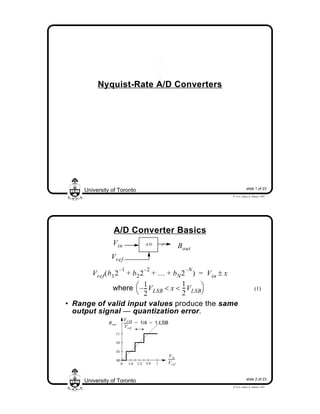
  • 1. University of Toronto slide 1 of 23 © D.A. Johns, K. Martin, 1997 Nyquist-Rate A/D Converters Vin A/D Vref Bout Vref b12–1 b22–2 … bN2–N ( + + + ) = Vin ± x -- – VLSB x 12 where 12    < < --VLSB Bout ---------- = 1/4 = 1 LSB 11 10 VLSB Vref University of Toronto slide 2 of 23 © D.A. Johns, K. Martin, 1997 A/D Converter Basics (1) • Range of valid input values produce the same output signal — quantization error. 01 00 0 1/4 1/2 Vin -------- Vref 3/4 1
  • 2. University of Toronto slide 3 of 23 © D.A. Johns, K. Martin, 1997 Analog to Digital Converters Low-to-Medium Speed, High Accuracy Medium Speed, Medium Accuracy High Speed, Low-to-Medium Accuracy Integrating Successive approximation Flash Oversampling (not Nyquist-rate) Algorithmic Two-step Interpolating Folding Pipelined Time-interleaved S2 V S1 – in Vref R1 C1 (Vin is held constant during conversion.) Control logic Counter b1 b2 b3 bN Comparator Clock fclk  S1  S2 1 Tclk = ----------- Vx Bout University of Toronto slide 4 of 23 © D.A. Johns, K. Martin, 1997 Integrating Converters • Low offset and gain errors for low-speed applications • Small amount of circuitry • Conversion speed is 2N+1 times 1/Tclk
  • 3. –Vin3 Phase (I) Phase (II) –Vin2 (Constant slope) University of Toronto slide 5 of 23 © D.A. Johns, K. Martin, 1997 Integrating Converters • Count at end of T2 is digital output • Does not depend on RC time-constant Time Vx T1 –Vin1 T2 (Three values for three inputs) H(f) –20 dB/decade slope 60 120 180 240 300 10 100 0 –10 –20 –30 (dB) Frequency (Hz) (Log scale) University of Toronto slide 6 of 23 © D.A. Johns, K. Martin, 1997 Integrating Converters • Notches the input frequencies which are multiples of 1/T1
  • 4. Successive-Approximation Converters Vin VD/A , = 0, i = 1 bi = 1 bi = 0 University of Toronto slide 7 of 23 © D.A. Johns, K. Martin, 1997 Sample Start Stop No Yes No Yes Signed input Vin VD/A > VD/A VD/A Vref 2→ + ⁄ i + 1 VD/A VD/A Vref 2→ – ( ⁄ i + 1) i → i + 1 i ≥ N •Makes use of binary search algorithm • /Requires N steps for N-bit converter • Successively “tunes” a signal until within 1 LSB of input •Medium speed •Moderate accuracy DAC Based Successive-Approximation S/H Successive-approximation register (SAR) and control logic b1 b2 bN D/A converter University of Toronto slide 8 of 23 © D.A. Johns, K. Martin, 1997 • Adjust until within 1 LSB of • Start with MSB and continue until LSB found • D/A mainly determines overall accuracy • Input S/H required Bout VD/A Vin Vref VD/A Vin
  • 5. SAR Vin Vref University of Toronto slide 9 of 23 © D.A. Johns, K. Martin, 1997 Charge Redistribution A/D 16C 8C 4C 2C C C 1. Sample mode 16C 8C 4C 2C C C 2. Hold mode 16C 8C 4C 2C C C 3. Bit cycling SAR SAR b1 b2 b3 b4 b5 s3 s1 s2 b1 b2 b3 b4 b5 s3 s1 s2 b1 b2 b3 b4 b5 s3 s1 s2 Vx ≅ 0 Vx = –Vin Vx – Vin Vref 2 = + ----------- Vin Vref Vin Vref University of Toronto slide 10 of 23 © D.A. Johns, K. Martin, 1997 Charge Redistribution A/D • Combines S/H, D/A converter, and difference circuit • Sample mode: Caps charged to Vin , compar reset. • Hold mode: Caps switched to gnd so Vx = –Vin • Bit cycling: Cap switched to Vref . If Vx < 0 cap left connected to Vref and bit=1. Otherwise, cap back to gnd and bit=0. Repeat N times • Cap bottom plates connected to Vref side to minimize parasitic capacitance at Vx . Parasitic cap does not cause conversion errors but it attenuates . Vx
  • 6. Algorithmic (or Cyclic) A/D Converter Start bi = 1 bi = 0 University of Toronto slide 11 of 23 © D.A. Johns, K. Martin, 1997 Sample V = Vin, i = 1 V > 0 V → 2(V – Vref /4) V → 2(V + Vref /4) i → i + 1 i > N Stop No Yes No Yes Signed input •Operates similar to successive-approx converter • Successive-approx halves ref voltage each cycle •Algorithmic doubles error each cycle (leaving ref voltage unchanged) Ratio-Independent Algorithmic Converter Out • Small amount of circuitry — reuse cyclically in time • Requires a high-precision multiply by 2 gain stage University of Toronto slide 12 of 23 © D.A. Johns, K. Martin, 1997 S/H X2 S/H Cmp Vref /4 –Vref /4 Vin Shift register Gain amp
  • 7. Ratio-Independent Algorithmic Converter Q1 Vout = 2 Verr • Does not rely on cap matching • Sample input twice using C1; hold first charge in C2 and re-combine with first charge on C1 University of Toronto slide 13 of 23 © D.A. Johns, K. Martin, 1997 Cmp Verr C1 Q1 C2 1. Sample remainder and cancel input-offset voltage. Cmp Verr C1 Q1 C2 2. Transfer charge Q1 from C1 to C2. Q1 Cmp Verr C1 Q2 C2 3. Sample input signal with C1 again Cmp Verr C1 Q1+Q2 C2 4. Combine Q1 and Q2 on C1, and connect C1 to output. after storing charge Q1 on C2. University of Toronto slide 14 of 23 © D.A. Johns, K. Martin, 1997 Flash (or Parallel) Converters Vref Vin (2N–1) to N encoder N digital outputs Over range Vr7 Vr6 Vr5 Vr4 Vr3 Vr2 Comparators R R R R R R R Vr1 R 2 ---- R ⁄ 2 •High-speed • Large size and power hungry • 2N comparators • Speed bottleneck usually large cap load at input • Thermometer code out of comps •Nands used for simpler decoding and/or bubble error correction •Use comp offset cancellation
  • 8. Issues in Designing Flash A/D Converters • Input Capacitive Loading— use interpolating arch. • Resistor-String Bowing — Due to Iin of bipolar comps — force center tap (or more) to be correct. • Signal and/or Clock Delay — Small arrival diff in clock or input cause errors. (250MHz 8-bit A/D needs 5ps matching for 1LSB) — route clock and Vin together with the delays matched [Gendai, 1991]. Match capacitive loads • Substrate and Power-Supply Noise — Vref = 2 V and 8-bit, 7.8 mV of noise causes 1 LSB error — shield clocks and use on-chip supply cap bypass • Flashback — Glitch at input due to going from track to latch mode — use preamps in comparators and match input impedances University of Toronto slide 15 of 23 © D.A. Johns, K. Martin, 1997 Flash Converters — Bubble Errors • Thermometer code should be 1111110000 • Bubble error (noise, metastability)— 1111110100 • Usually occurs near transition point but can cause gross errors depending on encoder University of Toronto slide 16 of 23 © D.A. Johns, K. Martin, 1997
  • 9. University of Toronto slide 17 of 23 © D.A. Johns, K. Martin, 1997 (2N–1) to N encoder N digital outputs Vin Vri … … … … … … … 4-bit A/D V1 Vin Vq 4-bit D/A 16 First 4 bits Vin Gain amp MSB 4-bit LSB A/D Lower 4 bits (b1, b2, b3, b4) (b5, b6, b7, b8) University of Toronto slide 18 of 23 © D.A. Johns, K. Martin, 1997 Two-Step A/D Converters • High-speed, medium accuracy (but 1 sample latency) • Less area and power than flash • Only 32 comparators in above 8-bit two-step • Gain amp likely sets speed limit • Without digital error correction, many blocks need at least 8-bit accuracy
  • 10. S/H1 Vin Vq MSB 4-bit A/D S/H2 4-bit D/A 8 S/H3 Error Digital delay D correction 8 bits 4 bits University of Toronto slide 19 of 23 © D.A. Johns, K. Martin, 1997 Digital Error Correction • Relaxes requirements on input A/D • Requires a 5-bit 2nd stage since Vq increased 5 bits Vin Gain amp (4-bit accurate) (8-bit accurate) (5-bit accurate) (5-bit accurate) (8-bit accurate) (8-bit accurate) V1 5-bit LSB A/D 0.75 V 0.5 V 0.25 V V4 V3 V2 V2b V2a R R R R R R R R R R R R R R 16 15 14 13 12 11 10 9 8 7 6 5 4 3 2 University of Toronto slide 20 of 23 © D.A. Johns, K. Martin, 1997 Interpolating A/D Converters Vref = 1 V Vin R R R R latch latch latch latch latch latch latch latch latch latch latch latch latch latch latch latch Digital logic b1 b2 b3 b4 (Overflow) Input amplifiers Latch comparators V1 R V2c R 1 •Use input amps to amplify input around reference voltages •Latch thresholds less critical •Less cap on input (faster than flash) •Match delays to latches •Often combined with folding architecture
  • 11. 5.0 V2 University of Toronto slide 21 of 23 © D.A. Johns, K. Martin, 1997 Interpolating Converters Vin 1.0 (Volts) (Volts) 0 0.25 0.5 0.75 0 V1 Latch threshold V2a V2b V2c QN DN QN-1 DN-2 Q1 QN-1 Q1 Q1 N – 1-bit shift register b1 b2 bN – 1 bN University of Toronto slide 22 of 23 © D.A. Johns, K. Martin, 1997 Pipelined A/D Converters D1 D1 D1 DN-2 1-bit DAPRX 1-bit DAPRX 1-bit DAPRX 1-bit DAPRX Vin Analog pipeline(DAPRX - digital approximator) S/H 2 Cmp –Vref/4 Vref/4 Vi–1 Vi bi
  • 12. Time-Interleaved A/D Converters [Black, 80] f1 S/H • Use parallel A/Ds and multiplex them • Tone occurs at fs/N for N converters if mismatched • Input S/H critical, others not — perhaps different tech for input S/H University of Toronto slide 23 of 23 © D.A. Johns, K. Martin, 1997 S/H S/H S/H S/H N-bit A/D N-bit A/D N-bit A/D N-bit A/D Dig. mux Digital output f2 f3 f4 f0 Vin