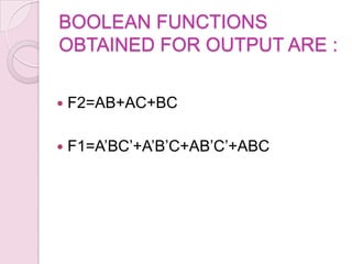
Downloaded 673 times


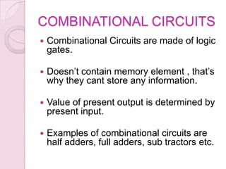
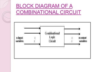
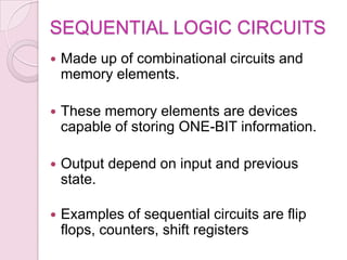
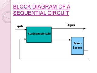
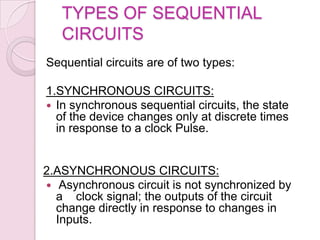
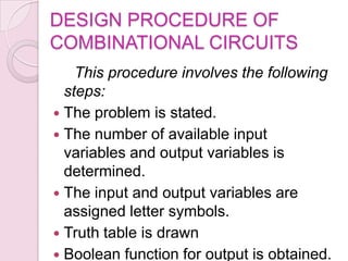
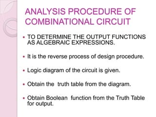
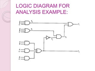
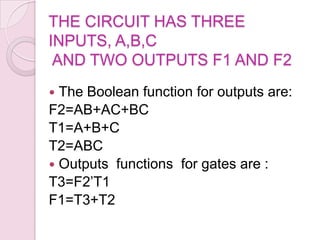
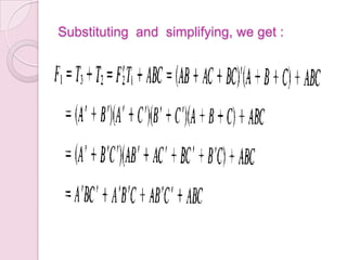
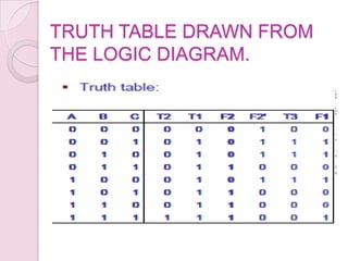


This document introduces digital logic circuits, including combinational and sequential circuits. It discusses that combinational circuits contain only logic gates and their output depends solely on present inputs. Sequential circuits contain both logic gates and memory elements, so their output depends on present inputs and previous states. The document outlines the design and analysis procedures for combinational circuits and provides examples of their block diagrams. It also describes synchronous and asynchronous sequential circuits.