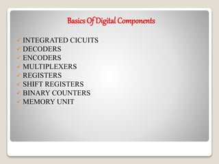
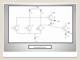
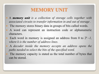
SlideShare a Scribd company logo
DIGITAL PRINCIPLES & COMPUTER
ORGANIZATION
DIGITAL COMPONENTS
Unit II
Submitted by
K.Lalithambiga.,Msc(cs),
Nadar Saraswathi College of Arts & Science,
Theni.
BasicsOf Digital Components
 INTEGRATED CICUITS
 DECODERS
 ENCODERS
 MULTIPLEXERS
 REGISTERS
 SHIFT REGISTERS
 BINARY COUNTERS
 MEMORY UNIT
INTEGRATED CICUITS (IC)
 An integrated circuit (IC) is a small silicon
semiconductor crystal, called a chip, containing the
electronic components for the digital gates.
 The various gates are interconnected inside the chip to
form the required circuit.
 The chip is mounted in a ceramic or plastic container,
and connections are welded by thin gold wires to external
pins to form the IC.
 The number of pins range from 14 to 100.
 Each IC has a numeric designation.
CATEGORIES
1. SSI(Small Scale Integration Device)
2. MSI(Medium Scale Integration Device)
3. LSI(Large Scale Integration Device)
4. VLSI(Very Large Scale Integration
Device)
5. ULSI(Ultra Large Scale Integration
Device)
SSI(Small Scale Integration Device)
 It contains several independent gates in a single package.
 The inputs and outputs of gates are connected directly to
the pins in the package.
 The number of gates is usually less than 10.
MSI(Medium Scale Integration Device)
 It contains 10 to 200 gates in a single package.
 They perform elementary digital functions such as
decoders, adders, registers.
LSI(Large Scale Integration Device)
 It contains gates between 200 to few thousand in a single
package.
 They include digital systems such as processors, memory
chips etc.
VLSI(Very Large Scale Integration Device)
 It contains thousands of gates within a single package
such as microcomputer chip.
ULSI(Ultra Large Scale Integration Device)
 It contains hundred of thousands of gates within a single
package such as microcomputer chip.
Digital Logic Family
 IC's are also classified by the specific circuit technology
to which they belong.
 The basic circuit in each technology
is NAND, NOR, NOT gates.
 The earliest logic family was Resistor-transistor
logic which used a resistor as input and a transistor as
switching device.
 Diode-transistor logic is a direct ancestor of the
Transistor-transistor logic, and used a diode for logic
functions while a transistor for amplifying functions.
TTL(Transistor Transistor Logic)
 It is the modified form of DTL(Diode Transistor Logic),
invented in 1961 by James L Buie.
 The diodes were replaced by transistor to improve the
circuit operation. It is called transistor-transistor logic
because transistor performs both the logic function and
the amplifying function.
Advantages:
 TTL circuits are fast.
 Low propagation delay.
 Power dissipation does not depend upon the frequency.
Two is inputs TTL NAND gate with one output
ECL(Emitter Coupled Logic)
 It provides highest speed digital circuits.
 It is used in systems such as supercomputers and signal
processors where high speed is required.
 ECL uses overdriven BJT(Bipolar junction Transistors)
in its circuit.
Advantages:
 ECL is the fastest logic family.
 Propagation delay is very less.
 Noise margin is low.
two input ECL gate
MOS(Metal Oxide Semiconductor)
PMOS NMOS
•MOS depends upon the flow of one type of
carriers (electrons or holes). It is basically of two
types:
A p-channel MOS is
called PMOS.
Transistors operate by
creating an inversion
layer in an n-type
transistor body.
A n-channel MOS is
called NMOS.
Transistors functions
by creating an n-
channel(inversion layer)
in a p-type transistor
body.
 FET(Field Effect Transistor) have 4 terminals:
Gate, Drain, Source and Substrate.
 They have four modes of operation:
 cut-off (or sub threshold),
 triode,
saturation (sometimes called active) and
velocity saturation.
CMOS(Complimentary MOS)
 CMOS used to construct Integrated Circuits.
 It uses both P and N channel MOS.
 It is also known as COS-MOS(Complementary-
symmetry metal oxide semiconductor)
 It uses complementary and symmetrical pairs of p-
type and n-type MOS for logic functions.
 It is used in systems which require low power
consumption.
Advantages:
 Noise margin is high.
 Power dissipation is low.
 Waste heat production is very less
as compared to other logic families.
 CMOS allows high density Integra
-tion of logic functions on a chip.
two input ECL gate
DECODERS
 A decoder is a combinational circuit that converts binary
information from n coded inputs to maximum 2n outputs.
 Commercial decoders include one or more enable (E)
inputs to control the operation of circuit.
 The decoder is enabled when E is equal to 1 and
disabled when E is equal to 0.
 Used in code converters.
 Used to Boolean functions.
ENCODERS
 An encoder is a digital circuit that performs the inverse
operation of a decoder.
 An encoder has 2n input lines and n output lines.
 It converts octal input to binary digits.
Types:
 Priority encoders.
 Decimal to BCD encoder.
 Octal to binary encoder.
 Hexadecimal to binary encoder.
MULTIPLEXERS
 A multiplexer is a combinational circuit that receives
binary information from one of the 2n input lines and
directs it to a single output line.
Advantages:
 It reduces number of wires.
 Circuit is less complex.
 Less costly.
 It is used to implement many circuits.
REGISTERS
 A register is a group of flip-flops with each flip-flop
capable of storing one bit of information.
 The register is mainly used for storing and shifting binary
data entered into it from an external sources.
 The register is a type of sequential circuit and an
important building block used in digital system like
multipliers, dividers, memories, microprocessors, etc.,
4-bit register
SHIFT REGISTERS
 A shift register is capable of shifting its binary information
either to the right or left is called shift register.
 The shift register permits the stored data to move from a
particular location to another location within the register.
 There is two method shifting the data
 Serial shifting .
 Parallel shifting.
 The serial shifting method shifts one bit at a time for each
clock pulse in a serial fashion, beginning with either MSB or
LSB.
 The parallel shifting operation all the data (I/O)get shifted
simultaneously during a single clock pulse.
Serial Input Serial Output(siso)
 Let all the flip-flop be initially in the reset condition i.e. Q3 = Q2 =
Q1 = Q0 = 0.
 If an entry of a four bit binary number 1 1 1 1 is made into the
register, this number should be applied to Din bit with the LSB bit
applied first. The D input of FF-3 i.e. D3 is connected to serial data
input Din.
 Output of FF-3 i.e. Q3 is connected to the input of the next flip-flop
i.e. D2 and so on.
Serial Input Parallel Output(sipo)
 The data is entered serially and taken out in parallel fashion.
 Data is loaded bit by bit. The outputs are disabled as long as the
data is loading.
 As soon as the data loading gets completed, all the flip-flops
contain their required data.
 The outputs are enabled so that all the loaded data is made
available over all the output lines at the same time.
 4 clock cycles are required to load a four bit word.
 Hence the speed of operation of SIPO mode is same as that of
SISO mode.
Parallel Input Serial Output (PISO)
 Data bits are entered in parallel fashion.
 The circuit shown below is a four bit parallel input serial output
register.
 Output of previous Flip Flop is connected to the input of the next one
via a combinational circuit.
 The binary input word B0, B1, B2, B3 is applied though the same
combinational circuit.
 There are two modes in which this circuit can work namely - shift
mode or load mode.
Parallel Input Parallel Output (PIPO)
 In this mode, the 4 bit binary input B0, B1, B2, B3 is applied to
the data inputs D0, D1, D2, D3 respectively of the four flip-flops.
 As soon as a negative clock edge is applied, the input binary bits
will be loaded into the flip-flops simultaneously.
 The loaded bits will appear simultaneously to the output side.
Only clock pulse is essential to load all the bits.
counters
 Binary counter- A counter that follows the binary number
sequence is called a binary counter.
Counters are available in two categories
 Ripple Counters-A register that goes through a prescribed
sequence of states upon the application of input pulse is called a
counter.
 Synchronous counters- In this clock pulses are applied to the
inputs of all flip-flops.
 A common clock triggers all flip-flops simultaneously rather than
one at a time in succession as in a ripple counter.
 BCD Ripple Counter-A decimal counter follows a sequence of
ten states and returns to 0 after the count of 9.
 Up-Down Binary Counter-The two operations can be combined
in one circuit to form a counter capable of counting up or down.
 It has an up control input and down control input.
 Binary Counter with Parallel Load-A counter with parallel load
can be used to generate any desire count sequence.
 Is used to generate the BCD count. up control input and down
control input.
 Ring Counter- A ring counter is a circular shift register with only
one flip-flop being set at any particular time, all others are
cleared.
 The single bit is shifted from one flip-flop to the next to produce
the sequence
 Johnson Counter-Generate the timing signals with a combination
of a shift register and a decoder, which is called a Johnson
counter.
 The number of states can be double if the shift register is connect
as a switch-tail ring counter of timing signals.
 HDL for Registers and Counters-Registers and counters can be
describe in HDL at either the behavioral or the structural level.
MEMORY UNIT
 A memory unit is a collection of storage cells together with
associated circuits to transfer information in and out of storage .
 The memory stores binary data in groups of bits called words.
 A word can represent an instruction code or alphanumeric
characters.
 Each word in memory is assigned an address from 0 to 2k –1,
where k is the number of address lines.
 A decoder inside the memory accepts an address opens the
paths needed to select the bits of the specified word.
 The memory capacity is stated as the total number of bytes that
can be stored.
 In random-access memory (RAM) the memory cells can
be accessed for information from any desired random
location.
 The process of locating a word in memory is the same and
requires an equal amount of time no matter where the cells
are located physically in memory.
 Communication between memory and its environment is
achieved via data input and output lines, address selections
lines, and control lines.
 The n data input lines provide the information to be
stored in memory.
 The n data output lines supply the information
coming out of memory.
 The k address lines provide a binary number of k
bits that specify a specific word or location .
 The two control lines specify the direction of
transfer – either read or write.
Block diagram of random access memory(RAM)
Steps to write to memory:
Apply the binary
address of the desired
word into the address
lines.
Apply the data bits that
are to be stored in
memory on the data
lines.
Activate the write input.
Steps to read from memory:
Apply the binary address of
the desired word into the
address lines.
 Activate the read input
A read-only memory (ROM)
is a memory unit that
performs the read operation
only – there is no write
capability .
The binary information
stored in a ROM is permanent
during the hardware
production.
 RAM is a general-purpose device whose contents can be
altered.
 The information in ROM forms the required
interconnection pattern.
 ROMs come with special internal electronic fuses that
can be programmed for a specific configuration.
 An m x n ROM is an array of binary cells organized into
m words of n bits each.
 A ROM has k address lines to select one of m words
in memory and n output lines, one for each bit of the
word.
 May have one or more enable inputs for expansion.
 The outputs are a function of only the present input
(the address), so it is a combinational circuit
constructed of decoders and OR gates.
Block diagram of read only memory (ROM)
 When used as a memory unit, it stores fixed programs
that are not to be altered and for tables of constants that
will not change .
 When used in the design of control units for digital
computers, it stores coded information that represents the
sequence of internal control variables to enable the
various operations .
 A control unit that utilizes a ROM is called a micro
programmed control unit .
The required paths may be programmed in three different
ways :
 Mask programming is done by the semiconductor
company based upon a truth table provided by the
manufacturer.
 Programmable read-only memory (PROM) is more
economical. PROM units contain all fuses intact and are
blown by users.
 Erasable PROM (EPROM) can be altered using a
special ultraviolet light .
 Electrical erasable PROM (EEPROM) can be erased
with electrical signals .
Digital Components

More Related Content

What's hot

Assembly Language and microprocessor
Assembly Language and microprocessorAssembly Language and microprocessor
Assembly Language and microprocessor
Khaled Sany
 
8086 micro processor
8086 micro processor8086 micro processor
8086 micro processor
Poojith Chowdhary
 
Sequential circuits in Digital Electronics
Sequential circuits in Digital ElectronicsSequential circuits in Digital Electronics
Sequential circuits in Digital Electronics
Vinoth Loganathan
 
8257 DMA Controller
8257 DMA Controller8257 DMA Controller
8257 DMA Controller
ShivamSood22
 
8086 pin diagram description
8086 pin diagram description8086 pin diagram description
8086 pin diagram description
Akhil Singal
 
Register in Digital Logic
Register in Digital LogicRegister in Digital Logic
Register in Digital Logic
ISMT College
 
8051 timer counter
8051 timer counter8051 timer counter
8051 timer counter
vishalgohel12195
 
4 bit Binary counter
4 bit Binary counter4 bit Binary counter
4 bit Binary counter
Jainee Solanki
 
8086 microprocessor-architecture
8086 microprocessor-architecture8086 microprocessor-architecture
8086 microprocessor-architecture
prasadpawaskar
 
Flipflop
FlipflopFlipflop
Flipflop
sohamdodia27
 
Register transfer language & its micro operations
Register transfer language & its micro operationsRegister transfer language & its micro operations
Register transfer language & its micro operations
Lakshya Sharma
 
Flip-Flop || Digital Electronics
Flip-Flop || Digital ElectronicsFlip-Flop || Digital Electronics
Flip-Flop || Digital Electronics
Md Sadequl Islam
 
8051 MICROCONTROLLER
8051 MICROCONTROLLER 8051 MICROCONTROLLER
8051 MICROCONTROLLER
THANDAIAH PRABU
 
3.programmable interrupt controller 8259
3.programmable interrupt controller 82593.programmable interrupt controller 8259
3.programmable interrupt controller 8259
MdFazleRabbi18
 
Timing diagram 8085 microprocessor
Timing diagram 8085 microprocessorTiming diagram 8085 microprocessor
Timing diagram 8085 microprocessor
Velalar College of Engineering and Technology
 
Memory & I/O interfacing
Memory & I/O  interfacingMemory & I/O  interfacing
Memory & I/O interfacing
deval patel
 
Interrupts of 8086
Interrupts of 8086Interrupts of 8086
Interrupts of 8086
Albin Panakkal
 
Latches and flip flop
Latches and flip flopLatches and flip flop
Latches and flip flop
Shuaib Hotak
 
bus and memory tranfer (computer organaization)
bus and memory tranfer (computer organaization)bus and memory tranfer (computer organaization)
bus and memory tranfer (computer organaization)
Siddhi Viradiya
 
Architecture of 8086 Microprocessor
Architecture of 8086 Microprocessor  Architecture of 8086 Microprocessor
Architecture of 8086 Microprocessor Mustapha Fatty
 

What's hot (20)

Assembly Language and microprocessor
Assembly Language and microprocessorAssembly Language and microprocessor
Assembly Language and microprocessor
 
8086 micro processor
8086 micro processor8086 micro processor
8086 micro processor
 
Sequential circuits in Digital Electronics
Sequential circuits in Digital ElectronicsSequential circuits in Digital Electronics
Sequential circuits in Digital Electronics
 
8257 DMA Controller
8257 DMA Controller8257 DMA Controller
8257 DMA Controller
 
8086 pin diagram description
8086 pin diagram description8086 pin diagram description
8086 pin diagram description
 
Register in Digital Logic
Register in Digital LogicRegister in Digital Logic
Register in Digital Logic
 
8051 timer counter
8051 timer counter8051 timer counter
8051 timer counter
 
4 bit Binary counter
4 bit Binary counter4 bit Binary counter
4 bit Binary counter
 
8086 microprocessor-architecture
8086 microprocessor-architecture8086 microprocessor-architecture
8086 microprocessor-architecture
 
Flipflop
FlipflopFlipflop
Flipflop
 
Register transfer language & its micro operations
Register transfer language & its micro operationsRegister transfer language & its micro operations
Register transfer language & its micro operations
 
Flip-Flop || Digital Electronics
Flip-Flop || Digital ElectronicsFlip-Flop || Digital Electronics
Flip-Flop || Digital Electronics
 
8051 MICROCONTROLLER
8051 MICROCONTROLLER 8051 MICROCONTROLLER
8051 MICROCONTROLLER
 
3.programmable interrupt controller 8259
3.programmable interrupt controller 82593.programmable interrupt controller 8259
3.programmable interrupt controller 8259
 
Timing diagram 8085 microprocessor
Timing diagram 8085 microprocessorTiming diagram 8085 microprocessor
Timing diagram 8085 microprocessor
 
Memory & I/O interfacing
Memory & I/O  interfacingMemory & I/O  interfacing
Memory & I/O interfacing
 
Interrupts of 8086
Interrupts of 8086Interrupts of 8086
Interrupts of 8086
 
Latches and flip flop
Latches and flip flopLatches and flip flop
Latches and flip flop
 
bus and memory tranfer (computer organaization)
bus and memory tranfer (computer organaization)bus and memory tranfer (computer organaization)
bus and memory tranfer (computer organaization)
 
Architecture of 8086 Microprocessor
Architecture of 8086 Microprocessor  Architecture of 8086 Microprocessor
Architecture of 8086 Microprocessor
 

Similar to Digital Components

Computer System and Architecture
Computer System and ArchitectureComputer System and Architecture
Computer System and Architecture
sarfraz1411
 
Cs302 shortnoteslectures1to45
Cs302 shortnoteslectures1to45Cs302 shortnoteslectures1to45
Cs302 shortnoteslectures1to45
javediqbalmirza
 
Combinational circuits
Combinational circuitsCombinational circuits
Combinational circuits
Nabarun Chakraborty
 
Interfacing of data converters & io devices
Interfacing of data converters & io devicesInterfacing of data converters & io devices
Interfacing of data converters & io devices
Dr.YNM
 
ATT SMK.pptx
ATT SMK.pptxATT SMK.pptx
ATT SMK.pptx
MadhavKarve
 
Design of Counter Using SRAM
Design of Counter Using SRAMDesign of Counter Using SRAM
Design of Counter Using SRAM
IOSRJECE
 
STLD-Combinational logic design
STLD-Combinational  logic design STLD-Combinational  logic design
STLD-Combinational logic design
Abhinay Potlabathini
 
digital elctronics
digital elctronicsdigital elctronics
digital elctronics
Asif Iqbal
 
Research Inventy : International Journal of Engineering and Science is publis...
Research Inventy : International Journal of Engineering and Science is publis...Research Inventy : International Journal of Engineering and Science is publis...
Research Inventy : International Journal of Engineering and Science is publis...researchinventy
 
Research Inventy: International Journal of Engineering and Science
Research Inventy: International Journal of Engineering and ScienceResearch Inventy: International Journal of Engineering and Science
Research Inventy: International Journal of Engineering and Scienceresearchinventy
 
Chapter 1.pptx
Chapter 1.pptxChapter 1.pptx
Chapter 1.pptx
abdirahman gure
 
Training Report on embedded Systems and Robotics
Training Report on embedded  Systems and RoboticsTraining Report on embedded  Systems and Robotics
Training Report on embedded Systems and Robotics
NIT Raipur
 
ALU project(segma team)
ALU project(segma team)ALU project(segma team)
ALU project(segma team)
Mohamed Seif
 
Module 4 registers and counters
Module 4 registers and counters Module 4 registers and counters
Module 4 registers and counters
Deepak John
 
Registers and counters
Registers and counters Registers and counters
Registers and counters Deepak John
 
FYBSC IT Digital Electronics Unit V Chapter II Shift Register
FYBSC IT Digital Electronics Unit V Chapter II Shift RegisterFYBSC IT Digital Electronics Unit V Chapter II Shift Register
FYBSC IT Digital Electronics Unit V Chapter II Shift Register
Arti Parab Academics
 
FYBSC IT Digital Electronics Unit V Chapter I Counters
FYBSC IT Digital Electronics Unit V Chapter I CountersFYBSC IT Digital Electronics Unit V Chapter I Counters
FYBSC IT Digital Electronics Unit V Chapter I Counters
Arti Parab Academics
 
Registers and counters
Registers and countersRegisters and counters
Registers and counters
Heman Pathak
 
Digital logic-formula-notes-final-1
Digital logic-formula-notes-final-1Digital logic-formula-notes-final-1
Digital logic-formula-notes-final-1
Kshitij Singh
 

Similar to Digital Components (20)

Computer System and Architecture
Computer System and ArchitectureComputer System and Architecture
Computer System and Architecture
 
Cs302 shortnoteslectures1to45
Cs302 shortnoteslectures1to45Cs302 shortnoteslectures1to45
Cs302 shortnoteslectures1to45
 
Combinational circuits
Combinational circuitsCombinational circuits
Combinational circuits
 
Interfacing of data converters & io devices
Interfacing of data converters & io devicesInterfacing of data converters & io devices
Interfacing of data converters & io devices
 
ATT SMK.pptx
ATT SMK.pptxATT SMK.pptx
ATT SMK.pptx
 
Design of Counter Using SRAM
Design of Counter Using SRAMDesign of Counter Using SRAM
Design of Counter Using SRAM
 
STLD-Combinational logic design
STLD-Combinational  logic design STLD-Combinational  logic design
STLD-Combinational logic design
 
digital elctronics
digital elctronicsdigital elctronics
digital elctronics
 
Research Inventy : International Journal of Engineering and Science is publis...
Research Inventy : International Journal of Engineering and Science is publis...Research Inventy : International Journal of Engineering and Science is publis...
Research Inventy : International Journal of Engineering and Science is publis...
 
Research Inventy: International Journal of Engineering and Science
Research Inventy: International Journal of Engineering and ScienceResearch Inventy: International Journal of Engineering and Science
Research Inventy: International Journal of Engineering and Science
 
Chapter 1.pptx
Chapter 1.pptxChapter 1.pptx
Chapter 1.pptx
 
Training Report on embedded Systems and Robotics
Training Report on embedded  Systems and RoboticsTraining Report on embedded  Systems and Robotics
Training Report on embedded Systems and Robotics
 
ALU project(segma team)
ALU project(segma team)ALU project(segma team)
ALU project(segma team)
 
Module 4 registers and counters
Module 4 registers and counters Module 4 registers and counters
Module 4 registers and counters
 
Registers and counters
Registers and counters Registers and counters
Registers and counters
 
FYBSC IT Digital Electronics Unit V Chapter II Shift Register
FYBSC IT Digital Electronics Unit V Chapter II Shift RegisterFYBSC IT Digital Electronics Unit V Chapter II Shift Register
FYBSC IT Digital Electronics Unit V Chapter II Shift Register
 
FYBSC IT Digital Electronics Unit V Chapter I Counters
FYBSC IT Digital Electronics Unit V Chapter I CountersFYBSC IT Digital Electronics Unit V Chapter I Counters
FYBSC IT Digital Electronics Unit V Chapter I Counters
 
Registers and counters
Registers and countersRegisters and counters
Registers and counters
 
Digital logic-formula-notes-final-1
Digital logic-formula-notes-final-1Digital logic-formula-notes-final-1
Digital logic-formula-notes-final-1
 
Dns module3 p3
Dns module3 p3Dns module3 p3
Dns module3 p3
 

More from lalithambiga kamaraj

Firewall in Network Security
Firewall in Network SecurityFirewall in Network Security
Firewall in Network Security
lalithambiga kamaraj
 
Data Compression in Multimedia
Data Compression in MultimediaData Compression in Multimedia
Data Compression in Multimedia
lalithambiga kamaraj
 
Data CompressionMultimedia
Data CompressionMultimediaData CompressionMultimedia
Data CompressionMultimedia
lalithambiga kamaraj
 
Digital Audio in Multimedia
Digital Audio in MultimediaDigital Audio in Multimedia
Digital Audio in Multimedia
lalithambiga kamaraj
 
Network Security: Physical security
Network Security: Physical security Network Security: Physical security
Network Security: Physical security
lalithambiga kamaraj
 
Graphs in Data Structure
Graphs in Data StructureGraphs in Data Structure
Graphs in Data Structure
lalithambiga kamaraj
 
Package in Java
Package in JavaPackage in Java
Package in Java
lalithambiga kamaraj
 
Exception Handling in Java
Exception Handling in JavaException Handling in Java
Exception Handling in Java
lalithambiga kamaraj
 
Data structure
Data structureData structure
Data structure
lalithambiga kamaraj
 
Digital Image Processing
Digital Image ProcessingDigital Image Processing
Digital Image Processing
lalithambiga kamaraj
 
Digital Image Processing
Digital Image ProcessingDigital Image Processing
Digital Image Processing
lalithambiga kamaraj
 
Estimating Software Maintenance Costs
Estimating Software Maintenance CostsEstimating Software Maintenance Costs
Estimating Software Maintenance Costs
lalithambiga kamaraj
 
Datamining
DataminingDatamining
Deadlocks in operating system
Deadlocks in operating systemDeadlocks in operating system
Deadlocks in operating system
lalithambiga kamaraj
 
Io management disk scheduling algorithm
Io management disk scheduling algorithmIo management disk scheduling algorithm
Io management disk scheduling algorithm
lalithambiga kamaraj
 
Recovery system
Recovery systemRecovery system
Recovery system
lalithambiga kamaraj
 
File management
File managementFile management
File management
lalithambiga kamaraj
 
Preprocessor
PreprocessorPreprocessor
Preprocessor
lalithambiga kamaraj
 
Inheritance
InheritanceInheritance
Managing console of I/o operations & working with files
Managing console of I/o operations & working with filesManaging console of I/o operations & working with files
Managing console of I/o operations & working with files
lalithambiga kamaraj
 

More from lalithambiga kamaraj (20)

Firewall in Network Security
Firewall in Network SecurityFirewall in Network Security
Firewall in Network Security
 
Data Compression in Multimedia
Data Compression in MultimediaData Compression in Multimedia
Data Compression in Multimedia
 
Data CompressionMultimedia
Data CompressionMultimediaData CompressionMultimedia
Data CompressionMultimedia
 
Digital Audio in Multimedia
Digital Audio in MultimediaDigital Audio in Multimedia
Digital Audio in Multimedia
 
Network Security: Physical security
Network Security: Physical security Network Security: Physical security
Network Security: Physical security
 
Graphs in Data Structure
Graphs in Data StructureGraphs in Data Structure
Graphs in Data Structure
 
Package in Java
Package in JavaPackage in Java
Package in Java
 
Exception Handling in Java
Exception Handling in JavaException Handling in Java
Exception Handling in Java
 
Data structure
Data structureData structure
Data structure
 
Digital Image Processing
Digital Image ProcessingDigital Image Processing
Digital Image Processing
 
Digital Image Processing
Digital Image ProcessingDigital Image Processing
Digital Image Processing
 
Estimating Software Maintenance Costs
Estimating Software Maintenance CostsEstimating Software Maintenance Costs
Estimating Software Maintenance Costs
 
Datamining
DataminingDatamining
Datamining
 
Deadlocks in operating system
Deadlocks in operating systemDeadlocks in operating system
Deadlocks in operating system
 
Io management disk scheduling algorithm
Io management disk scheduling algorithmIo management disk scheduling algorithm
Io management disk scheduling algorithm
 
Recovery system
Recovery systemRecovery system
Recovery system
 
File management
File managementFile management
File management
 
Preprocessor
PreprocessorPreprocessor
Preprocessor
 
Inheritance
InheritanceInheritance
Inheritance
 
Managing console of I/o operations & working with files
Managing console of I/o operations & working with filesManaging console of I/o operations & working with files
Managing console of I/o operations & working with files
 

Recently uploaded

Thesis Statement for students diagnonsed withADHD.ppt
Thesis Statement for students diagnonsed withADHD.pptThesis Statement for students diagnonsed withADHD.ppt
Thesis Statement for students diagnonsed withADHD.ppt
EverAndrsGuerraGuerr
 
Home assignment II on Spectroscopy 2024 Answers.pdf
Home assignment II on Spectroscopy 2024 Answers.pdfHome assignment II on Spectroscopy 2024 Answers.pdf
Home assignment II on Spectroscopy 2024 Answers.pdf
Tamralipta Mahavidyalaya
 
The approach at University of Liverpool.pptx
The approach at University of Liverpool.pptxThe approach at University of Liverpool.pptx
The approach at University of Liverpool.pptx
Jisc
 
Chapter 3 - Islamic Banking Products and Services.pptx
Chapter 3 - Islamic Banking Products and Services.pptxChapter 3 - Islamic Banking Products and Services.pptx
Chapter 3 - Islamic Banking Products and Services.pptx
Mohd Adib Abd Muin, Senior Lecturer at Universiti Utara Malaysia
 
Mule 4.6 & Java 17 Upgrade | MuleSoft Mysore Meetup #46
Mule 4.6 & Java 17 Upgrade | MuleSoft Mysore Meetup #46Mule 4.6 & Java 17 Upgrade | MuleSoft Mysore Meetup #46
Mule 4.6 & Java 17 Upgrade | MuleSoft Mysore Meetup #46
MysoreMuleSoftMeetup
 
Overview on Edible Vaccine: Pros & Cons with Mechanism
Overview on Edible Vaccine: Pros & Cons with MechanismOverview on Edible Vaccine: Pros & Cons with Mechanism
Overview on Edible Vaccine: Pros & Cons with Mechanism
DeeptiGupta154
 
CLASS 11 CBSE B.St Project AIDS TO TRADE - INSURANCE
CLASS 11 CBSE B.St Project AIDS TO TRADE - INSURANCECLASS 11 CBSE B.St Project AIDS TO TRADE - INSURANCE
CLASS 11 CBSE B.St Project AIDS TO TRADE - INSURANCE
BhavyaRajput3
 
Language Across the Curriculm LAC B.Ed.
Language Across the  Curriculm LAC B.Ed.Language Across the  Curriculm LAC B.Ed.
Language Across the Curriculm LAC B.Ed.
Atul Kumar Singh
 
The French Revolution Class 9 Study Material pdf free download
The French Revolution Class 9 Study Material pdf free downloadThe French Revolution Class 9 Study Material pdf free download
The French Revolution Class 9 Study Material pdf free download
Vivekanand Anglo Vedic Academy
 
Honest Reviews of Tim Han LMA Course Program.pptx
Honest Reviews of Tim Han LMA Course Program.pptxHonest Reviews of Tim Han LMA Course Program.pptx
Honest Reviews of Tim Han LMA Course Program.pptx
timhan337
 
Biological Screening of Herbal Drugs in detailed.
Biological Screening of Herbal Drugs in detailed.Biological Screening of Herbal Drugs in detailed.
Biological Screening of Herbal Drugs in detailed.
Ashokrao Mane college of Pharmacy Peth-Vadgaon
 
June 3, 2024 Anti-Semitism Letter Sent to MIT President Kornbluth and MIT Cor...
June 3, 2024 Anti-Semitism Letter Sent to MIT President Kornbluth and MIT Cor...June 3, 2024 Anti-Semitism Letter Sent to MIT President Kornbluth and MIT Cor...
June 3, 2024 Anti-Semitism Letter Sent to MIT President Kornbluth and MIT Cor...
Levi Shapiro
 
Lapbook sobre os Regimes Totalitários.pdf
Lapbook sobre os Regimes Totalitários.pdfLapbook sobre os Regimes Totalitários.pdf
Lapbook sobre os Regimes Totalitários.pdf
Jean Carlos Nunes Paixão
 
Sha'Carri Richardson Presentation 202345
Sha'Carri Richardson Presentation 202345Sha'Carri Richardson Presentation 202345
Sha'Carri Richardson Presentation 202345
beazzy04
 
1.4 modern child centered education - mahatma gandhi-2.pptx
1.4 modern child centered education - mahatma gandhi-2.pptx1.4 modern child centered education - mahatma gandhi-2.pptx
1.4 modern child centered education - mahatma gandhi-2.pptx
JosvitaDsouza2
 
TESDA TM1 REVIEWER FOR NATIONAL ASSESSMENT WRITTEN AND ORAL QUESTIONS WITH A...
TESDA TM1 REVIEWER  FOR NATIONAL ASSESSMENT WRITTEN AND ORAL QUESTIONS WITH A...TESDA TM1 REVIEWER  FOR NATIONAL ASSESSMENT WRITTEN AND ORAL QUESTIONS WITH A...
TESDA TM1 REVIEWER FOR NATIONAL ASSESSMENT WRITTEN AND ORAL QUESTIONS WITH A...
EugeneSaldivar
 
The Accursed House by Émile Gaboriau.pptx
The Accursed House by Émile Gaboriau.pptxThe Accursed House by Émile Gaboriau.pptx
The Accursed House by Émile Gaboriau.pptx
DhatriParmar
 
How libraries can support authors with open access requirements for UKRI fund...
How libraries can support authors with open access requirements for UKRI fund...How libraries can support authors with open access requirements for UKRI fund...
How libraries can support authors with open access requirements for UKRI fund...
Jisc
 
How to Make a Field invisible in Odoo 17
How to Make a Field invisible in Odoo 17How to Make a Field invisible in Odoo 17
How to Make a Field invisible in Odoo 17
Celine George
 
2024.06.01 Introducing a competency framework for languag learning materials ...
2024.06.01 Introducing a competency framework for languag learning materials ...2024.06.01 Introducing a competency framework for languag learning materials ...
2024.06.01 Introducing a competency framework for languag learning materials ...
Sandy Millin
 

Recently uploaded (20)

Thesis Statement for students diagnonsed withADHD.ppt
Thesis Statement for students diagnonsed withADHD.pptThesis Statement for students diagnonsed withADHD.ppt
Thesis Statement for students diagnonsed withADHD.ppt
 
Home assignment II on Spectroscopy 2024 Answers.pdf
Home assignment II on Spectroscopy 2024 Answers.pdfHome assignment II on Spectroscopy 2024 Answers.pdf
Home assignment II on Spectroscopy 2024 Answers.pdf
 
The approach at University of Liverpool.pptx
The approach at University of Liverpool.pptxThe approach at University of Liverpool.pptx
The approach at University of Liverpool.pptx
 
Chapter 3 - Islamic Banking Products and Services.pptx
Chapter 3 - Islamic Banking Products and Services.pptxChapter 3 - Islamic Banking Products and Services.pptx
Chapter 3 - Islamic Banking Products and Services.pptx
 
Mule 4.6 & Java 17 Upgrade | MuleSoft Mysore Meetup #46
Mule 4.6 & Java 17 Upgrade | MuleSoft Mysore Meetup #46Mule 4.6 & Java 17 Upgrade | MuleSoft Mysore Meetup #46
Mule 4.6 & Java 17 Upgrade | MuleSoft Mysore Meetup #46
 
Overview on Edible Vaccine: Pros & Cons with Mechanism
Overview on Edible Vaccine: Pros & Cons with MechanismOverview on Edible Vaccine: Pros & Cons with Mechanism
Overview on Edible Vaccine: Pros & Cons with Mechanism
 
CLASS 11 CBSE B.St Project AIDS TO TRADE - INSURANCE
CLASS 11 CBSE B.St Project AIDS TO TRADE - INSURANCECLASS 11 CBSE B.St Project AIDS TO TRADE - INSURANCE
CLASS 11 CBSE B.St Project AIDS TO TRADE - INSURANCE
 
Language Across the Curriculm LAC B.Ed.
Language Across the  Curriculm LAC B.Ed.Language Across the  Curriculm LAC B.Ed.
Language Across the Curriculm LAC B.Ed.
 
The French Revolution Class 9 Study Material pdf free download
The French Revolution Class 9 Study Material pdf free downloadThe French Revolution Class 9 Study Material pdf free download
The French Revolution Class 9 Study Material pdf free download
 
Honest Reviews of Tim Han LMA Course Program.pptx
Honest Reviews of Tim Han LMA Course Program.pptxHonest Reviews of Tim Han LMA Course Program.pptx
Honest Reviews of Tim Han LMA Course Program.pptx
 
Biological Screening of Herbal Drugs in detailed.
Biological Screening of Herbal Drugs in detailed.Biological Screening of Herbal Drugs in detailed.
Biological Screening of Herbal Drugs in detailed.
 
June 3, 2024 Anti-Semitism Letter Sent to MIT President Kornbluth and MIT Cor...
June 3, 2024 Anti-Semitism Letter Sent to MIT President Kornbluth and MIT Cor...June 3, 2024 Anti-Semitism Letter Sent to MIT President Kornbluth and MIT Cor...
June 3, 2024 Anti-Semitism Letter Sent to MIT President Kornbluth and MIT Cor...
 
Lapbook sobre os Regimes Totalitários.pdf
Lapbook sobre os Regimes Totalitários.pdfLapbook sobre os Regimes Totalitários.pdf
Lapbook sobre os Regimes Totalitários.pdf
 
Sha'Carri Richardson Presentation 202345
Sha'Carri Richardson Presentation 202345Sha'Carri Richardson Presentation 202345
Sha'Carri Richardson Presentation 202345
 
1.4 modern child centered education - mahatma gandhi-2.pptx
1.4 modern child centered education - mahatma gandhi-2.pptx1.4 modern child centered education - mahatma gandhi-2.pptx
1.4 modern child centered education - mahatma gandhi-2.pptx
 
TESDA TM1 REVIEWER FOR NATIONAL ASSESSMENT WRITTEN AND ORAL QUESTIONS WITH A...
TESDA TM1 REVIEWER  FOR NATIONAL ASSESSMENT WRITTEN AND ORAL QUESTIONS WITH A...TESDA TM1 REVIEWER  FOR NATIONAL ASSESSMENT WRITTEN AND ORAL QUESTIONS WITH A...
TESDA TM1 REVIEWER FOR NATIONAL ASSESSMENT WRITTEN AND ORAL QUESTIONS WITH A...
 
The Accursed House by Émile Gaboriau.pptx
The Accursed House by Émile Gaboriau.pptxThe Accursed House by Émile Gaboriau.pptx
The Accursed House by Émile Gaboriau.pptx
 
How libraries can support authors with open access requirements for UKRI fund...
How libraries can support authors with open access requirements for UKRI fund...How libraries can support authors with open access requirements for UKRI fund...
How libraries can support authors with open access requirements for UKRI fund...
 
How to Make a Field invisible in Odoo 17
How to Make a Field invisible in Odoo 17How to Make a Field invisible in Odoo 17
How to Make a Field invisible in Odoo 17
 
2024.06.01 Introducing a competency framework for languag learning materials ...
2024.06.01 Introducing a competency framework for languag learning materials ...2024.06.01 Introducing a competency framework for languag learning materials ...
2024.06.01 Introducing a competency framework for languag learning materials ...
 

Digital Components

  • 1. DIGITAL PRINCIPLES & COMPUTER ORGANIZATION DIGITAL COMPONENTS Unit II Submitted by K.Lalithambiga.,Msc(cs), Nadar Saraswathi College of Arts & Science, Theni.
  • 2. BasicsOf Digital Components  INTEGRATED CICUITS  DECODERS  ENCODERS  MULTIPLEXERS  REGISTERS  SHIFT REGISTERS  BINARY COUNTERS  MEMORY UNIT
  • 3. INTEGRATED CICUITS (IC)  An integrated circuit (IC) is a small silicon semiconductor crystal, called a chip, containing the electronic components for the digital gates.  The various gates are interconnected inside the chip to form the required circuit.  The chip is mounted in a ceramic or plastic container, and connections are welded by thin gold wires to external pins to form the IC.  The number of pins range from 14 to 100.  Each IC has a numeric designation.
  • 4. CATEGORIES 1. SSI(Small Scale Integration Device) 2. MSI(Medium Scale Integration Device) 3. LSI(Large Scale Integration Device) 4. VLSI(Very Large Scale Integration Device) 5. ULSI(Ultra Large Scale Integration Device)
  • 5. SSI(Small Scale Integration Device)  It contains several independent gates in a single package.  The inputs and outputs of gates are connected directly to the pins in the package.  The number of gates is usually less than 10. MSI(Medium Scale Integration Device)  It contains 10 to 200 gates in a single package.  They perform elementary digital functions such as decoders, adders, registers.
  • 6. LSI(Large Scale Integration Device)  It contains gates between 200 to few thousand in a single package.  They include digital systems such as processors, memory chips etc. VLSI(Very Large Scale Integration Device)  It contains thousands of gates within a single package such as microcomputer chip. ULSI(Ultra Large Scale Integration Device)  It contains hundred of thousands of gates within a single package such as microcomputer chip.
  • 7. Digital Logic Family  IC's are also classified by the specific circuit technology to which they belong.  The basic circuit in each technology is NAND, NOR, NOT gates.  The earliest logic family was Resistor-transistor logic which used a resistor as input and a transistor as switching device.  Diode-transistor logic is a direct ancestor of the Transistor-transistor logic, and used a diode for logic functions while a transistor for amplifying functions.
  • 8. TTL(Transistor Transistor Logic)  It is the modified form of DTL(Diode Transistor Logic), invented in 1961 by James L Buie.  The diodes were replaced by transistor to improve the circuit operation. It is called transistor-transistor logic because transistor performs both the logic function and the amplifying function. Advantages:  TTL circuits are fast.  Low propagation delay.  Power dissipation does not depend upon the frequency.
  • 9. Two is inputs TTL NAND gate with one output
  • 10. ECL(Emitter Coupled Logic)  It provides highest speed digital circuits.  It is used in systems such as supercomputers and signal processors where high speed is required.  ECL uses overdriven BJT(Bipolar junction Transistors) in its circuit. Advantages:  ECL is the fastest logic family.  Propagation delay is very less.  Noise margin is low.
  • 12. MOS(Metal Oxide Semiconductor) PMOS NMOS •MOS depends upon the flow of one type of carriers (electrons or holes). It is basically of two types: A p-channel MOS is called PMOS. Transistors operate by creating an inversion layer in an n-type transistor body. A n-channel MOS is called NMOS. Transistors functions by creating an n- channel(inversion layer) in a p-type transistor body.
  • 13.  FET(Field Effect Transistor) have 4 terminals: Gate, Drain, Source and Substrate.  They have four modes of operation:  cut-off (or sub threshold),  triode, saturation (sometimes called active) and velocity saturation.
  • 14. CMOS(Complimentary MOS)  CMOS used to construct Integrated Circuits.  It uses both P and N channel MOS.  It is also known as COS-MOS(Complementary- symmetry metal oxide semiconductor)  It uses complementary and symmetrical pairs of p- type and n-type MOS for logic functions.  It is used in systems which require low power consumption.
  • 15. Advantages:  Noise margin is high.  Power dissipation is low.  Waste heat production is very less as compared to other logic families.  CMOS allows high density Integra -tion of logic functions on a chip. two input ECL gate
  • 16. DECODERS  A decoder is a combinational circuit that converts binary information from n coded inputs to maximum 2n outputs.  Commercial decoders include one or more enable (E) inputs to control the operation of circuit.  The decoder is enabled when E is equal to 1 and disabled when E is equal to 0.  Used in code converters.  Used to Boolean functions.
  • 17. ENCODERS  An encoder is a digital circuit that performs the inverse operation of a decoder.  An encoder has 2n input lines and n output lines.  It converts octal input to binary digits. Types:  Priority encoders.  Decimal to BCD encoder.  Octal to binary encoder.  Hexadecimal to binary encoder.
  • 18. MULTIPLEXERS  A multiplexer is a combinational circuit that receives binary information from one of the 2n input lines and directs it to a single output line. Advantages:  It reduces number of wires.  Circuit is less complex.  Less costly.  It is used to implement many circuits.
  • 19. REGISTERS  A register is a group of flip-flops with each flip-flop capable of storing one bit of information.  The register is mainly used for storing and shifting binary data entered into it from an external sources.  The register is a type of sequential circuit and an important building block used in digital system like multipliers, dividers, memories, microprocessors, etc.,
  • 21. SHIFT REGISTERS  A shift register is capable of shifting its binary information either to the right or left is called shift register.  The shift register permits the stored data to move from a particular location to another location within the register.  There is two method shifting the data  Serial shifting .  Parallel shifting.  The serial shifting method shifts one bit at a time for each clock pulse in a serial fashion, beginning with either MSB or LSB.  The parallel shifting operation all the data (I/O)get shifted simultaneously during a single clock pulse.
  • 22. Serial Input Serial Output(siso)  Let all the flip-flop be initially in the reset condition i.e. Q3 = Q2 = Q1 = Q0 = 0.  If an entry of a four bit binary number 1 1 1 1 is made into the register, this number should be applied to Din bit with the LSB bit applied first. The D input of FF-3 i.e. D3 is connected to serial data input Din.  Output of FF-3 i.e. Q3 is connected to the input of the next flip-flop i.e. D2 and so on.
  • 23. Serial Input Parallel Output(sipo)  The data is entered serially and taken out in parallel fashion.  Data is loaded bit by bit. The outputs are disabled as long as the data is loading.  As soon as the data loading gets completed, all the flip-flops contain their required data.  The outputs are enabled so that all the loaded data is made available over all the output lines at the same time.  4 clock cycles are required to load a four bit word.  Hence the speed of operation of SIPO mode is same as that of SISO mode.
  • 24. Parallel Input Serial Output (PISO)  Data bits are entered in parallel fashion.  The circuit shown below is a four bit parallel input serial output register.  Output of previous Flip Flop is connected to the input of the next one via a combinational circuit.  The binary input word B0, B1, B2, B3 is applied though the same combinational circuit.  There are two modes in which this circuit can work namely - shift mode or load mode.
  • 25. Parallel Input Parallel Output (PIPO)  In this mode, the 4 bit binary input B0, B1, B2, B3 is applied to the data inputs D0, D1, D2, D3 respectively of the four flip-flops.  As soon as a negative clock edge is applied, the input binary bits will be loaded into the flip-flops simultaneously.  The loaded bits will appear simultaneously to the output side. Only clock pulse is essential to load all the bits.
  • 26. counters  Binary counter- A counter that follows the binary number sequence is called a binary counter. Counters are available in two categories  Ripple Counters-A register that goes through a prescribed sequence of states upon the application of input pulse is called a counter.  Synchronous counters- In this clock pulses are applied to the inputs of all flip-flops.  A common clock triggers all flip-flops simultaneously rather than one at a time in succession as in a ripple counter.  BCD Ripple Counter-A decimal counter follows a sequence of ten states and returns to 0 after the count of 9.  Up-Down Binary Counter-The two operations can be combined in one circuit to form a counter capable of counting up or down.  It has an up control input and down control input.
  • 27.  Binary Counter with Parallel Load-A counter with parallel load can be used to generate any desire count sequence.  Is used to generate the BCD count. up control input and down control input.  Ring Counter- A ring counter is a circular shift register with only one flip-flop being set at any particular time, all others are cleared.  The single bit is shifted from one flip-flop to the next to produce the sequence  Johnson Counter-Generate the timing signals with a combination of a shift register and a decoder, which is called a Johnson counter.  The number of states can be double if the shift register is connect as a switch-tail ring counter of timing signals.  HDL for Registers and Counters-Registers and counters can be describe in HDL at either the behavioral or the structural level.
  • 28. MEMORY UNIT  A memory unit is a collection of storage cells together with associated circuits to transfer information in and out of storage .  The memory stores binary data in groups of bits called words.  A word can represent an instruction code or alphanumeric characters.  Each word in memory is assigned an address from 0 to 2k –1, where k is the number of address lines.  A decoder inside the memory accepts an address opens the paths needed to select the bits of the specified word.  The memory capacity is stated as the total number of bytes that can be stored.
  • 29.  In random-access memory (RAM) the memory cells can be accessed for information from any desired random location.  The process of locating a word in memory is the same and requires an equal amount of time no matter where the cells are located physically in memory.  Communication between memory and its environment is achieved via data input and output lines, address selections lines, and control lines.
  • 30.  The n data input lines provide the information to be stored in memory.  The n data output lines supply the information coming out of memory.  The k address lines provide a binary number of k bits that specify a specific word or location .  The two control lines specify the direction of transfer – either read or write.
  • 31. Block diagram of random access memory(RAM)
  • 32. Steps to write to memory: Apply the binary address of the desired word into the address lines. Apply the data bits that are to be stored in memory on the data lines. Activate the write input. Steps to read from memory: Apply the binary address of the desired word into the address lines.  Activate the read input A read-only memory (ROM) is a memory unit that performs the read operation only – there is no write capability . The binary information stored in a ROM is permanent during the hardware production.
  • 33.  RAM is a general-purpose device whose contents can be altered.  The information in ROM forms the required interconnection pattern.  ROMs come with special internal electronic fuses that can be programmed for a specific configuration.  An m x n ROM is an array of binary cells organized into m words of n bits each.
  • 34.  A ROM has k address lines to select one of m words in memory and n output lines, one for each bit of the word.  May have one or more enable inputs for expansion.  The outputs are a function of only the present input (the address), so it is a combinational circuit constructed of decoders and OR gates.
  • 35. Block diagram of read only memory (ROM)
  • 36.  When used as a memory unit, it stores fixed programs that are not to be altered and for tables of constants that will not change .  When used in the design of control units for digital computers, it stores coded information that represents the sequence of internal control variables to enable the various operations .  A control unit that utilizes a ROM is called a micro programmed control unit .
  • 37. The required paths may be programmed in three different ways :  Mask programming is done by the semiconductor company based upon a truth table provided by the manufacturer.  Programmable read-only memory (PROM) is more economical. PROM units contain all fuses intact and are blown by users.  Erasable PROM (EPROM) can be altered using a special ultraviolet light .  Electrical erasable PROM (EEPROM) can be erased with electrical signals .