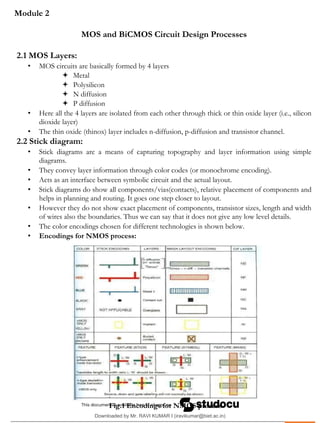
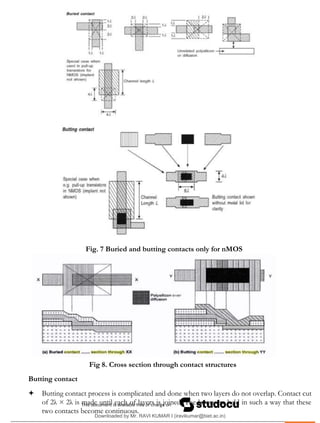
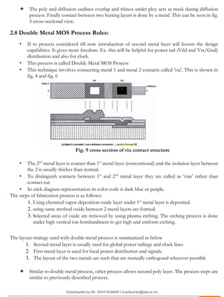
This document discusses MOS and BiCMOS circuit design processes. It describes the layers used in MOS circuits and provides color encodings for stick diagrams. Stick diagrams capture layer information through simple diagrams and act as an interface between symbolic circuits and layouts. The document outlines the NMOS and CMOS design processes, including rules for drawing stick diagrams and placing transistors. It also covers design rules and lambda-based rules for layout dimensions and separations. Contact cuts and buried contacts are discussed for making electrical connections between layers.


![.
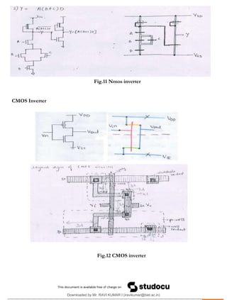
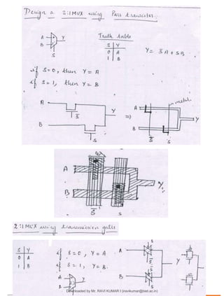
Procedure to draw Stick Diagram:
1) Draw two metal lines/ power rails providing sufficient space to accommodate all transistors. i.e:
Vdd & Vss.
2) Draw demarcation line in the middle of the two power lines.
3) Draw P+ diffusion above demarcation and N+ diffusion below demarcation
4) Draw polysilicon to represent Pmos and Nmos which represents gates of the transistor.
5) Connect source terminal of transistors to supply.
6) Drain terminals of transistor are connected using metal 1.
7) Place contact cuts wherever necessary.
8) Draw X which represents substrate and P-well contact on power lines.
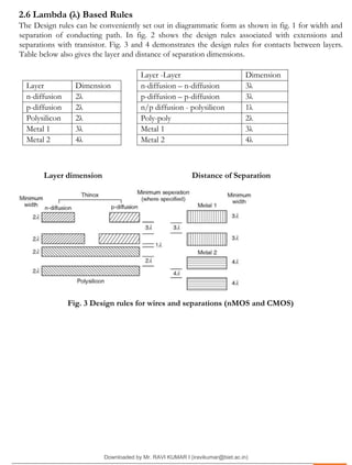
2.5 DESIGN RULES AND LAYOUTS
Layout: describes actual layers and geometry on silicon substrate to implement a function
(Expressions).
[Diffusion region where transistor can be formed is called active region, polysilicon serves as the gate
of MOS transistor. L defines channel length and W represents width of channel/active region]
Design rules: are set of guidelines which specify minimum dimension and spacing allowed in layout
drawing. Design rules also acts a communication link between circuit designers and process engineers
during manufacturing phase.
Goal of design rule: is to achieve optimum yield. Yield = (No. of good chips on wafer)/(Total no. of
chips on wafer).
Design rules are also called layout rules. If the circuit performance has to be increased then rules must
be more aggressive. Else this leads to non-function of the circuit or yield reduction.
There are two rules.
1. Micron Rule - Absolute Dimension rule, here all sizes and spacing are specified in micron. Here
the circuit density is the important goal.
2. Lambda (λ) Based Rules - The Lambda based design rules are proposed by Mead and Conway.
Scalable design rules, here this design rule normalizes all geometric design rule by parameter lambda
(λ) also called as scaling factor/feature size. In this all mask patterns are expressed as multiples of
lambda.
Advantages of lambda based design rules:
1. The mask layout can be scaled down proportionally if the feature size of the fabrication process is
reduced.
2. Design rules are conservative.
3. This rule enable technology changes and design reuse and reduced design cost.
Disadvantages:
1. Linear scaling cannot be extended and is limited over range of dimension (1-3 μm)
2. As rules are conservative, results in over dimension and density of design is less.
Downloaded by Mr. RAVI KUMAR I (iravikumar@biet.ac.in)
lOMoARcPSD|3283145](https://image.slidesharecdn.com/module-2-mos-and-bi-cmos-circuit-design-process-230405144406-17168d75/85/VLSI-Design2-4-320.jpg)


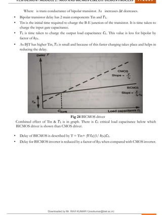
![VLSI DESIGN| MODULE 2 : MOS AND BICMOS CIRCUIT DESIGN PROCESS 1 7 E C 6 3
M I T M Y S O R E | D E P T . O F E L E C T R O N I C S & C O M M U N I C A T I O N E N G G . 30
For N even, total delay = τ = 2.5 𝑓 τ (nmos) or
τ = 3.5 𝑓 τ (cmos)
In all cases, delay ἀ N
• Total delay is minimized If 𝑓 assumes the value e. i.e: each stage is approximately 2.7
times wider than its predecessor and it is applicable for both cmos and nmos inverters.
Thus assuming 𝑓 = 𝑒, we have
Number of stages N= ln(𝑦)
And overall delay 𝑡𝑑
N even: 𝑡𝑑= 2.5 N τ (NMOS) or 𝑡𝑑= 3.5 N τ (CMOS)
N odd: 𝑡𝑑= [2.5 (N-1)+1]e τ (NMOS) or 𝑡𝑑= [3.5 (N-1)+1]e τ (CMOS) For
ΔVin which indicates logic 0 to 1 transistion of Vin.
𝑡𝑑= [2.5 (N-1)+4]e τ (NMOS) or 𝑡𝑑= [3.5 (N-1)+5]e τ (CMOS) For
ΔVin which indicates logic 1 to 0 transistion of Vin.
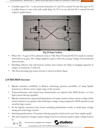
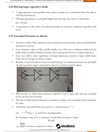
2.18 Super buffers
• Asymmetry of conventional inverter gives rise to significant delay problems when used to
drive large capacitive loads.
Common approach used in nmos inverter is to use super buffers an inverting type nmos super
buffer is shown in figure.
Fig 23. nmos super buffer
Downloaded by Mr. RAVI KUMAR I (iravikumar@biet.ac.in)
lOMoARcPSD|3283145](https://image.slidesharecdn.com/module-2-mos-and-bi-cmos-circuit-design-process-230405144406-17168d75/85/VLSI-Design2-31-320.jpg)