CONTENTS:
❑Static CMOS Design
▪Complementary logic
▪ Rationed Logic
▪ Pass Transistor Logic
❑Dynamic CMOS Design
▪ Basic Principles
▪ Speed power dissipation
▪ Issues in dynamic design
▪ Cascading Dynamic Gates
▪ Latches Vs Registers.
▪ Latch based design
▪ Instability and meta stability
▪ Multiplexer based latches.
3.
Static CMOS Design
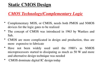
CMOSTechnology/Complementary Logic
• Complementary MOS, or CMOS, needs both PMOS and NMOS
devices for the logic gates to be realized
• The concept of CMOS was introduced in 1963 by Wanlass and
Sah.
• CMOS are more complicated in design and production, thus are
more expensive to fabricate
• Have not been widely used until the 1980’s as NMOS
microprocessors started to dissipating as much as 50 W and more
and alternative design technique was needed
• CMOS dominate digital IC design today
4.
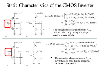
Static Characteristics ofthe CMOS Inverter
• The capacitor discharges through RonN ,
current exists only during discharge,
no dc current exists.
• The capacitor charges through RonP ,
current exists only during charging,
no dc current exists.
5.
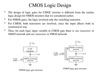
CMOS Logic Design
•The design of logic gates for CMOC inverter is different from the similar
logic design for NMOS inverters that we considered earlier.
• For NMOS gates, the logic involved only the switching transistor.
• For CMOS, both transistors are involved, since the input affects both in
symmetrical way.
• Thus, for each logic input variable in CMOS gate there is one transistor in
NMOS network and one transistor in PMOS network.
CMOS logic gate structure
NMOS logic gate structure
Load
transistor
6.
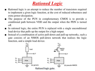
Rationed Logic
▪ Rationedlogic is an attempt to reduce the number of transistors required
to implement a given logic function, at the cost of reduced robustness and
extra power dissipation.
▪ The purpose of the PUN in complementary CMOS is to provide a
conditional path between VDD and the output when the PDN is turned
off.
▪ In rationed logic, the entire PUN is replaced with a single unconditional
load device that pulls up the output for a high output.
▪ Instead of a combination of active pull-down and pull-up networks, such a
gate consists of an NMOS pull-down network that realizes the logic
function, and a simple load device.
8.
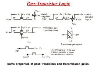
Pass-Transistor Logic
▪ Inelectronics, Pass Transistor Logic describes several logic
families used in the design of integrated circuits.
▪ It reduces the count of transistors used to make different logic
gates, by eliminating redundant transistors.
▪ Transistors are used as switches to pass logic levels between nodes
of a circuit, instead of as switches connected directly to supply
voltage
▪ Switches and switch logic may be formed from simple n- or p-
pass transistors or from transmission gates (complementary
switches) comprising an n-pass and a p-pass transistor in parallel
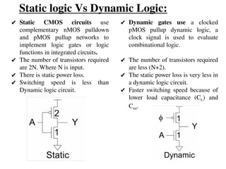
Static logic VsDynamic Logic:
✔ Static CMOS circuits use
complementary nMOS pulldown
and pMOS pullup networks to
implement logic gates or logic
functions in integrated circuits.
✔ The number of transistors required
are 2N. Where N is input.
✔ There is static power loss.
✔ Switching speed is less than
Dynamic logic circuit.
✔ Dynamic gates use a clocked
pMOS pullup dynamic logic, a
clock signal is used to evaluate
combinational logic.
✔ The number of transistors required
are less (N+2).
✔ The static power loss is very less in
a dynamic logic circuit.
✔ Faster switching speed because of
lower load capacitance (CL) and
Cint.
11.
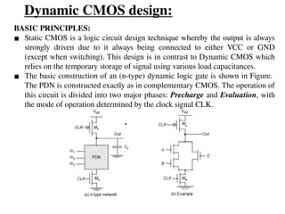
Dynamic CMOS design:
BASICPRINCIPLES:
▪ Static CMOS is a logic circuit design technique whereby the output is always
strongly driven due to it always being connected to either VCC or GND
(except when switching). This design is in contrast to Dynamic CMOS which
relies on the temporary storage of signal using various load capacitances.
▪ The basic construction of an (n-type) dynamic logic gate is shown in Figure.
The PDN is constructed exactly as in complementary CMOS. The operation of
this circuit is divided into two major phases: Precharge and Evaluation, with
the mode of operation determined by the clock signal CLK.
12.
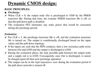
Dynamic CMOS design:
BASICPRINCIPLES:
▪ Precharge:
✔ When CLK = 0, the output node Out is precharged to VDD by the PMOS
transistor Mp. During that time, the evaluate NMOS transistor Me is off, so
that the pull-down path is disabled.
✔ The evaluation FET eliminates any static power that would be consumed
during the precharge period.
Evaluation:
✔ For CLK = 1, the precharge transistor Mp is off, and the evaluation transistor
Me is turned on. The output is conditionally discharged based on the input
values and the pull-down topology.
✔ If the inputs are such that the PDN conducts, then a low resistance path exists
between Out and GND and the output is discharged to GND.
✔ During the evaluation phase, the only possible path between the output node
and a supply rail is to GND. Consequently, once Out is discharged, it cannot
be charged again till then next precharge operation.
✔ The output can be in the high-impedance state during the evaluation period if
the pull-down network is turned off.
13.
Dynamic CMOS design:
SPEEDAND POWER DISSIPATION OF DYNAMIC LOGIC:
POWER DISSIPATION:
✔ In today's world, we need sleeker devices with more capabilities
and longer battery life. This can be achieved by packing more
components on smaller chips
✔ Power dissipation occurs in all the circuits that are currently used,
which increases the overall power consumption, making it less
suitable for mobile applications which need longer battery life.
✔ The power consumption is also considered as an important
criterion in VLSI design along with timing and area.
✔ Power dissipation has become one of the major problem as it
results in heating up of the device which will affects the operation
of a chip.
14.
Dynamic CMOS design:
SPEEDAND POWER DISSIPATION OF DYNAMIC LOGIC:
POWER DISSIPATION-
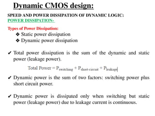
Types of Power Dissipation:
❖ Static power dissipation
❖ Dynamic power dissipation
✔ Total power dissipation is the sum of the dynamic and static
power (leakage power).
✔ Dynamic power is the sum of two factors: switching power plus
short circuit power.
✔ Dynamic power is dissipated only when switching but static
power (leakage power) due to leakage current is continuous.
15.
Dynamic CMOS design:
SPEEDAND POWER DISSIPATION OF DYNAMIC LOGIC:
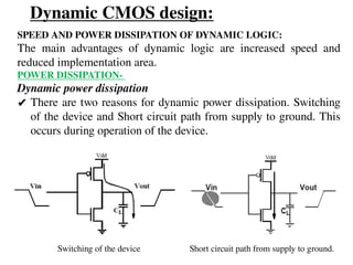
The main advantages of dynamic logic are increased speed and
reduced implementation area.
POWER DISSIPATION-
Dynamic power dissipation
✔ There are two reasons for dynamic power dissipation. Switching
of the device and Short circuit path from supply to ground. This
occurs during operation of the device.
Switching of the device Short circuit path from supply to ground.
16.
Dynamic CMOS design:
SPEEDAND POWER DISSIPATION OF DYNAMIC LOGIC:
POWER DISSIPATION- Dynamic power dissipation
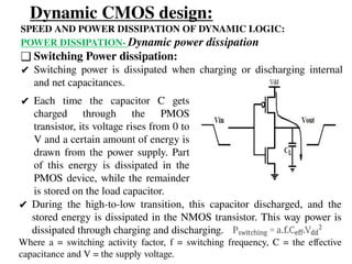
❑ Switching Power dissipation:
✔ Switching power is dissipated when charging or discharging internal
and net capacitances.
✔ Each time the capacitor C gets
charged through the PMOS
transistor, its voltage rises from 0 to
V and a certain amount of energy is
drawn from the power supply. Part
of this energy is dissipated in the
PMOS device, while the remainder
is stored on the load capacitor.
✔ During the high-to-low transition, this capacitor discharged, and the
stored energy is dissipated in the NMOS transistor. This way power is
dissipated through charging and discharging.
Where a = switching activity factor, f = switching frequency, C = the effective
capacitance and V = the supply voltage.
17.
Dynamic CMOS design:
SPEEDAND POWER DISSIPATION OF DYNAMIC LOGIC:
POWER DISSIPATION- Dynamic power dissipation
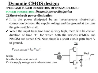
❑ Short-circuit power dissipation:
✔ It is the power dissipated by an instantaneous short-circuit
connection between the supply voltage and the ground at the time
the gate switches state.
✔ When the input transition time is very high, there will be certain
duration of time “t”, for which both the devices (PMOS and
NMOS) are turned ON. Now, there is a short circuit path from V
to ground.
Where
Isc= the short circuit current,
V= the supply voltage and t =short circuit time.
18.
Dynamic CMOS design:
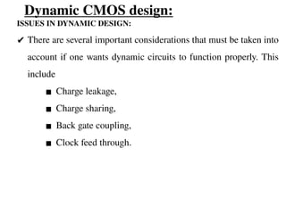
ISSUESIN DYNAMIC DESIGN:
✔ There are several important considerations that must be taken into
account if one wants dynamic circuits to function properly. This
include
▪ Charge leakage,
▪ Charge sharing,
▪ Back gate coupling,
▪ Clock feed through.
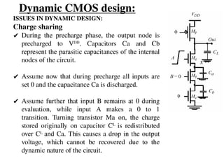
Dynamic CMOS design:
ISSUESIN DYNAMIC DESIGN:
Charge sharing
✔ During the precharge phase, the output node is
precharged to VDD
. Capacitors Ca and Cb
represent the parasitic capacitances of the internal
nodes of the circuit.
✔ Assume now that during precharge all inputs are
set 0 and the capacitance Ca is discharged.
✔ Assume further that input B remains at 0 during
evaluation, while input A makes a 0 to 1
transition. Turning transistor Ma on, the charge
stored originally on capacitor CL
is redistributed
over CL
and Ca. This causes a drop in the output
voltage, which cannot be recovered due to the
dynamic nature of the circuit.
21.
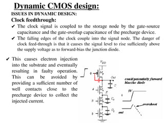
Dynamic CMOS design:
ISSUESIN DYNAMIC DESIGN:
Clock feedthrough:
✔ The clock signal is coupled to the storage node by the gate-source
capacitance and the gate-overlap capacitance of the precharge device.
✔ The falling edges of the clock couple into the signal node. The danger of
clock feed-through is that it causes the signal level to rise sufficiently above
the supply voltage as to forward-bias the junction diode.
✔ This causes electron injection
into the substrate and eventually
resulting in faulty operation.
This can be avoided by
providing a sufficient number of
well contacts close to the
precharge device to collect the
injected current.
22.
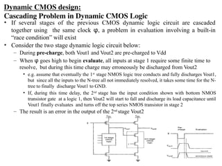
Dynamic CMOS design:
CascadingProblem in Dynamic CMOS Logic
• If several stages of the previous CMOS dynamic logic circuit are cascaded
together using the same clock φ, a problem in evaluation involving a built-in
“race condition” will exist
• Consider the two stage dynamic logic circuit below:
– During pre-charge, both Vout1 and Vout2 are pre-charged to Vdd
– When φ goes high to begin evaluate, all inputs at stage 1 require some finite time to
resolve, but during this time charge may erroneously be discharged from Vout2
• e.g. assume that eventually the 1st
stage NMOS logic tree conducts and fully discharges Vout1,
but since all the inputs to the N-tree all not immediately resolved, it takes some time for the N-
tree to finally discharge Vout1 to GND.
• If, during this time delay, the 2nd
stage has the input condition shown with bottom NMOS
transistor gate at a logic 1, then Vout2 will start to fall and discharge its load capacitance until
Vout1 finally evaluates and turns off the top series NMOS transistor in stage 2
– The result is an error in the output of the 2nd
stage Vout2
23.
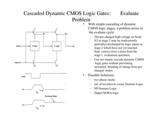
Cascaded Dynamic CMOSLogic Gates: Evaluate
Problem
• With simple cascading of dynamic
CMOS logic stages, a problem arises in
the evaluate cycle:
– The pre-charged high voltage on Node
N2 in stage 2 may be inadvertently
(partially) discharged by logic inputs to
stage 2 which have not yet reached
final correct (low) values from the
stage 1 evaluation operation.
– Can not simply cascade dynamic CMOS
logic gates without preventing
unwanted bleeding of charge from pre-
charged nodes
• Possible Solutions:
– two phase clocks
– use of inverters to create Domino Logic
– NP Domino Logic
– Zipper/NORA logic
24.
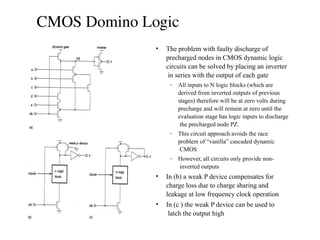
CMOS Domino Logic
•The problem with faulty discharge of
precharged nodes in CMOS dynamic logic
circuits can be solved by placing an inverter
in series with the output of each gate
– All inputs to N logic blocks (which are
derived from inverted outputs of previous
stages) therefore will be at zero volts during
precharge and will remain at zero until the
evaluation stage has logic inputs to discharge
the precharged node PZ.
– This circuit approach avoids the race
problem of “vanilla” cascaded dynamic
CMOS
– However, all circuits only provide non-
inverted outputs
• In (b) a weak P device compensates for
charge loss due to charge sharing and
leakage at low frequency clock operation
• In (c ) the weak P device can be used to
latch the output high
25.
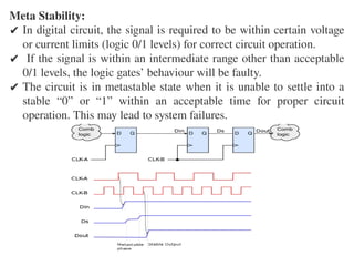
Meta Stability:
✔ Indigital circuit, the signal is required to be within certain voltage
or current limits (logic 0/1 levels) for correct circuit operation.
✔ If the signal is within an intermediate range other than acceptable
0/1 levels, the logic gates’ behaviour will be faulty.
✔ The circuit is in metastable state when it is unable to settle into a
stable “0” or “1” within an acceptable time for proper circuit
operation. This may lead to system failures.
26.
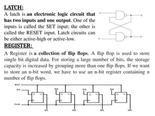
LATCH:
A latch isan electronic logic circuit that
has two inputs and one output. One of the
inputs is called the SET input; the other is
called the RESET input. Latch circuits can
be either active-high or active-low.
REGISTER:
A Register is a collection of flip flops. A flip flop is used to store
single bit digital data. For storing a large number of bits, the storage
capacity is increased by grouping more than one flip flops. If we want
to store an n-bit word, we have to use an n-bit register containing n
number of flip flops.
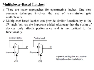
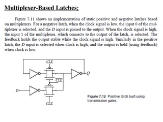
Multiplexer-Based Latches:
✔ Thereare many approaches for constructing latches. One very
common technique involves the use of transmission gate
multiplexers.
✔ Multiplexer based latches can provide similar functionality to the
SR latch, but has the important added advantage that the sizing of
devices only affects performance and is not critical to the
functionality