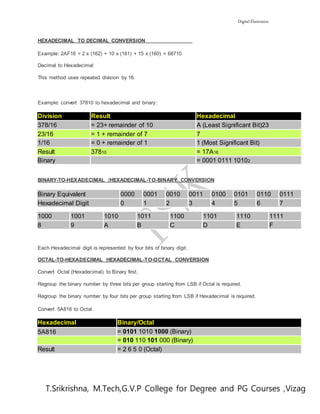
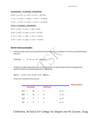
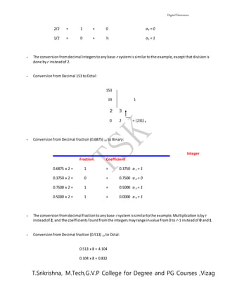
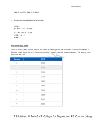
Downloaded 261 times


![Digital Electronics
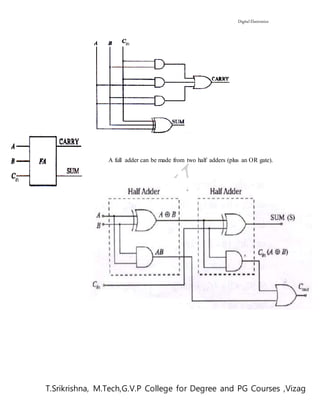
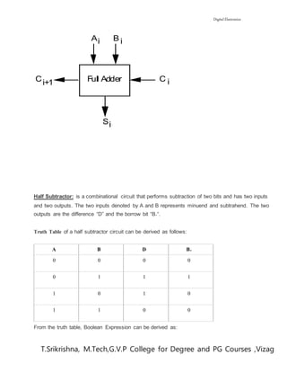
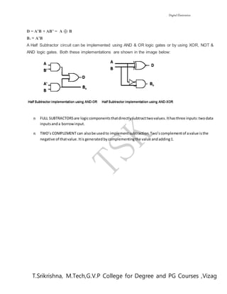
T.Srikrishna, M.Tech,G.V.P College for Degree and PG Courses ,Vizag
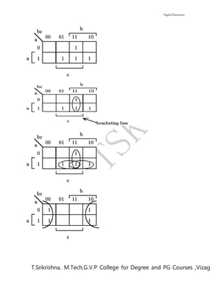
3. Translate eachgroup intoa product termby eliminatinganyvariable whose value changesfromcell tocell.
4. Sumall the productterms.
Note: Don't care conditionscanbe usedto provide furthersimplificationof the representationof afunction.
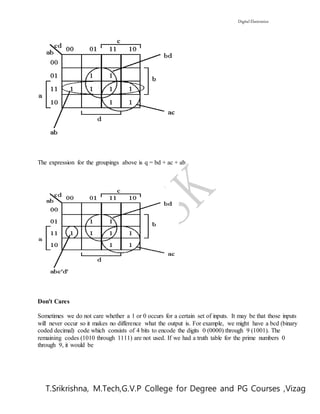
Given the following truth table for the function m:
The Boolean algebraic expression is
m = a'bc + ab'c + abc' + abc.
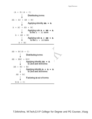
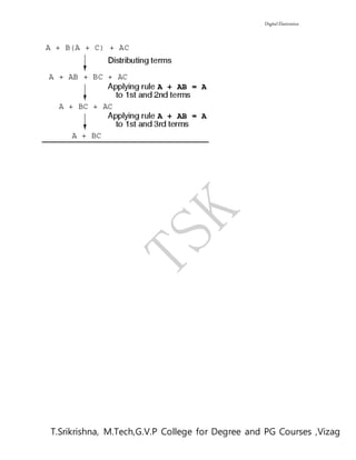
We have seen that the minimization is done as follows.
m = a'bc + abc + ab'c + abc + abc' + abc
= (a' + a)bc + a(b' + b)c + ab(c' + c) ]:[ aaNB
= bc + ac + ab
The abc term was replicated and combined with the other terms.
To use a Karnaugh map we draw the following map which has a position (square) corresponding to each
of the 8 possible combinations of the 3 Boolean variables. The upper left position corresponds to the 000
row of the truth table, the lower right position corresponds to 110. Each square has two coordinates, the
vertical coordinate corresponds to the value of variable a and the horizontal corresponds to the values of b
and c.](https://image.slidesharecdn.com/de1-170203105825/85/Digital-Electronics-Notes-32-320.jpg)

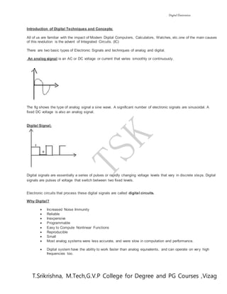
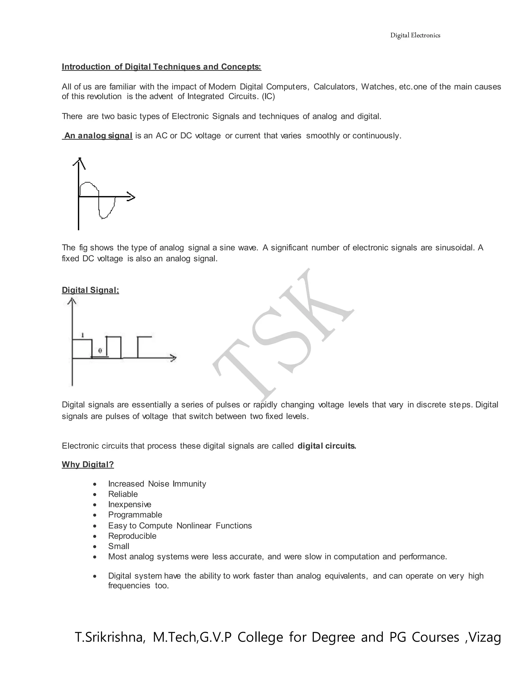
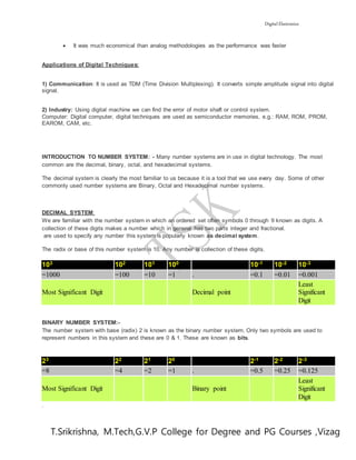
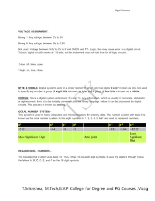
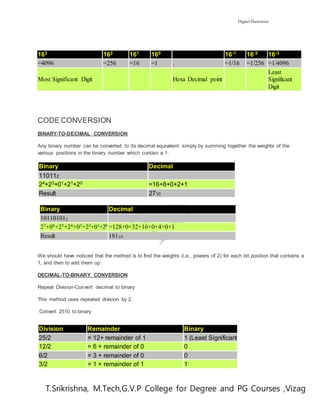
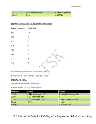
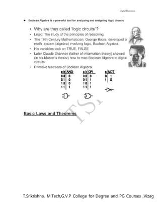
This document provides an introduction to digital electronics and digital signals. It discusses the basics of analog and digital signals, with digital signals taking on discrete voltage levels compared to the continuous variation of analog signals. The advantages of digital techniques are explained, such as increased noise immunity and reliability. Common number systems are introduced, including binary, octal, hexadecimal and decimal, along with methods for converting between them. The key concepts of bytes, coding and voltage assignments in digital circuits are also covered at a high level.