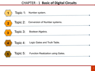
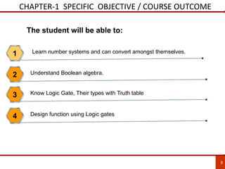
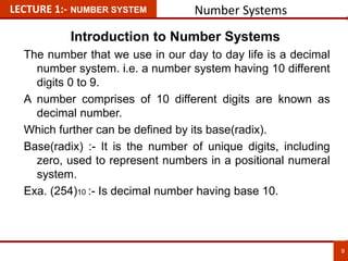
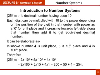
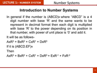
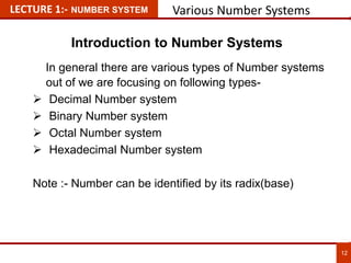
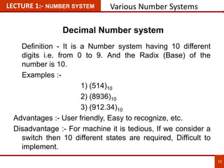
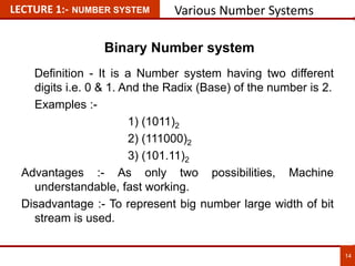
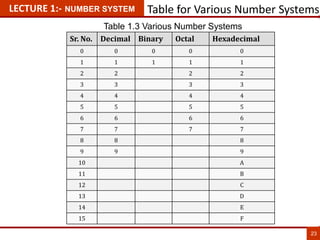
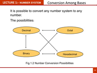
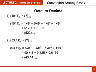
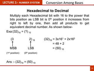
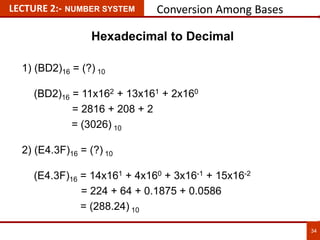
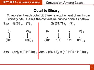
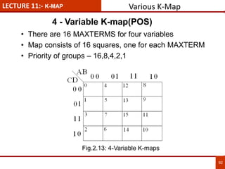
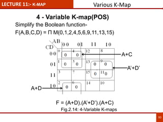
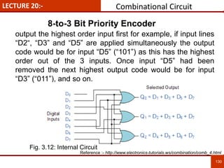
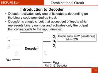
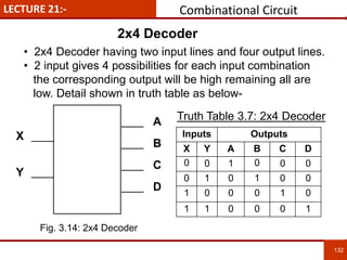
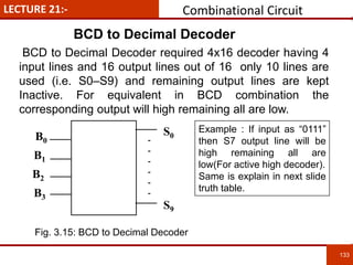
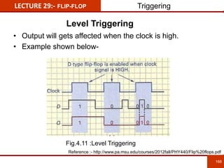
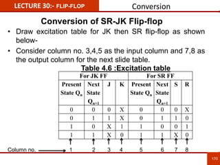
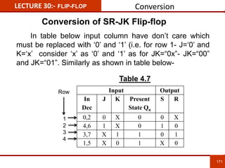
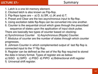
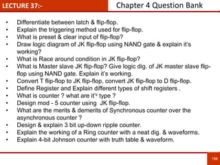
1. The document discusses various number systems including decimal, binary, octal, and hexadecimal. It provides details on how to convert between these different number systems.
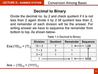
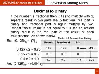
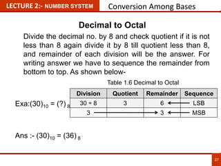
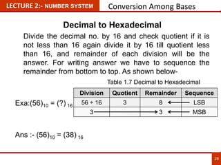
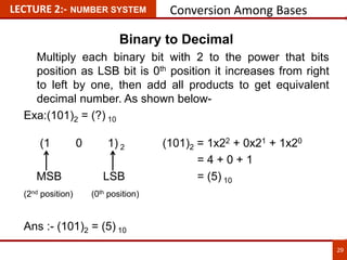
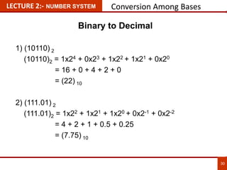
2. Conversion methods between number systems are explained, such as dividing decimal numbers by powers of 2, 8, or 16 to get the binary, octal, or hexadecimal representation respectively.
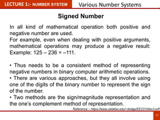
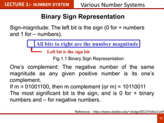
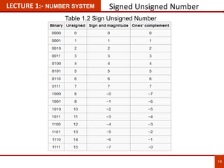
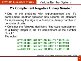
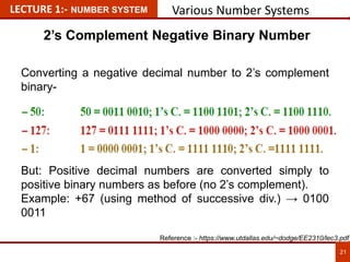
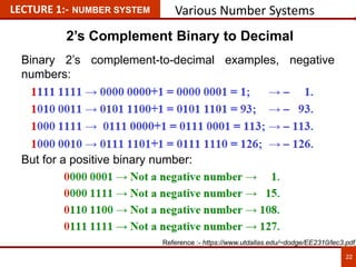
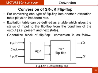
3. Signed number representation is also covered, explaining sign-magnitude, one's complement, and two's complement methods.