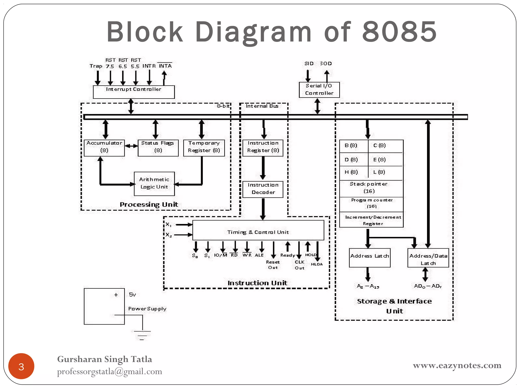
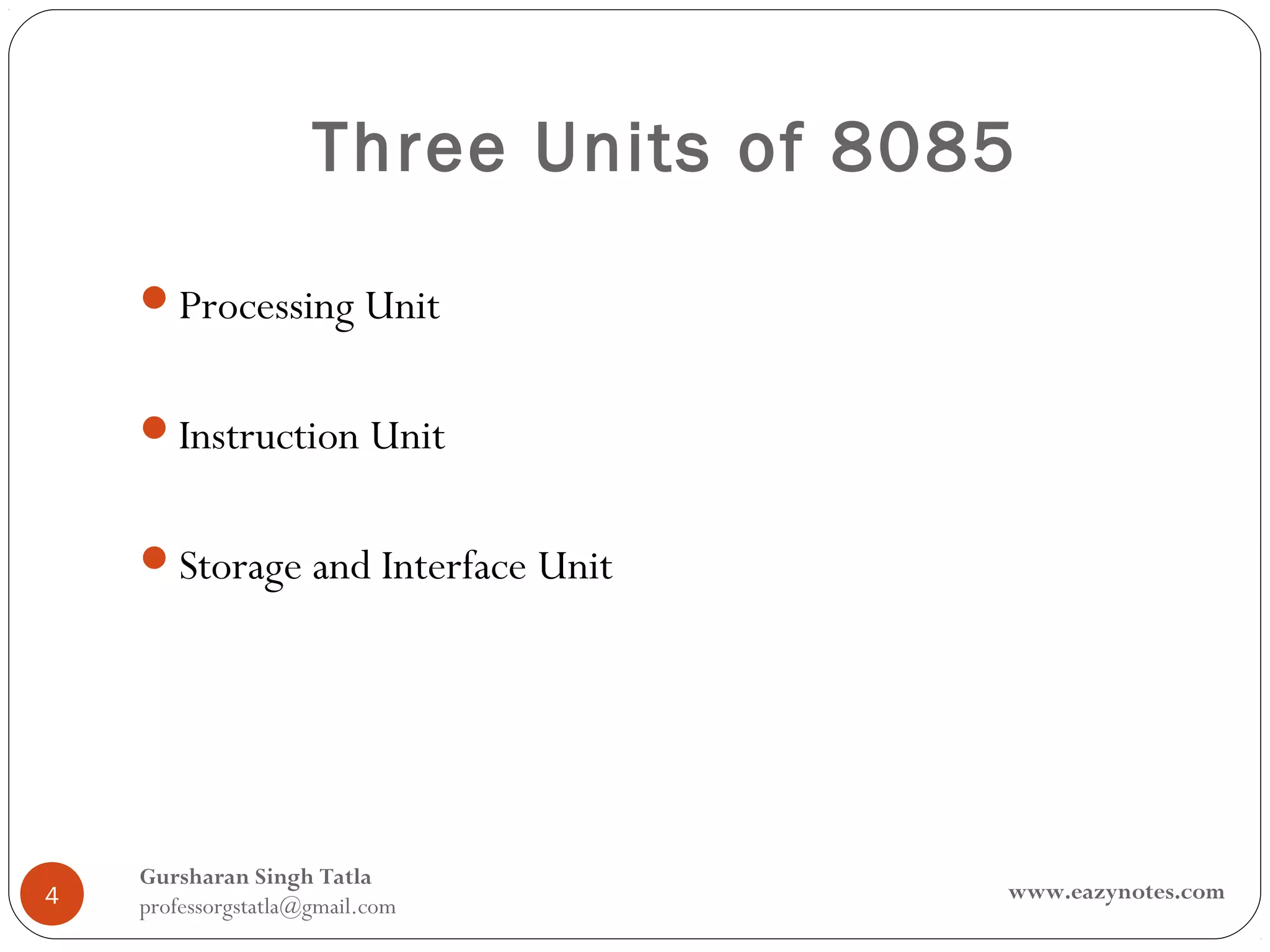
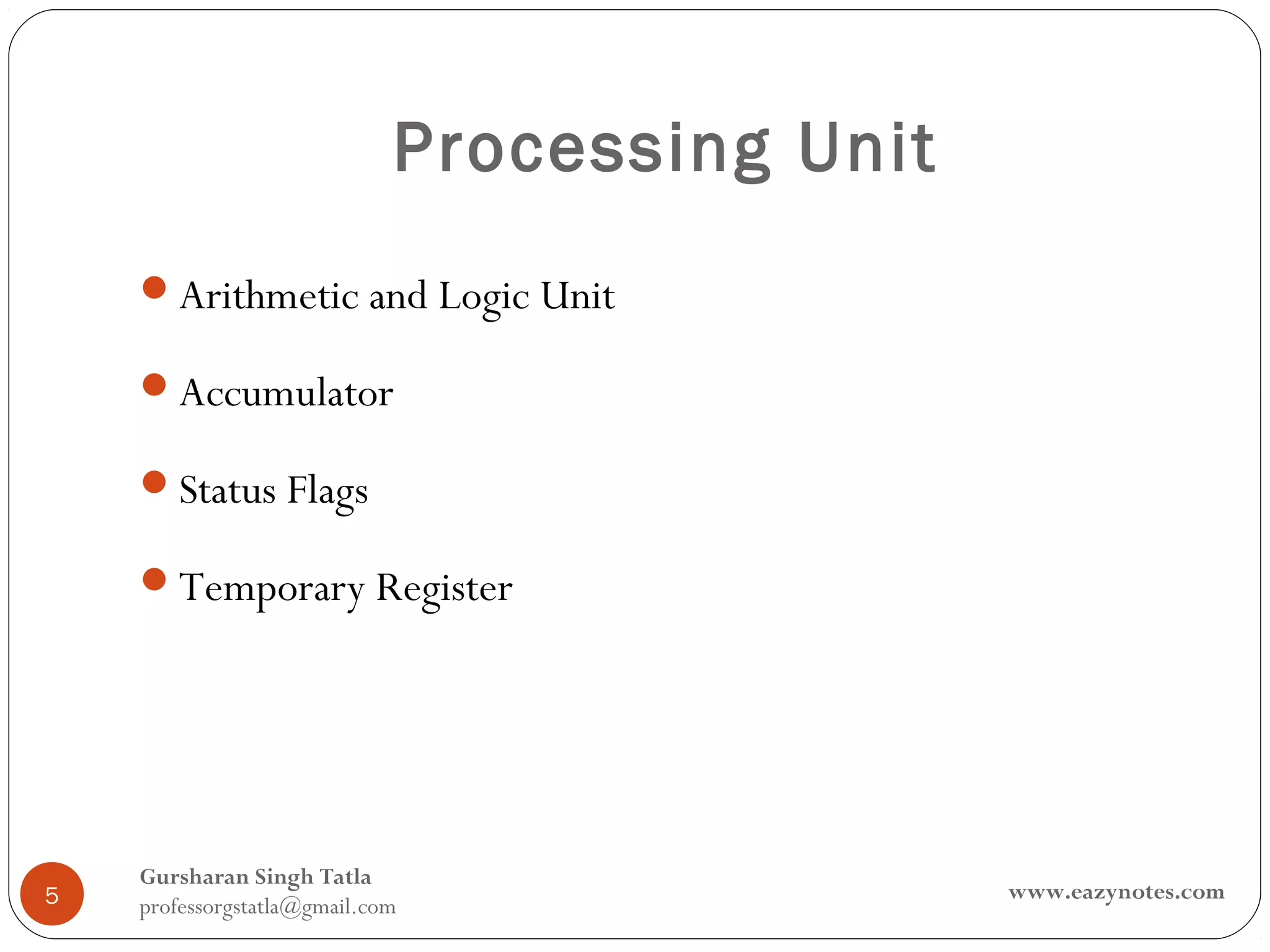
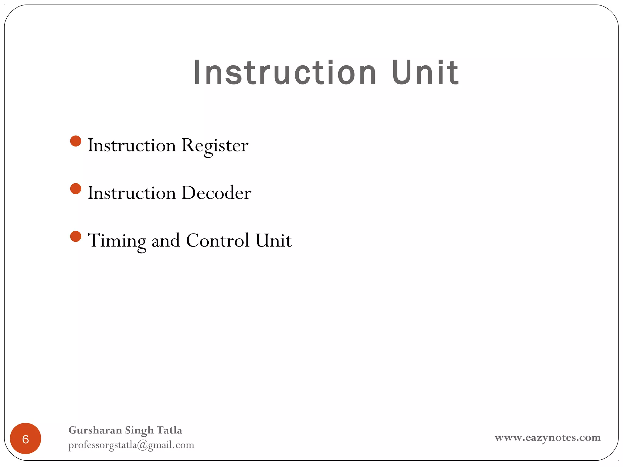
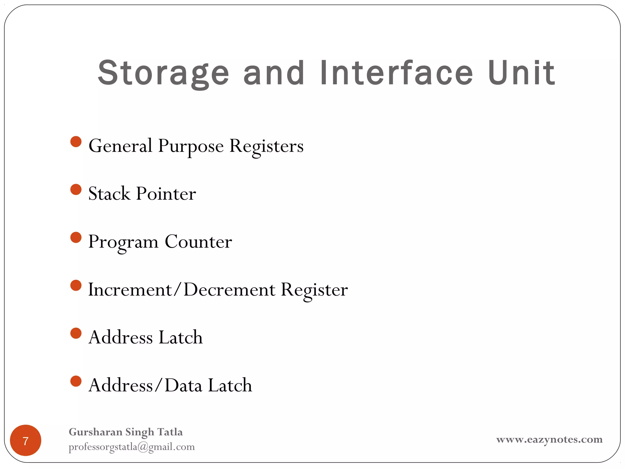
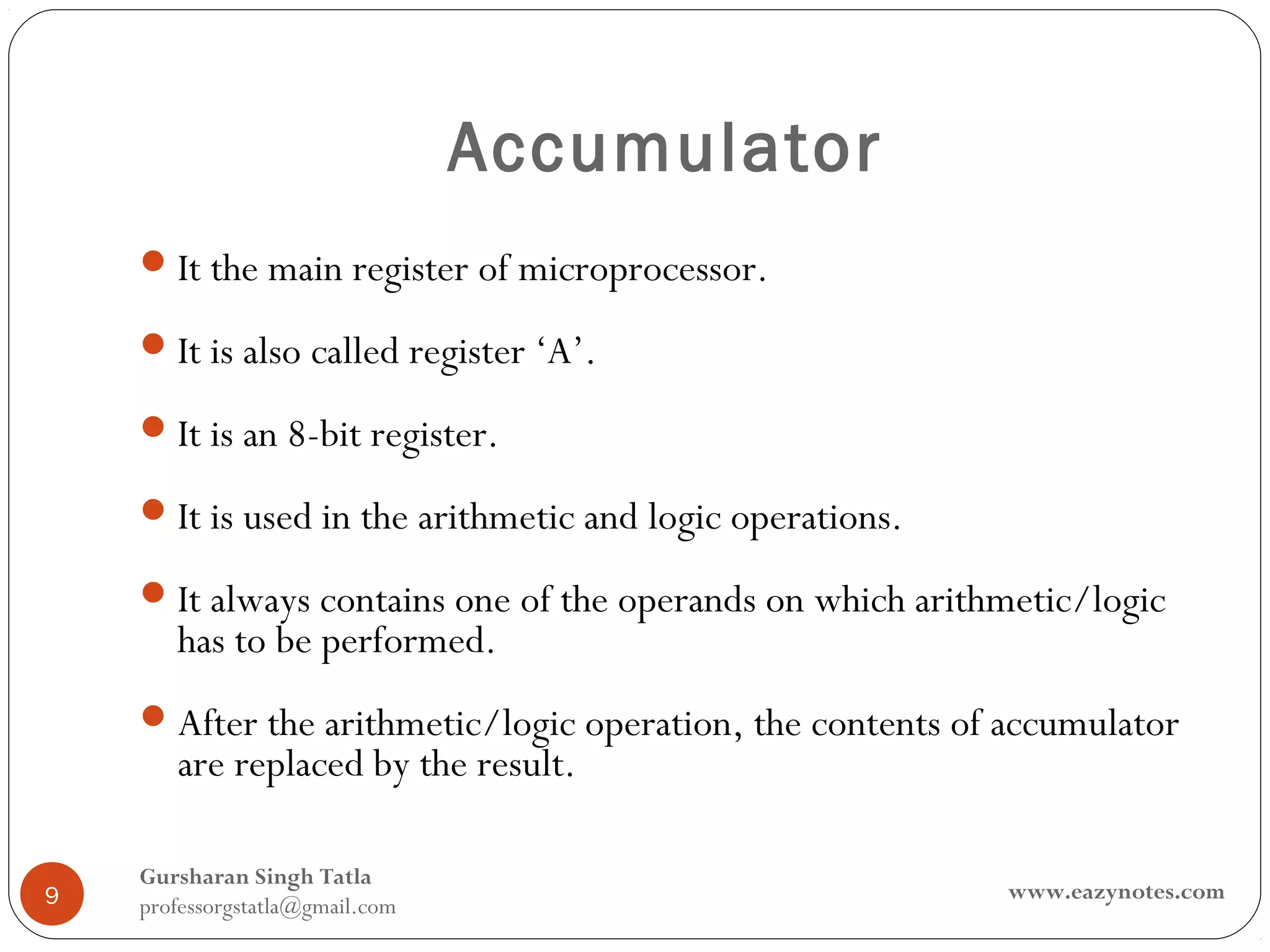
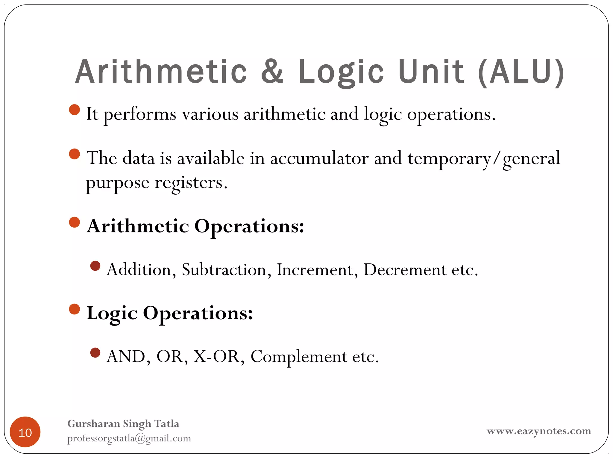
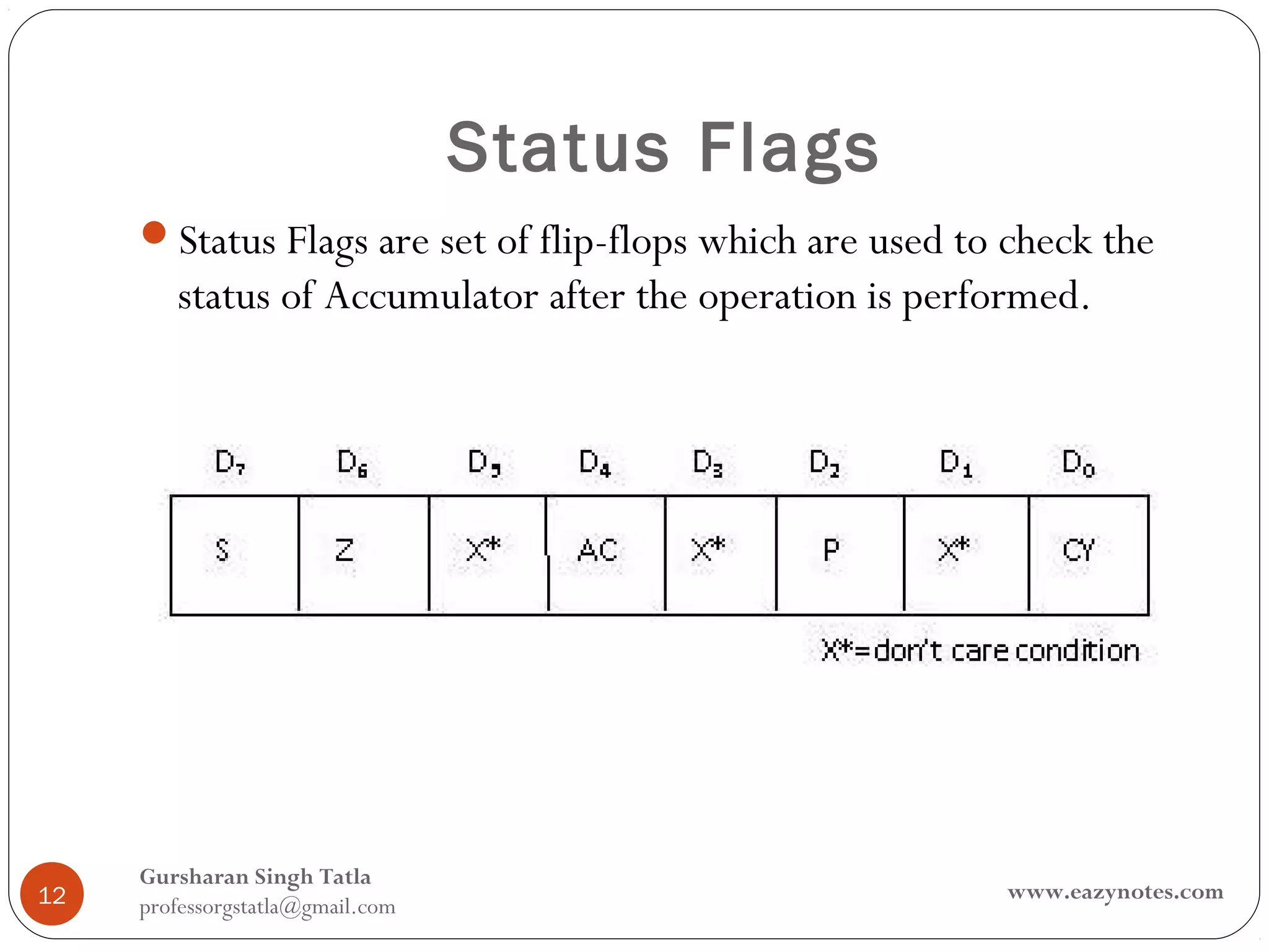
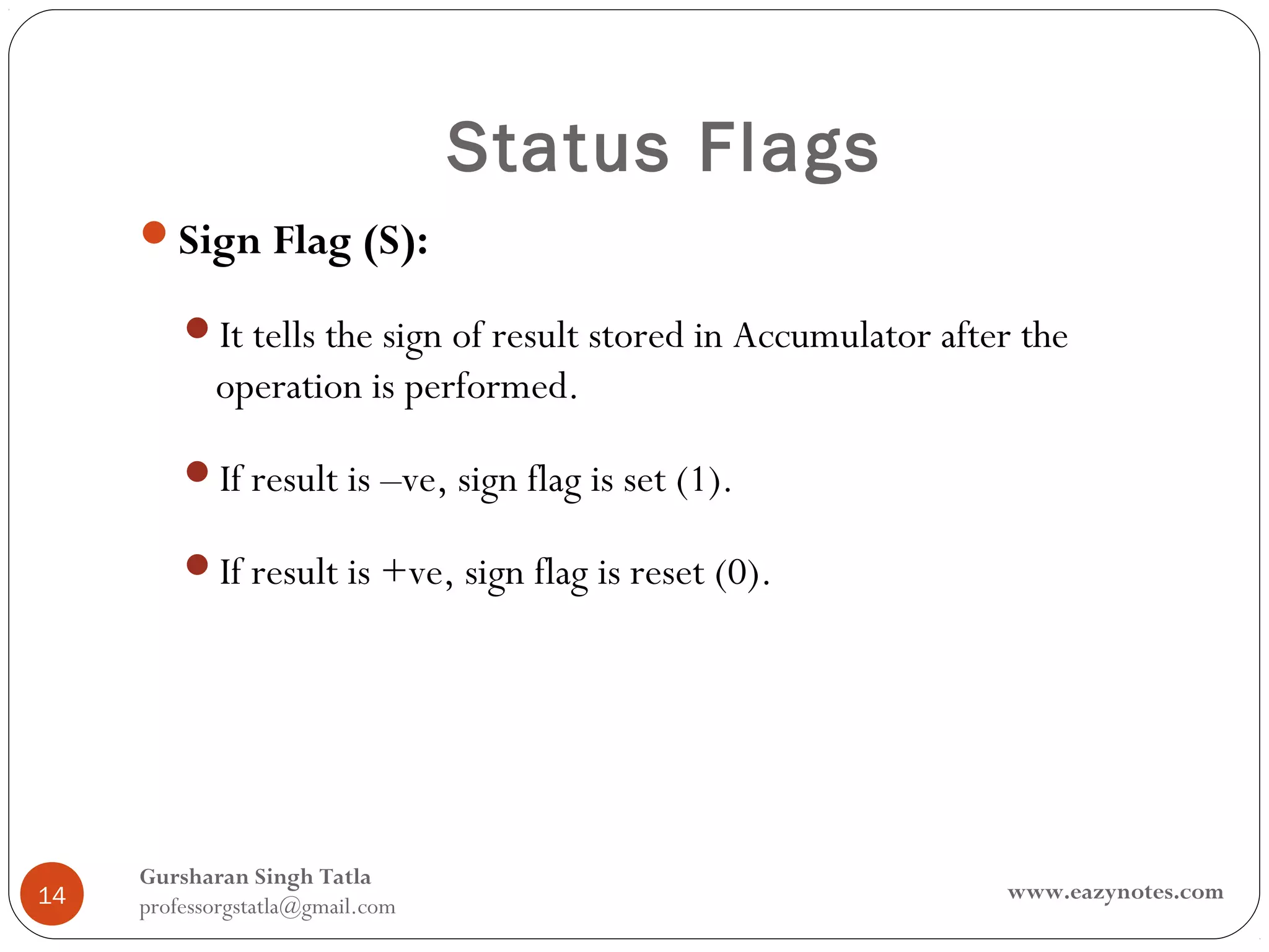
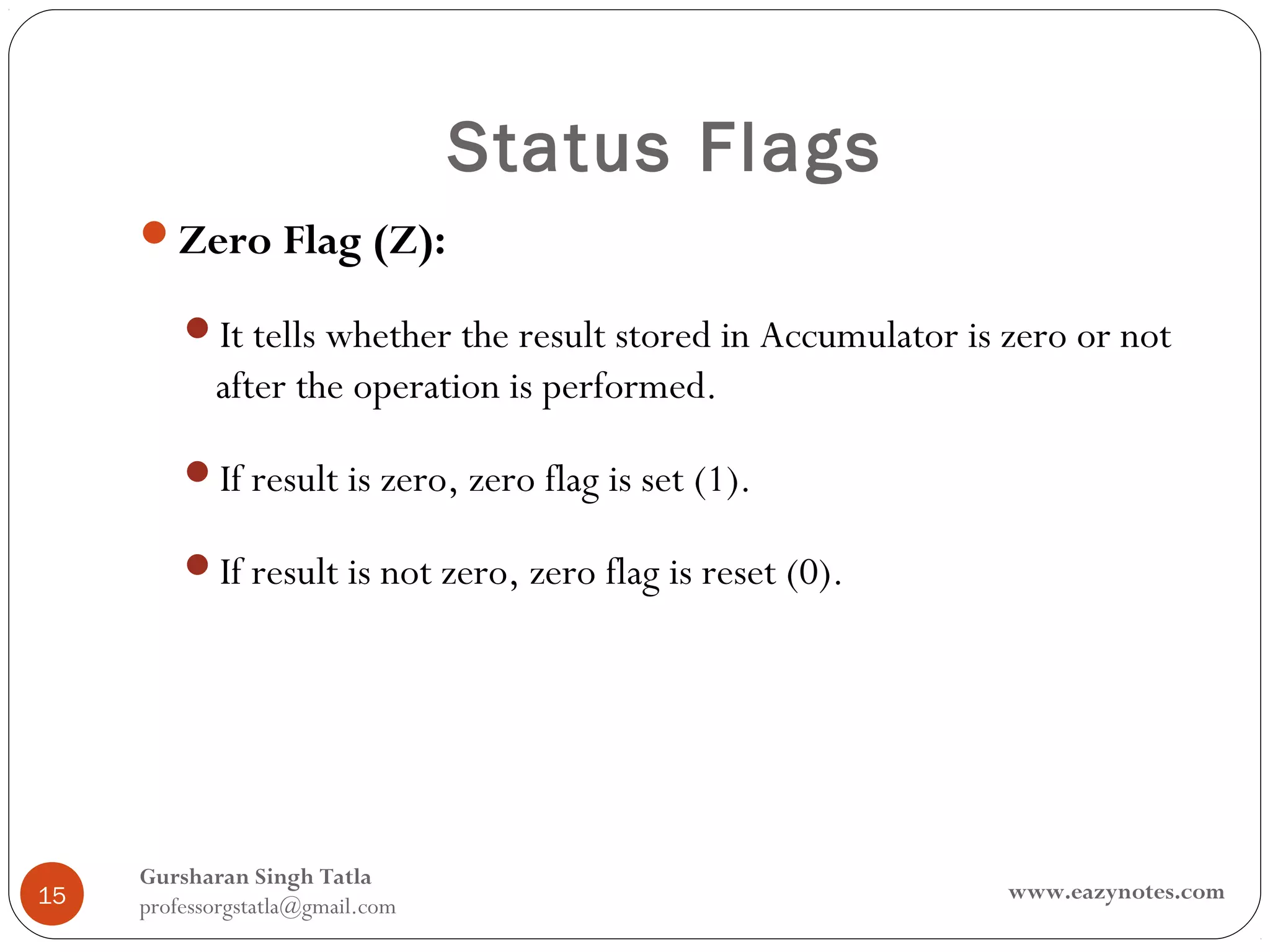
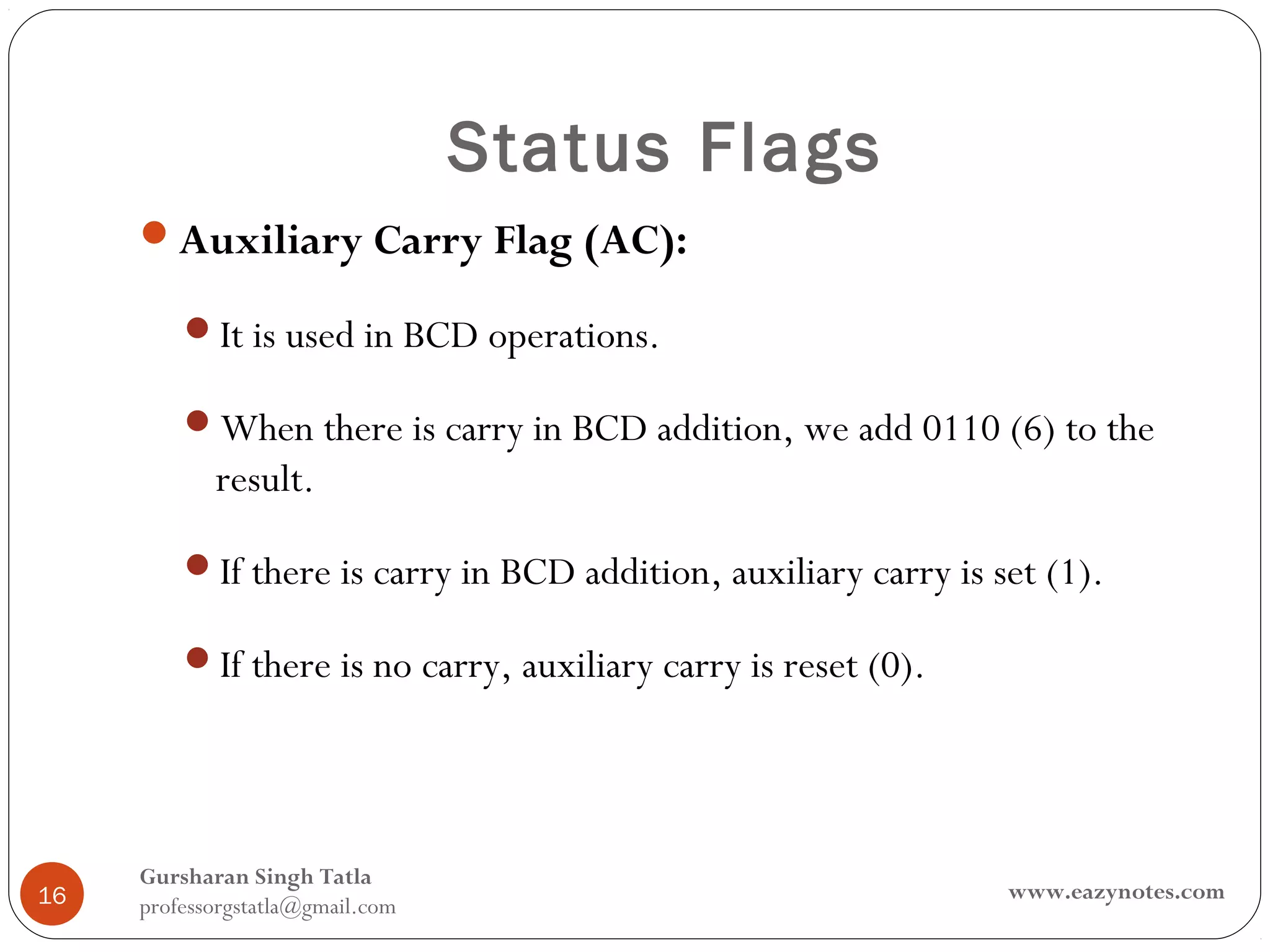
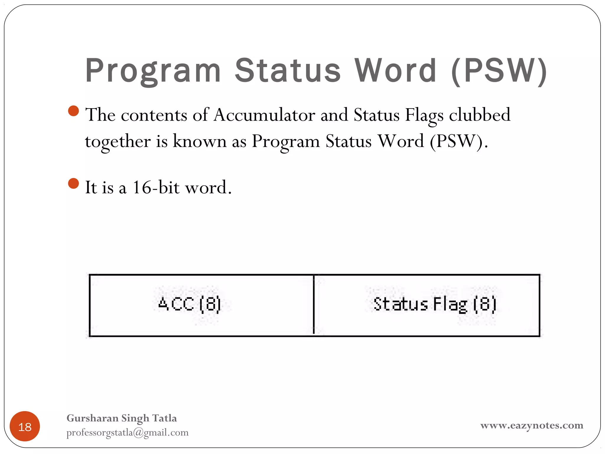
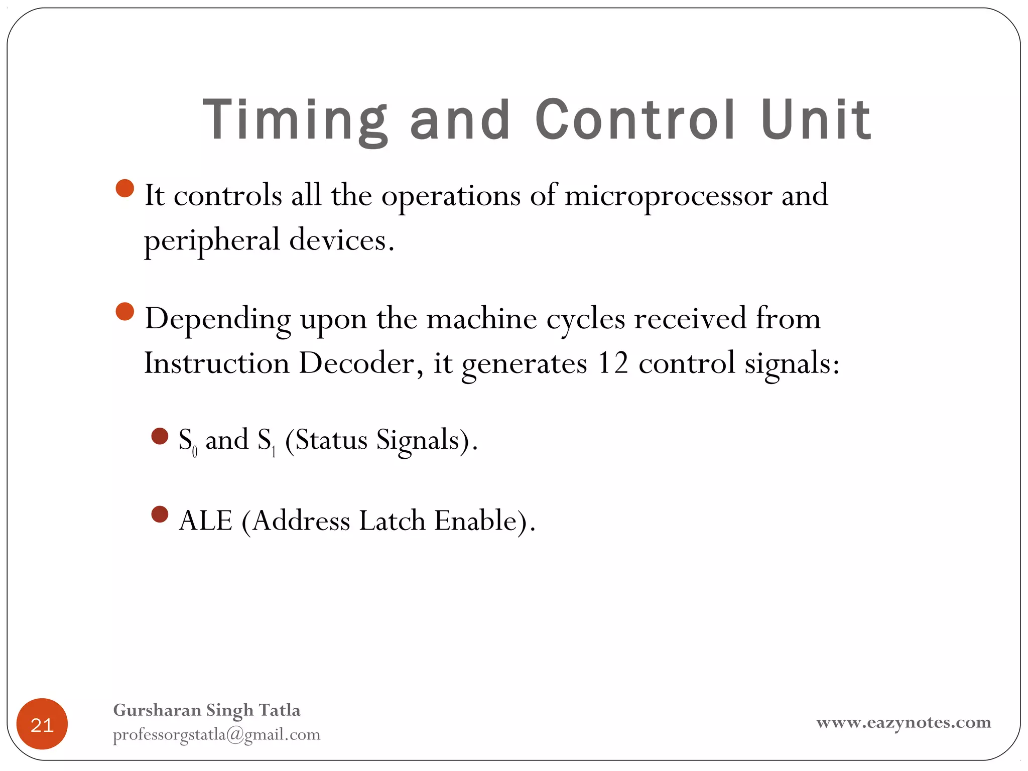
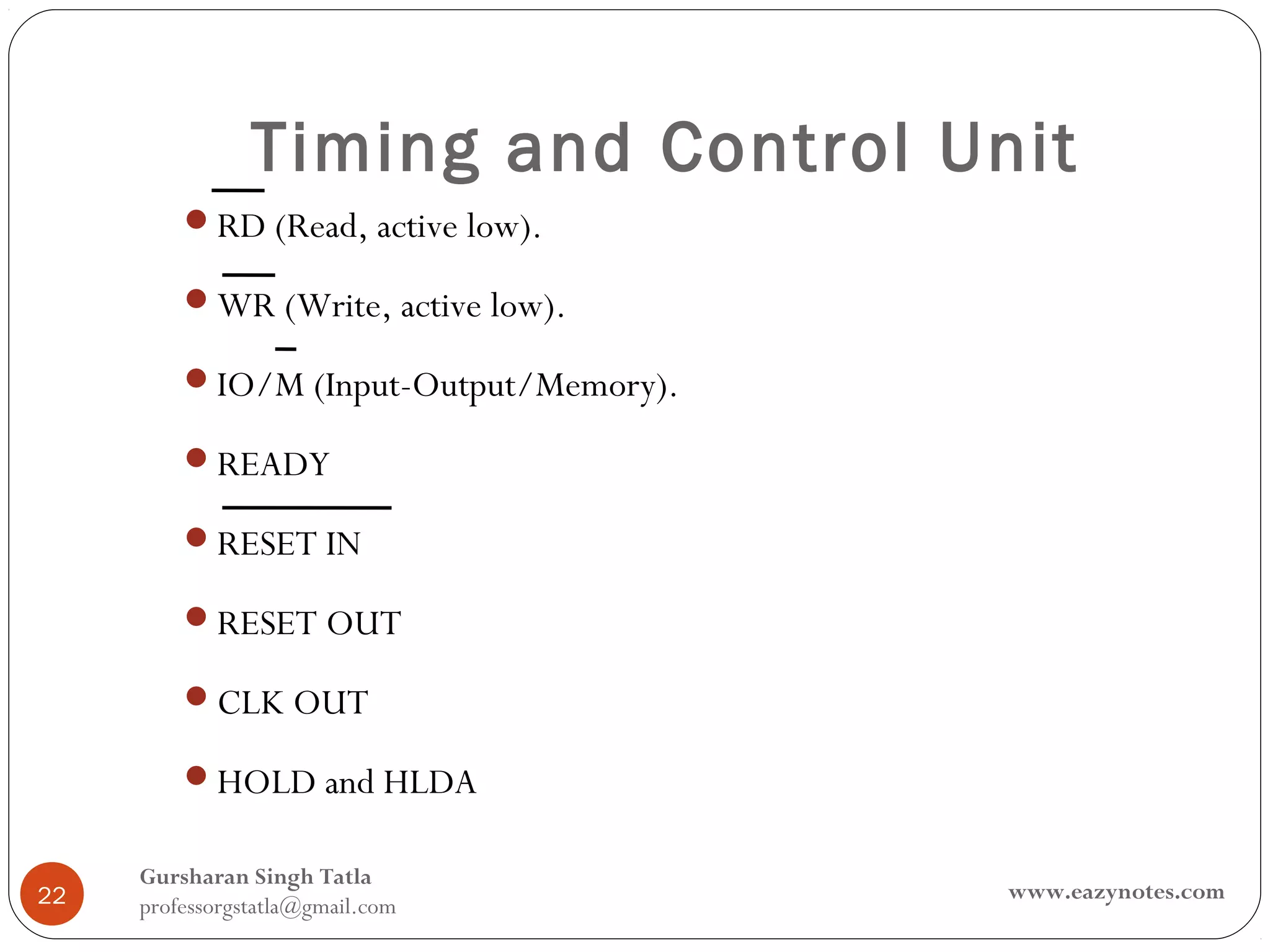
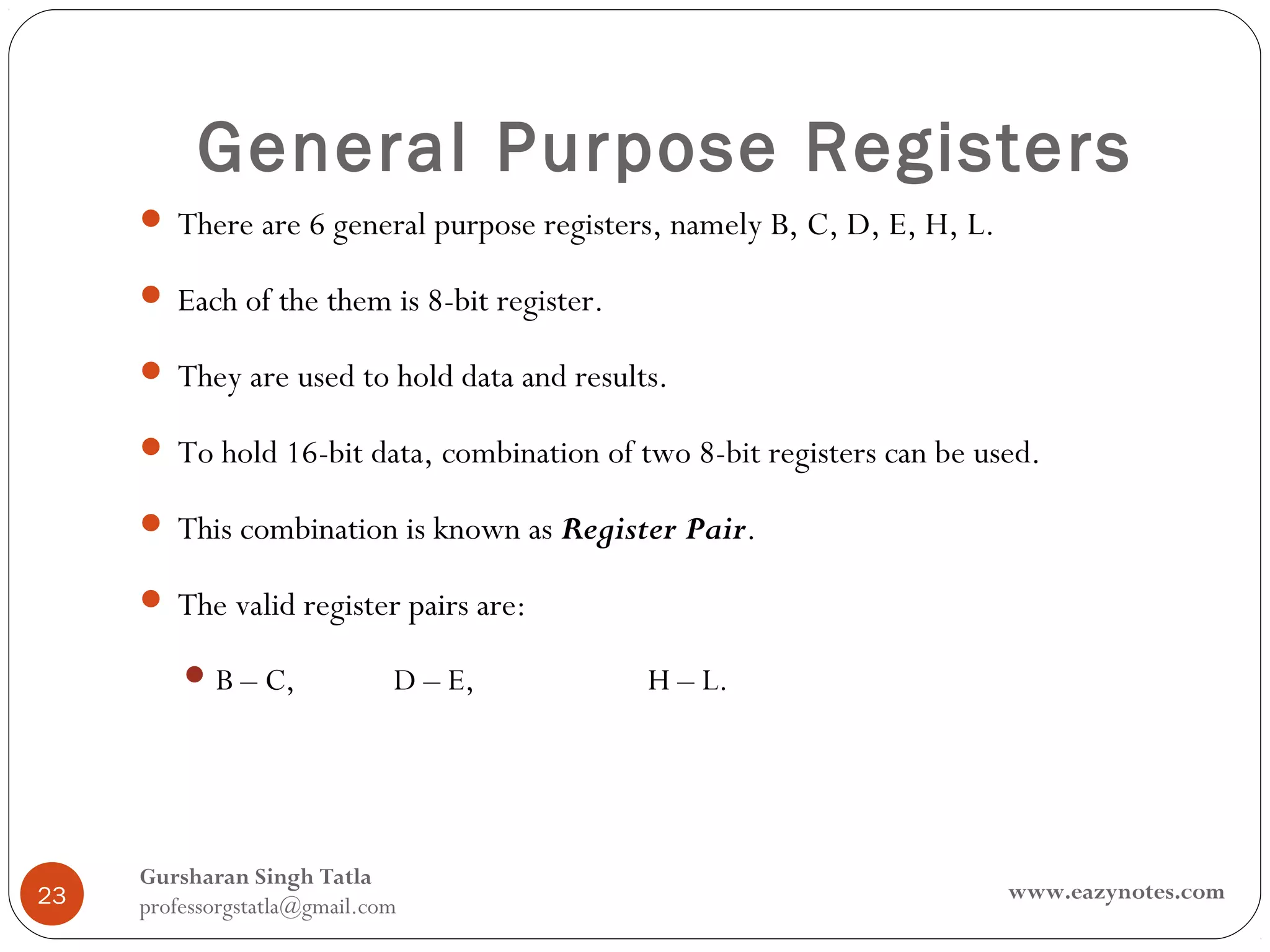
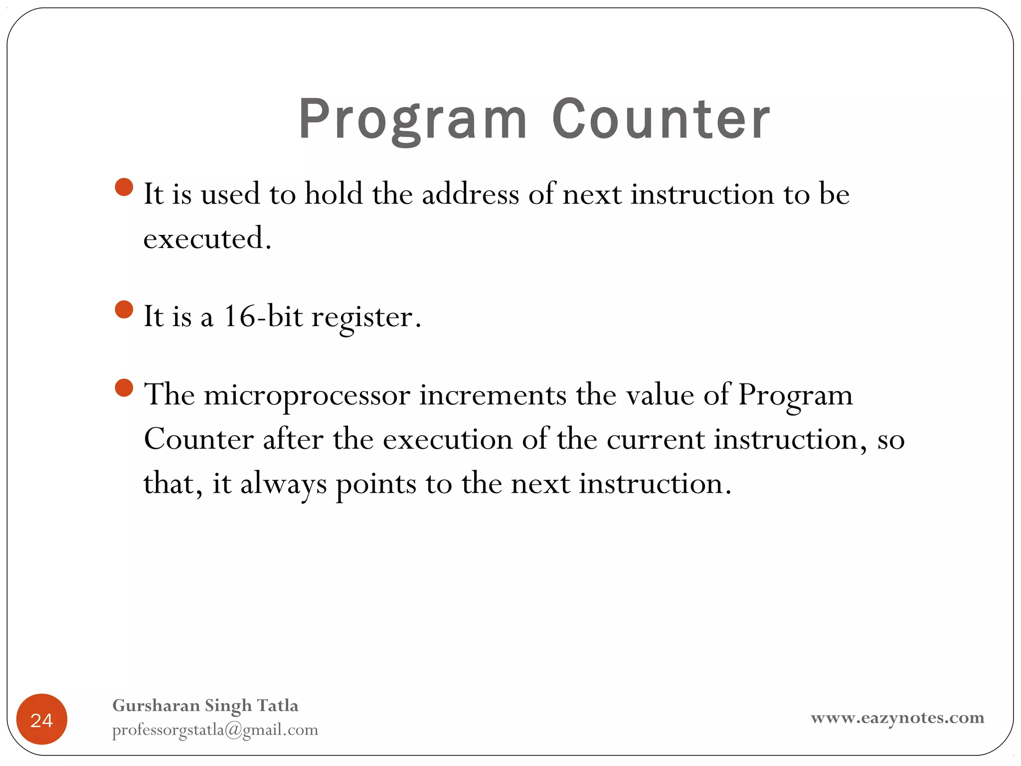
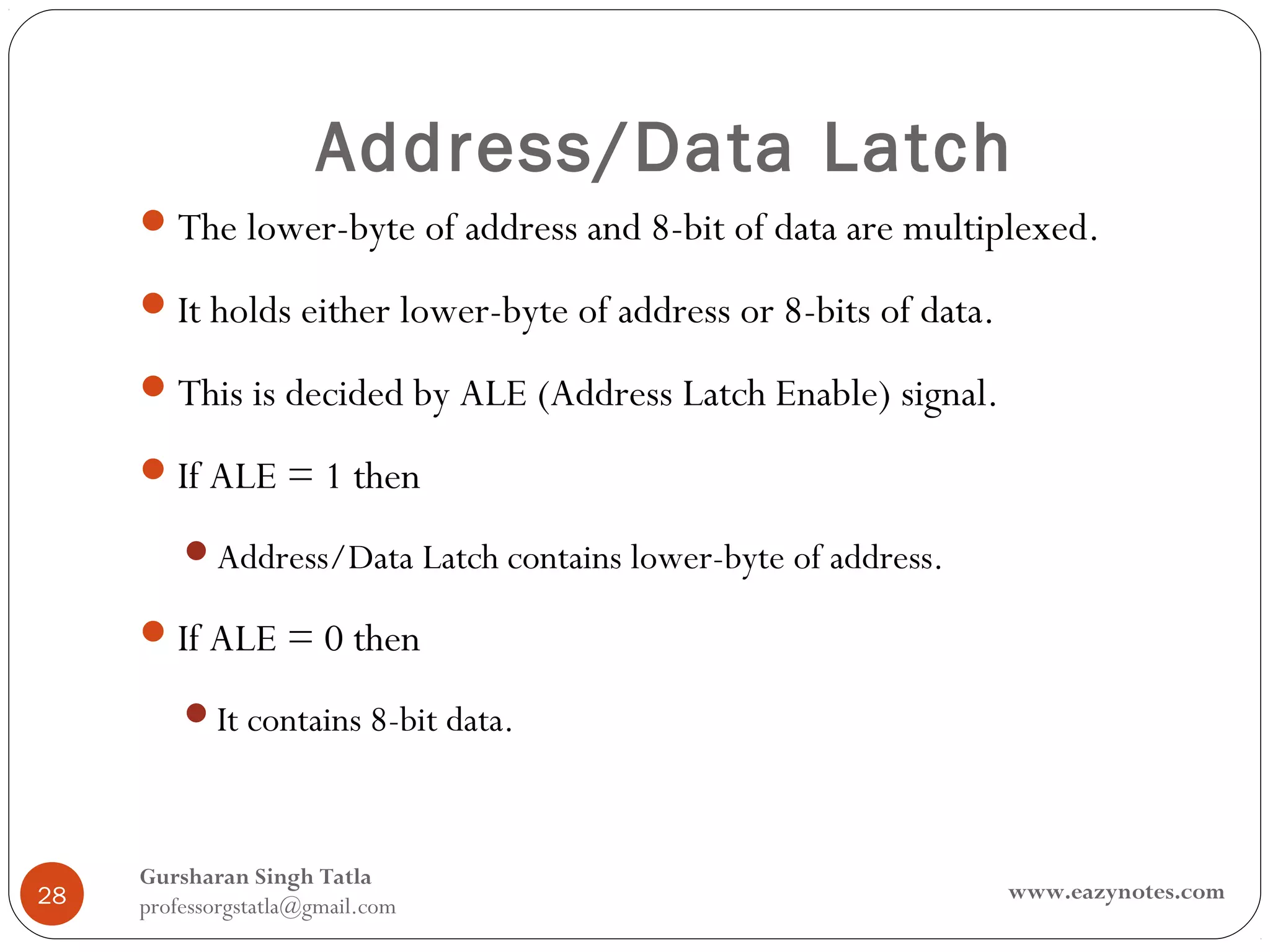
The document describes the architecture and components of the Intel 8085 microprocessor. It discusses the three main units: the processing unit containing the ALU, accumulator, and status flags; the instruction unit containing the instruction register, decoder, and timing/control unit; and the storage and interface unit containing the registers, program counter, stack pointer, and address/data latches. It provides details on the functions of the accumulator, ALU, status flags, instruction register, and other individual components.
The 8155 and 8156 microprocessor interface chips differ in that the 8155 has an active low Chip Enable (CE) signal, while the 8156 has an active high CE signal. The 8155 is a multifunction chip that contains RAM, I/O ports, and a timer. It has two 8-bit I/O ports, one 6-bit I/O port, a 14-bit counter/timer, 2Kb of RAM, and can be interfaced with the 8085 microprocessor. The document then provides details on the pinout, memory mapping, control register, port configurations, timer operation modes, and status register of the 8155 chip.
The document discusses interrupts in microprocessors. It defines an interrupt as a process where an external device can get the microprocessor's attention. There are two main methods for communication between I/O devices and microprocessors - polling and interrupts. The interrupt method is more efficient as it allows the microprocessor to immediately service interrupt requests from devices rather than wasting time polling each one. Interrupts can be software-triggered using instructions or hardware-triggered by external signals. The 8085 microprocessor supports vectored and non-vectored interrupts of varying priorities that allow interrupt service routines to be executed in response to interrupt requests.
8085 MICROPROCESSOR ARCHITECTURE AND ITS OPERATIONSRamaPrabha24
This document discusses the architecture and operations of microprocessors. It focuses on the Intel 8085 microprocessor. The 8085 architecture consists of a register array, ALU and logic group, instruction decoder and encoder, interrupt control group, and serial I/O control group. The register array contains general purpose registers, temporary registers, special purpose registers like the accumulator, flags register, and instruction register, and 16-bit registers like the program counter and stack pointer. The ALU performs arithmetic and logical operations. The instruction decoder decodes instructions and the timing and control circuitry manages the sequencing of operations. Microprocessor operations include memory reads/writes, I/O reads/writes using address, data and control buses, internal data operations
The 8051 microcontroller has 128 bytes of internal RAM and 4Kbytes of internal ROM memory. It uses the same addresses for code and data but accesses the correct memory based on whether an operation is for code or data. The 128 bytes of internal RAM are organized into 4 banks of 32 bytes each. External memory can be added if more memory is needed for program code or variable data storage. The document also provides information on interfacing external program and data memory with the 8051 microcontroller.
The document discusses interrupts in computers. It defines interrupts as events external to the currently executing process that cause process suspension so it can be resumed later. Interrupts allow I/O devices to get CPU attention asynchronously. The document contrasts interrupt handling with polling and describes hardware/software, masked/non-masked, and vectored/non-vectored interrupt types. It also explains interrupt processing, including interrupt acknowledgement and use of interrupt vectors and tables.
The document discusses the architecture of the 8085 microprocessor. It describes the main components of a processor system including the CPU, ALU, registers, memory and I/O interfaces. It then provides details on the internal architecture of the 8085 CPU, describing its registers including the program counter, accumulator, flags register and stack pointer. It also explains the address bus, data bus and control bus and how the 8085 uses time-sharing of address/data lines.
The document discusses the 8051 microcontroller, including its architecture, pin configuration, memory organization, timers, interrupts, and interfacing capabilities. It describes the 8051's features like on-chip RAM, ROM, timers and low power consumption which make it suitable for control applications. The document outlines the differences between microprocessors and microcontrollers, and covers various interfacing examples like switches, LEDs, 7-segment displays, LCDs, ADCs and relay interfacing. It concludes with common applications of the 8051 such as in automobiles, industrial processing, robotics and consumer electronics.
The document provides an overview of microprocessors and the 8085 microprocessor architecture. It discusses that a microprocessor is a programmable VLSI chip that includes an ALU, registers, and control circuits. The 8085 is an 8-bit microprocessor that can address 64KB of memory. It has three main functional blocks - a register array, ALU and logical group, and instruction decoder/timing and control circuitry. The document also describes the various registers, buses, pins and control signals of the 8085 microprocessor.
This document discusses different types of semiconductor memory used in computing systems. It describes volatile memory like static RAM (SRAM) and dynamic RAM (DRAM), as well as non-volatile memory such as ROM, MRAM, and flash memory. The basic unit of semiconductor memory is the memory cell, which can store a single bit using MOS or CMOS fabrication. Memory architectures are organized in arrays or hierarchies to store large amounts of data within computer systems.
This document discusses memory and I/O interfacing with the 8085 microprocessor. It defines interfaces as points of interaction between components that allow communication. Memory interfacing requires address decoding and multiplexing of address and data lines. I/O devices can be interfaced either through memory mapping or I/O mapping. Common memory types include RAM, ROM, SRAM and DRAM. RAM can be static or dynamic. ROM includes PROM, EPROM and EEPROM. A stack is a reserved part of memory used to temporarily store information during program execution.
The document describes the Intel 8086 microprocessor, which was launched in 1978 as the first 16-bit microprocessor. It had major improvements over the 8085 microprocessor, with higher execution speeds. The 8086 had a 16-bit data bus, 20-bit address bus, and could address up to 1MB of memory. It included features like multiplication and division support. The document provides detailed information on the various pins and signals of the 8086 microprocessor.
The document discusses the evolution of microprocessors from 1971 to present. It begins with Intel releasing the first microprocessor, the 4-bit 4004, in 1971. The document then outlines the progression from 4-bit to 8-bit to 16-bit and finally 32-bit and 64-bit microprocessors. It provides details on the features of early microprocessors like the 8008, 8080, 8085 and later models like the 8086, 80286, 80386 and Pentium. The number of transistors integrated onto a single chip doubled every 18 months, as predicted by Moore's Law.
The document discusses microprocessors, microcontrollers, and the 8085 microprocessor. It defines a microprocessor as a programmable device that performs arithmetic and logical operations on numbers according to a stored program. A microcontroller is similar but has memory and I/O functions integrated on a single chip. The 8085 is an 8-bit microprocessor with 40 pins that can address 64KB of memory and has 74 instructions across 5 addressing modes. It uses multiplexed address and data lines to reduce pins.
The document discusses the architecture of the Intel 8085 microprocessor. It describes the 8085 as an 8-bit microprocessor introduced in 1976 that uses a single +5 volt power supply. The internal architecture includes a control unit, arithmetic logic unit (ALU), registers including the accumulator, program counter, stack pointer, instruction register/decoder, and timing and control unit. The document also briefly discusses interrupts, serial I/O, and some applications of microprocessors like mobile phones, watches, and appliances.
The document describes the instruction set of the 8085 microprocessor, which is divided into 5 groups: data transfer, arithmetic, logical, branching/loop, and stack/machine control. It provides details of 20 representative instructions - 10 arithmetic instructions like ADD, SUB, and DAA and 10 data manipulation instructions like INR, DCR, and INX. For each instruction, it explains the operation, number of bytes, flags affected, and provides an example to illustrate how it works.
This PPT covers some important points of 8051 microcontroller like Applications, block diagram, Architecture, comparison between microprocessor and microcontroller, Pin diagram, RAM memory space allocation, register banks, Instruction set, Addresing modes, serial communication, baud rate, machine cycle, serial interface with PC, Introduction to Timers/Counters etc....
The document describes the 8051 microcontroller, its features which include 4 I/O ports, 2 timers, serial communication interface, and interrupts. It discusses the internal architecture such as memory organization, registers, and oscillator circuit. The document also provides details on the ports, timers, serial communication, and power modes of the 8051 microcontroller.
This document provides an overview of the internal architecture and programming of the 8085 microprocessor. It describes the main components of the 8085 including the control unit, arithmetic logic unit, registers, flags, program counter, stack pointer, and buses. It also covers the 8085 pin descriptions and functional details. The document is intended as a tutorial on understanding the 8085 architecture and programming model.
This document discusses memory interfacing with the 8085 microprocessor. It begins by describing the different types of computer memory, including primary/volatile memory (RAM and ROM) and secondary/non-volatile memory (magnetic tapes, disks, optical disks). It then discusses how the 8085 microprocessor interfaces with memory chips through an interface circuit. The interface circuit matches the memory chip signals to the microprocessor address and control signals. Memory interfacing involves selecting the appropriate memory chip, identifying the correct register using address lines, and enabling read/write buffers using control signals.
The document provides an introduction to PIC microcontrollers, including:
- The PIC16C6X/7X family uses a Harvard architecture with separate program and data memory buses, allowing fast instruction execution.
- The CPU contains registers like the Working Register, Status Register, FSR, and 8-level stack.
- Memory is organized into program memory, data memory (register files) and stack.
- Upon reset, the PIC initializes registers and jumps to address 0 to begin program execution. Resets ensure the PIC starts in a known state.
An LCD display is specifically designed to interface with microcontrollers and not standard ICs. It can display letters, symbols, and user-defined characters. Interfacing an LCD with an 8051 microcontroller involves understanding the LCD's pins and commands, and using C or assembly code to control write and read operations to the LCD. More details on interfacing LCDs with 8051 microcontrollers can be found on the listed websites.
2015 course SPPU SEIT syllabus of subject Processor Architecture and Interfacing (PAI) This covers introduction to paging in 80386, Address Translation (Linear to physical), Page Level Protection,
This document describes the features and pin diagram of the 8085 microprocessor. It is an 8-bit processor that operates on a 5V power supply. It has 40 pins, including an 8-bit multiplexed address and data bus. The pin functions described include the address bus (A8-A15), data bus (AD0-AD7), control signals like RD and WR, status signals like IO/M and S0-S1, power supply pins VCC and VSS, interrupt pins like TRAP and INTR, externally initiated signals like INTA and RESET, serial I/O signals SOD and SID, and clock signals X1, X2, and CLK OUT.
The document discusses the Universal Synchronous Asynchronous Receiver Transmitter (USART) which is a serial communication device. It describes the USART's synchronous and asynchronous communication modes and includes a block diagram and explanation of its transmitter, receiver, and pin sections. The USART receives parallel data from a microprocessor and transmits it serially or vice versa while including start/stop bits and potentially parity bits. It was commonly used to connect two microprocessor systems or for modem interfacing.
The 8085 microprocessor is an 8-bit microprocessor introduced in 1976 as an updated version of the 8080. It has features like multiplexed address/data bus and interrupt pins. The 8085 consists of units like the accumulator, ALU, registers, program counter, stack pointer, flags, and instruction decoder. It uses flags to indicate arithmetic results and has interrupt controls. Registers are used for data, addressing, and instructions. The timing and control unit coordinates operations using a clock. Serial I/O is also supported.
The 8085 microprocessor has 40 pins that are grouped into several categories: Address bus, data bus, control signals, power/clock, I/O ports. It uses an 8-bit address bus and 8-bit multiplexed address/data lines. Control signals include ALE, RD, WR and IO/M. The document discusses the memory read/write cycles and timing diagrams, explaining how the microprocessor fetches instructions from memory locations by placing the address on the bus and reading the data using RD.
2. Introduction to 8085
Introduced in 1977.
It is 8-bit MP.
It is a 40 pin dual-in-line chip.
It uses a single +5V supply for its
operations.
Its clock speed is about 3MHz.
Gursharan Singh Tatla
2 www.eazynotes.com
professorgstatla@gmail.com
4. Three Units of 8085
Processing Unit
Instruction Unit
Storage and Interface Unit
Gursharan Singh Tatla
4 www.eazynotes.com
professorgstatla@gmail.com
5. Processing Unit
Arithmetic and Logic Unit
Accumulator
Status Flags
Temporary Register
Gursharan Singh Tatla
5 www.eazynotes.com
professorgstatla@gmail.com
6. Instruction Unit
Instruction Register
Instruction Decoder
Timing and Control Unit
Gursharan Singh Tatla
6 www.eazynotes.com
professorgstatla@gmail.com
8. Three Other Units
Interrupt Controller
Serial I/O Controller
Power Supply
Gursharan Singh Tatla
8 www.eazynotes.com
professorgstatla@gmail.com
9. Accumulator
It the main register of microprocessor.
It is also called register ‘A’.
It is an 8-bit register.
It is used in the arithmetic and logic operations.
It always contains one of the operands on which arithmetic/logic
has to be performed.
After the arithmetic/logic operation, the contents of accumulator
are replaced by the result.
Gursharan Singh Tatla
9 www.eazynotes.com
professorgstatla@gmail.com
10. Arithmetic & Logic Unit (ALU)
It performs various arithmetic and logic operations.
The data is available in accumulator and temporary/general
purpose registers.
Arithmetic Operations:
Addition, Subtraction, Increment, Decrement etc.
Logic Operations:
AND, OR, X-OR, Complement etc.
Gursharan Singh Tatla
10 www.eazynotes.com
professorgstatla@gmail.com
11. Temporary Register
It is an 8-bit register.
It is used to store temporary 8-bit operand from general
purpose register.
It is also used to store intermediate results.
Gursharan Singh Tatla
11 www.eazynotes.com
professorgstatla@gmail.com
12. Status Flags
Status Flags are set of flip-flops which are used to check the
status of Accumulator after the operation is performed.
Gursharan Singh Tatla
12 www.eazynotes.com
professorgstatla@gmail.com
13. Status Flags
S = Sign Flag
Z = Zero Flag
AC = Auxiliary Carry Flag
P = Parity Flag
CY = Carry Flag
Gursharan Singh Tatla
13 www.eazynotes.com
professorgstatla@gmail.com
14. Status Flags
Sign Flag (S):
It tells the sign of result stored in Accumulator after the
operation is performed.
If result is –ve, sign flag is set (1).
If result is +ve, sign flag is reset (0).
Gursharan Singh Tatla
14 www.eazynotes.com
professorgstatla@gmail.com
15. Status Flags
Zero Flag (Z):
It tells whether the result stored in Accumulator is zero or not
after the operation is performed.
If result is zero, zero flag is set (1).
If result is not zero, zero flag is reset (0).
Gursharan Singh Tatla
15 www.eazynotes.com
professorgstatla@gmail.com
16. Status Flags
Auxiliary Carry Flag (AC):
It is used in BCD operations.
When there is carry in BCD addition, we add 0110 (6) to the
result.
If there is carry in BCD addition, auxiliary carry is set (1).
If there is no carry, auxiliary carry is reset (0).
Gursharan Singh Tatla
16 www.eazynotes.com
professorgstatla@gmail.com
17. Status Flags
Parity Flag (P):
It tells the parity of data stored in Accumulator.
If parity is even, parity flag is set (1).
If parity is odd, parity flag is reset (0).
Gursharan Singh Tatla
17 www.eazynotes.com
professorgstatla@gmail.com
18. Program Status Word (PSW)
The contents of Accumulator and Status Flags clubbed
together is known as Program Status Word (PSW).
It is a 16-bit word.
Gursharan Singh Tatla
18 www.eazynotes.com
professorgstatla@gmail.com
19. Instruction Register
It is used to hold the current instruction which the
microprocessor is about to execute.
It is an 8-bit register.
Gursharan Singh Tatla
19 www.eazynotes.com
professorgstatla@gmail.com
20. Instruction Decoder
It interprets the instruction stored in instruction register.
It generates various machine cycles depending upon the
instruction.
The machine cycles are then given to the Timing and Control
Unit.
Gursharan Singh Tatla
20 www.eazynotes.com
professorgstatla@gmail.com
21. Timing and Control Unit
It controls all the operations of microprocessor and
peripheral devices.
Depending upon the machine cycles received from
Instruction Decoder, it generates 12 control signals:
S0 and S1 (Status Signals).
ALE (Address Latch Enable).
Gursharan Singh Tatla
21 www.eazynotes.com
professorgstatla@gmail.com
22. Timing and Control Unit
RD (Read, active low).
WR (Write, active low).
IO/M (Input-Output/Memory).
READY
RESET IN
RESET OUT
CLK OUT
HOLD and HLDA
Gursharan Singh Tatla
22 www.eazynotes.com
professorgstatla@gmail.com
23. General Purpose Registers
There are 6 general purpose registers, namely B, C, D, E, H, L.
Each of the them is 8-bit register.
They are used to hold data and results.
To hold 16-bit data, combination of two 8-bit registers can be used.
This combination is known as Register Pair.
The valid register pairs are:
B – C, D – E, H – L.
Gursharan Singh Tatla
23 www.eazynotes.com
professorgstatla@gmail.com
24. Program Counter
It is used to hold the address of next instruction to be
executed.
It is a 16-bit register.
The microprocessor increments the value of Program
Counter after the execution of the current instruction, so
that, it always points to the next instruction.
Gursharan Singh Tatla
24 www.eazynotes.com
professorgstatla@gmail.com
25. Stack Pointer
It holds the address of top most item in the stack.
It is also 16-bit register.
Any portion of memory can be used as stack.
Gursharan Singh Tatla
25 www.eazynotes.com
professorgstatla@gmail.com
26. Increment/Decrement
Register
This register is used to increment or decrement the value of
Stack Pointer.
During PUSH operation, the value of Stack Pointer is
incremented.
During POP operation, the value of Stack Pointer is
decremented.
Gursharan Singh Tatla
26 www.eazynotes.com
professorgstatla@gmail.com
27. Address Latch
It is group of 8 buffers.
The upper-byte of 16-bit address is stored in this latch.
And then it is made available to the peripheral devices.
Gursharan Singh Tatla
27 www.eazynotes.com
professorgstatla@gmail.com
28. Address/Data Latch
The lower-byte of address and 8-bit of data are multiplexed.
It holds either lower-byte of address or 8-bits of data.
This is decided by ALE (Address Latch Enable) signal.
If ALE = 1 then
Address/Data Latch contains lower-byte of address.
If ALE = 0 then
It contains 8-bit data.
Gursharan Singh Tatla
28 www.eazynotes.com
professorgstatla@gmail.com
29. Serial I/O Controller
It is used to convert serial data into parallel and parallel data
into serial.
Microprocessor works with 8-bit parallel data.
Serial I/O devices works with serial transfer of data.
Therefore, this unit is the interface between microprocessor
and serial I/O devices.
Gursharan Singh Tatla
29 www.eazynotes.com
professorgstatla@gmail.com
30. Interrupt Controller
It is used to handle the interrupts.
There are 5 interrupt signals in 8085:
TRAP
RST 7.5
RST 6.5
RST 5.5
INTR
Gursharan Singh Tatla
30 www.eazynotes.com
professorgstatla@gmail.com
31. Interrupt Controller
Interrupt controller receives these interrupts according to
their priority and applies them to the microprocessor.
There is one outgoing signal INTA which is called Interrupt
Acknowledge.
Gursharan Singh Tatla
31 www.eazynotes.com
professorgstatla@gmail.com
32. Power Supply
This unit provides +5V power supply to the microprocessor.
The microprocessor needs +5V power supply for its
operation.
Gursharan Singh Tatla
32 www.eazynotes.com
professorgstatla@gmail.com