INTERNATIONAL JOURNAL FOR TRENDS IN ENGINEERING & TECHNOLOGY,
VOLUME 3 ISSUE 2 – FEBRUARY 2015 – ISSN: 2349 – 9303
IJTET©2015 23
Design of an ADC using High Precision
Comparator with Time Domain Offset
Cancellation
P.Pavithra1
1
Jansons Institute of Technology,
ECE Department,
G. Vairavel 2
2
Jansons Institute of Technology,
ECE Department
Abstract— The comparator is a combinational logic circuit that plays an important role in the design of
analog to digital converter. One of its most important properties is its input referred offset. When mismatches
are present in a dynamic comparator, due to internal positive feedback and transient response, it is always
challenging to analytically predict the input-referred random offset voltages since the operating points of
transistors are time varying. To overcome the offset effect a novel time-domain bulk-tuned offset cancellation
method is applied to a low power dynamic comparator. Using this comparator in analog to digital converter it
does not increase the power consumption, but at the same time the delay is reduced and the speed is increased.
The comparator is designed using the 250-nm CMOS technology in mentor graphics tool. Operating at a
supply voltage of 5v and clock frequency 100MHZ, the comparator together with the offset cancellation
circuitry dissipates 335.49nW of power and dissipates 1.027uW of power for comparator without offset
cancellation circuit. The simulation result indicates that the offset cancellation circuitry consumes negligible
power and it does not draw any static current. Using this high precision offset cancelled comparator in the
analog to digital converter circuit the static power consumption is less and it is able to work under very low
supply voltage.
Index Terms— Offset Cancellation (OC), Signal to Noise Ratio (SNR), Output Offset Storage (OOS), Phase
Detector (PD), Charge Pump (CP).
.
————————————————————
1 INTRODUCTION
NALOG-TO-DIGITAL converters (ADCs)
are very important building blocks in modern
signal processing and communication
systems. For signal processing, digital domain is
preferred over analog domain because of its
advantages such as noise immunity, storage
capability, security etc. For long distance, digital
communication is more reliable due to regenerative
repeater. Due to these, today nearly all modern
electronics are primarily digitally operated,
allowing for advanced digital signal processing
(DSP). But the real world signals such as signals
coming from various transducers are analog in
nature. This analog signal must be converted into
digital to allow digital signal processing. Similarly
after signal processing in digital domain, the signal
is converted back into analog. The applications of
ADC include DC instruments, process control,
thermocouple sensors, modems, digital radio, video
signal acquisition etc.
2 OFFSET CANCELLATION COMPARATOR
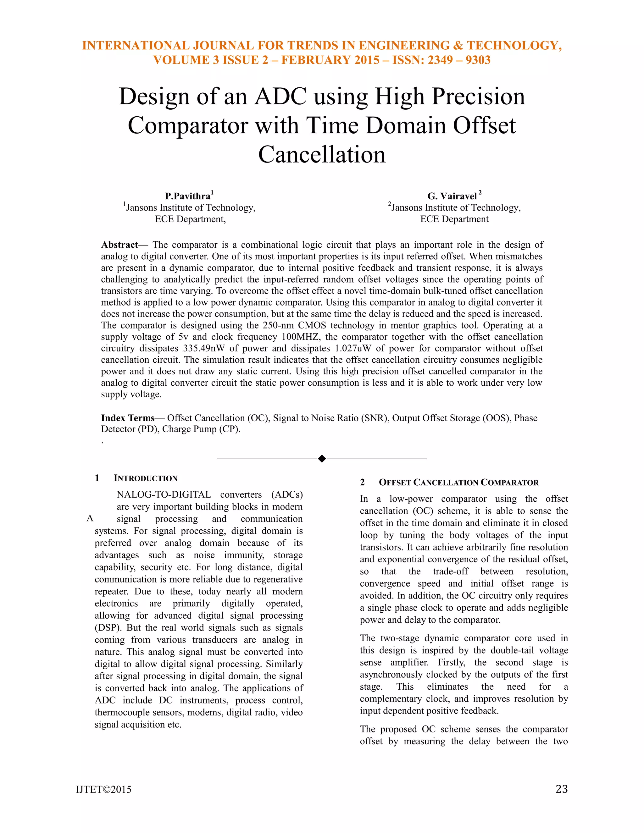
In a low-power comparator using the offset
cancellation (OC) scheme, it is able to sense the
offset in the time domain and eliminate it in closed
loop by tuning the body voltages of the input
transistors. It can achieve arbitrarily fine resolution
and exponential convergence of the residual offset,
so that the trade-off between resolution,
convergence speed and initial offset range is
avoided. In addition, the OC circuitry only requires
a single phase clock to operate and adds negligible
power and delay to the comparator.
The two-stage dynamic comparator core used in
this design is inspired by the double-tail voltage
sense amplifier. Firstly, the second stage is
asynchronously clocked by the outputs of the first
stage. This eliminates the need for a
complementary clock, and improves resolution by
input dependent positive feedback.
The proposed OC scheme senses the comparator
offset by measuring the delay between the two
A
INTERNATIONAL JOURNAL FOR TRENDS IN ENGINEERING & TECHNOLOGY,
VOLUME 3 ISSUE 2 – FEBRUARY 2015 – ISSN: 2349 – 9303
IJTET©2015 24
outputs and cancels it by tuning the body voltages
of the input transistors. In the ideal case in which
all the transistors are matched, if the two inputs of
the comparator are equal, Vo+ and Vo- will fall
simultaneously at an identical rate at the falling
edge of clock, whereas in the presence of offset,
they will not. Therefore, the input-referred offset
can be represented by the delay between the two
complementary outputs when there is no
differential input. A phase detector (PD) detects the
polarity and magnitude of this delay and drives a
charge pump (CP). The CP changes the body
voltages of the comparator input transistors stored
in the capacitors Cb+ and Cb-.
The body voltage affects the threshold as given in the
(1) as
(1)
where Vtp is the threshold of the input transistor,
Vt0 is the threshold with zero body bias, and γ, f are
process dependent parameters.
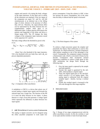
Fig. 1. Comparator offset cancellation
A multiplexer or MUX is a device that selects one of
several analog or digital input signals and forwards the
selected input into a single line. The function of the PD
is to sense the delay between its two inputs. A phase
detector is a logic circuit that generates a voltage signal
which represents the difference in phase between two
input signals.
3 ADC WITH OFFSET CANCELLATION COMPARATOR
The analog to digital converter can be designed using
the offset cancelled comparator to work under low
power consumption. Using this scheme in ADC it does
not increase the power consumption, but at the same
time the delay is reduced and the speed is increased.
Fig. 2. The block diagram of the system
To achieve a high conversion speed, the simplest and
potentially the fastest, flash architecture is used in this
architecture. In a flash architecture, clocked comparators
offer polarity sampling as one of the advantage to the
circuit. Consequently, the comparator outputs constitute
a thermometer code, which is converted to binary by the
decoder. Comparators often incorporate clocked
regenerative amplifiers to achieve a high speed. In this
ADC architecture the design flows through the
following steps.
1. First, the input signal is captured by the sample
and hold amplifier.
2. Second, this signal is quantized by the sub-
ADC, which produces a digital output.
3. Third, this digital signal goes to the sub-DAC
which converts it to an analog signal. This
analog signal is subtracted from the original
sampled signal - thereby, leaving a residual
signal.
4. Fourth, this residual signal is increased to the
full scale through the inter-stage amplifier.
4 IMPLEMENTATION
Fig. 3. Design of two stage comparatorcircuit with the
offset cancellation circuitry. In this the switches s1 and
s2 are open and the switches s3 and s4 are kept closed.
INTERNATIONAL JOURNAL FOR TRENDS IN ENGINEERING & TECHNOLOGY,
VOLUME 3 ISSUE 2 – FEBRUARY 2015 – ISSN: 2349 – 9303
IJTET©2015 25
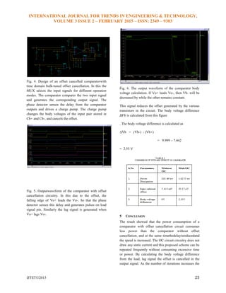
Fig. 4. Design of an offset cancelled comparatorwith
time domain bulk-tuned offset cancellation. In this the
MUX selects the input signals for different operation
modes. The comparator compares the two input signal
and generates the corresponding output signal. The
phase detector senses the delay from the comparator
outputs and drives a charge pump. The charge pump
changes the body voltages of the input pair stored in
Cb+ and Cb-, and cancels the offset.
Fig. 5. Outputwaveform of the comparator with offset
cancellation circuitry. In this due to the offset, the
falling edge of Vo+ leads the Vo-. So that the phase
detector senses this delay and generates pulses on lead
signal pin. Similarly the lag signal is generated when
Vo+ lags Vo-.
Fig. 6. The output waveform of the comparator body
voltage calculation. If Vo+ leads Vo-, then Vb- will be
decreased by while the other remains constant.
This signal reduces the offset generated by the various
transistors in the circuit. The body voltage difference
∆𝑉𝑏 is calculated from this figure
. The body voltage difference is calculated as
ΔVb = (Vb-) - (Vb+)
= 9.999 – 7.442
= 2.55 V
5 CONCLUSION
The result showed that the power consumption of a
comparator with offset cancellation circuit consumes
less power than the comparator without offset
cancellation, and at the same timethedelayisreducedand
the speed is increased. The OC circuit circuitry does not
draw any static current and this proposed scheme can be
repeated frequently without consuming excessive time
or power. By calculating the body voltage difference
from the lead, lag signal the offset is cancelled in the
output signal. As the number of iterations increases the
INTERNATIONAL JOURNAL FOR TRENDS IN ENGINEERING & TECHNOLOGY,
VOLUME 3 ISSUE 2 – FEBRUARY 2015 – ISSN: 2349 – 9303
IJTET©2015 26
offset can be proportionally reduced. It is worth noting
that both the proposed comparator and OC scheme are
very amenable to process scaling because of their
dynamic and time-domain operation. While the
accuracy of the circuit will be degraded due to the
reduced drain resistance, the proposed scheme will
actually benefit from smaller feature size because it can
provide smaller parasitic capacitance and higher time
resolution. The design is also tolerant to supply scaling
because there is no stacking of transistors.
REFERENCES
[1] Hamed S.M., Khalil A.H., Abdelhalim M.B., Amer
H.H. & Madian A.H., 2011, ―Testing of one stage
Pipelined Analog to Digital converter,‖
Proceedings of the International Conference on
Computer Engineering & Systems, Cairo, Egypt.
[2] He J., Zhan S., Chen D., and Geiger R.L., 2009,
―Analyses of static and dynamic random offset
voltages in dynamic comparators,” IEEETrans.
Circuits Syst. I, Reg. Papers, vol. 56, no. 5, pp.
911–919.
[3] Hong H.C. and Lee G.M., 2007, ―A 65-
fJ/conversion-step 0.9-V 200-kS/s rail-to-rail 8-bit
successive approximation ADC,‖ IEEE J. Solid-
StateCircuits, vol. 42, no. 10, pp. 2161–2168,.
[4] Jung Y., Lee S., Chae J., and Temes G.C., 2011,
―Low-power and low-offset comparator using latch
load,” IEEE Electron. Lett., vol. 47, no. 3, pp. 167–
168.
[5] Kentaro Yoshioka, Akira Shikata, Ryota Sekimoto
and Hiroki Ishikuro, 2014, ―An 8bit 0.3-0.8 V 0.2-
40 MS/s 2-bit/Step SAR ADC with successively
activated threshold configuring comparators in
40nm CMOS‖, IEEE Trans. On VLSI.
[6] Lee S.K. , Park S.J. , Park H.J. , and Sim J.Y. ,
2011, ―A 21 fJ/conversion step 100 KS /s 10-bit
ADC with a low-noise time-domain comparator for
low-power sensor interface,‖ IEEE J. Solid-State
Circuits, vol. 46, no. 3, pp. 651–659.
[7] Lu J. and Holleman J., 2012, ―A low-power
dynamic comparator with time domain bulk-driven
offset cancellation,‖ in Proc. IEEE Int. Symp.
Circuits Syst., pp. 2493–2496.
[8] Miyahara M. and Matsuzawa A.,2009, ―A low-
offset latched comparator using zero-static power
dynamic offset cancellation technique,‖ in Proc.
IEEE Asian Solid State Conf., pp. 233–236.
[9] Miyahara M., Asada Y., D. Paik, and Matsuzawa
A., 2008, ―A low-noise self-calibrating dynamic
comparator for high-speed ADCs,‖ in Proc. IEEE
Asian Solid State Conf., pp. 269–272.
[10] Nikoozadeh S. and Murmann B., 2006, ―An
analysis of latch comparator offset due to load
capacitor mismatch,” IEEE Trans. Circuits Syst.
II,Exp. Briefs, vol. 53, no. 12, pp. 1398–1402.
[11] Raja Mohd. Noor Hafizi Raja Daud and Labonnah
Farzana Rahman, 2012, ―Design and Analysis of
Low Power and High Speed Dynamic Latch
comparator in 0.18 um CMOS process‖, in
International Journal of Information Engineering,
Vol. 2, No. 6.
[12] Rajendran D.B., 2011, ―Design of Pipelined
Analog-to-Digital Converter with SI Technique in
65 nm CMOS Technology,‖ Master Thesis,
Department of Electrical Engineering, Linköping,
Sweden.
[13] Razavi B., 2000, ―Design of Analog CMOS
Integrated Circuits‖, McGraw Hill.
[14] Taehwan, Hariprasath Venkatram and Un-Ku
Moon, 2014, ―A time-based pipelined ADC using
both voltage and time domain information,‖ IEEE
J. Solid-State Circuits, vol. 49.

Design of an ADC using High Precision Comparator with Time Domain Offset Cancellation

  • 1.
    INTERNATIONAL JOURNAL FORTRENDS IN ENGINEERING & TECHNOLOGY, VOLUME 3 ISSUE 2 – FEBRUARY 2015 – ISSN: 2349 – 9303 IJTET©2015 23 Design of an ADC using High Precision Comparator with Time Domain Offset Cancellation P.Pavithra1 1 Jansons Institute of Technology, ECE Department, G. Vairavel 2 2 Jansons Institute of Technology, ECE Department Abstract— The comparator is a combinational logic circuit that plays an important role in the design of analog to digital converter. One of its most important properties is its input referred offset. When mismatches are present in a dynamic comparator, due to internal positive feedback and transient response, it is always challenging to analytically predict the input-referred random offset voltages since the operating points of transistors are time varying. To overcome the offset effect a novel time-domain bulk-tuned offset cancellation method is applied to a low power dynamic comparator. Using this comparator in analog to digital converter it does not increase the power consumption, but at the same time the delay is reduced and the speed is increased. The comparator is designed using the 250-nm CMOS technology in mentor graphics tool. Operating at a supply voltage of 5v and clock frequency 100MHZ, the comparator together with the offset cancellation circuitry dissipates 335.49nW of power and dissipates 1.027uW of power for comparator without offset cancellation circuit. The simulation result indicates that the offset cancellation circuitry consumes negligible power and it does not draw any static current. Using this high precision offset cancelled comparator in the analog to digital converter circuit the static power consumption is less and it is able to work under very low supply voltage. Index Terms— Offset Cancellation (OC), Signal to Noise Ratio (SNR), Output Offset Storage (OOS), Phase Detector (PD), Charge Pump (CP). . ———————————————————— 1 INTRODUCTION NALOG-TO-DIGITAL converters (ADCs) are very important building blocks in modern signal processing and communication systems. For signal processing, digital domain is preferred over analog domain because of its advantages such as noise immunity, storage capability, security etc. For long distance, digital communication is more reliable due to regenerative repeater. Due to these, today nearly all modern electronics are primarily digitally operated, allowing for advanced digital signal processing (DSP). But the real world signals such as signals coming from various transducers are analog in nature. This analog signal must be converted into digital to allow digital signal processing. Similarly after signal processing in digital domain, the signal is converted back into analog. The applications of ADC include DC instruments, process control, thermocouple sensors, modems, digital radio, video signal acquisition etc. 2 OFFSET CANCELLATION COMPARATOR In a low-power comparator using the offset cancellation (OC) scheme, it is able to sense the offset in the time domain and eliminate it in closed loop by tuning the body voltages of the input transistors. It can achieve arbitrarily fine resolution and exponential convergence of the residual offset, so that the trade-off between resolution, convergence speed and initial offset range is avoided. In addition, the OC circuitry only requires a single phase clock to operate and adds negligible power and delay to the comparator. The two-stage dynamic comparator core used in this design is inspired by the double-tail voltage sense amplifier. Firstly, the second stage is asynchronously clocked by the outputs of the first stage. This eliminates the need for a complementary clock, and improves resolution by input dependent positive feedback. The proposed OC scheme senses the comparator offset by measuring the delay between the two A
  • 2.
    INTERNATIONAL JOURNAL FORTRENDS IN ENGINEERING & TECHNOLOGY, VOLUME 3 ISSUE 2 – FEBRUARY 2015 – ISSN: 2349 – 9303 IJTET©2015 24 outputs and cancels it by tuning the body voltages of the input transistors. In the ideal case in which all the transistors are matched, if the two inputs of the comparator are equal, Vo+ and Vo- will fall simultaneously at an identical rate at the falling edge of clock, whereas in the presence of offset, they will not. Therefore, the input-referred offset can be represented by the delay between the two complementary outputs when there is no differential input. A phase detector (PD) detects the polarity and magnitude of this delay and drives a charge pump (CP). The CP changes the body voltages of the comparator input transistors stored in the capacitors Cb+ and Cb-. The body voltage affects the threshold as given in the (1) as (1) where Vtp is the threshold of the input transistor, Vt0 is the threshold with zero body bias, and γ, f are process dependent parameters. Fig. 1. Comparator offset cancellation A multiplexer or MUX is a device that selects one of several analog or digital input signals and forwards the selected input into a single line. The function of the PD is to sense the delay between its two inputs. A phase detector is a logic circuit that generates a voltage signal which represents the difference in phase between two input signals. 3 ADC WITH OFFSET CANCELLATION COMPARATOR The analog to digital converter can be designed using the offset cancelled comparator to work under low power consumption. Using this scheme in ADC it does not increase the power consumption, but at the same time the delay is reduced and the speed is increased. Fig. 2. The block diagram of the system To achieve a high conversion speed, the simplest and potentially the fastest, flash architecture is used in this architecture. In a flash architecture, clocked comparators offer polarity sampling as one of the advantage to the circuit. Consequently, the comparator outputs constitute a thermometer code, which is converted to binary by the decoder. Comparators often incorporate clocked regenerative amplifiers to achieve a high speed. In this ADC architecture the design flows through the following steps. 1. First, the input signal is captured by the sample and hold amplifier. 2. Second, this signal is quantized by the sub- ADC, which produces a digital output. 3. Third, this digital signal goes to the sub-DAC which converts it to an analog signal. This analog signal is subtracted from the original sampled signal - thereby, leaving a residual signal. 4. Fourth, this residual signal is increased to the full scale through the inter-stage amplifier. 4 IMPLEMENTATION Fig. 3. Design of two stage comparatorcircuit with the offset cancellation circuitry. In this the switches s1 and s2 are open and the switches s3 and s4 are kept closed.
  • 3.
    INTERNATIONAL JOURNAL FORTRENDS IN ENGINEERING & TECHNOLOGY, VOLUME 3 ISSUE 2 – FEBRUARY 2015 – ISSN: 2349 – 9303 IJTET©2015 25 Fig. 4. Design of an offset cancelled comparatorwith time domain bulk-tuned offset cancellation. In this the MUX selects the input signals for different operation modes. The comparator compares the two input signal and generates the corresponding output signal. The phase detector senses the delay from the comparator outputs and drives a charge pump. The charge pump changes the body voltages of the input pair stored in Cb+ and Cb-, and cancels the offset. Fig. 5. Outputwaveform of the comparator with offset cancellation circuitry. In this due to the offset, the falling edge of Vo+ leads the Vo-. So that the phase detector senses this delay and generates pulses on lead signal pin. Similarly the lag signal is generated when Vo+ lags Vo-. Fig. 6. The output waveform of the comparator body voltage calculation. If Vo+ leads Vo-, then Vb- will be decreased by while the other remains constant. This signal reduces the offset generated by the various transistors in the circuit. The body voltage difference ∆𝑉𝑏 is calculated from this figure . The body voltage difference is calculated as ΔVb = (Vb-) - (Vb+) = 9.999 – 7.442 = 2.55 V 5 CONCLUSION The result showed that the power consumption of a comparator with offset cancellation circuit consumes less power than the comparator without offset cancellation, and at the same timethedelayisreducedand the speed is increased. The OC circuit circuitry does not draw any static current and this proposed scheme can be repeated frequently without consuming excessive time or power. By calculating the body voltage difference from the lead, lag signal the offset is cancelled in the output signal. As the number of iterations increases the
  • 4.
    INTERNATIONAL JOURNAL FORTRENDS IN ENGINEERING & TECHNOLOGY, VOLUME 3 ISSUE 2 – FEBRUARY 2015 – ISSN: 2349 – 9303 IJTET©2015 26 offset can be proportionally reduced. It is worth noting that both the proposed comparator and OC scheme are very amenable to process scaling because of their dynamic and time-domain operation. While the accuracy of the circuit will be degraded due to the reduced drain resistance, the proposed scheme will actually benefit from smaller feature size because it can provide smaller parasitic capacitance and higher time resolution. The design is also tolerant to supply scaling because there is no stacking of transistors. REFERENCES [1] Hamed S.M., Khalil A.H., Abdelhalim M.B., Amer H.H. & Madian A.H., 2011, ―Testing of one stage Pipelined Analog to Digital converter,‖ Proceedings of the International Conference on Computer Engineering & Systems, Cairo, Egypt. [2] He J., Zhan S., Chen D., and Geiger R.L., 2009, ―Analyses of static and dynamic random offset voltages in dynamic comparators,” IEEETrans. Circuits Syst. I, Reg. Papers, vol. 56, no. 5, pp. 911–919. [3] Hong H.C. and Lee G.M., 2007, ―A 65- fJ/conversion-step 0.9-V 200-kS/s rail-to-rail 8-bit successive approximation ADC,‖ IEEE J. Solid- StateCircuits, vol. 42, no. 10, pp. 2161–2168,. [4] Jung Y., Lee S., Chae J., and Temes G.C., 2011, ―Low-power and low-offset comparator using latch load,” IEEE Electron. Lett., vol. 47, no. 3, pp. 167– 168. [5] Kentaro Yoshioka, Akira Shikata, Ryota Sekimoto and Hiroki Ishikuro, 2014, ―An 8bit 0.3-0.8 V 0.2- 40 MS/s 2-bit/Step SAR ADC with successively activated threshold configuring comparators in 40nm CMOS‖, IEEE Trans. On VLSI. [6] Lee S.K. , Park S.J. , Park H.J. , and Sim J.Y. , 2011, ―A 21 fJ/conversion step 100 KS /s 10-bit ADC with a low-noise time-domain comparator for low-power sensor interface,‖ IEEE J. Solid-State Circuits, vol. 46, no. 3, pp. 651–659. [7] Lu J. and Holleman J., 2012, ―A low-power dynamic comparator with time domain bulk-driven offset cancellation,‖ in Proc. IEEE Int. Symp. Circuits Syst., pp. 2493–2496. [8] Miyahara M. and Matsuzawa A.,2009, ―A low- offset latched comparator using zero-static power dynamic offset cancellation technique,‖ in Proc. IEEE Asian Solid State Conf., pp. 233–236. [9] Miyahara M., Asada Y., D. Paik, and Matsuzawa A., 2008, ―A low-noise self-calibrating dynamic comparator for high-speed ADCs,‖ in Proc. IEEE Asian Solid State Conf., pp. 269–272. [10] Nikoozadeh S. and Murmann B., 2006, ―An analysis of latch comparator offset due to load capacitor mismatch,” IEEE Trans. Circuits Syst. II,Exp. Briefs, vol. 53, no. 12, pp. 1398–1402. [11] Raja Mohd. Noor Hafizi Raja Daud and Labonnah Farzana Rahman, 2012, ―Design and Analysis of Low Power and High Speed Dynamic Latch comparator in 0.18 um CMOS process‖, in International Journal of Information Engineering, Vol. 2, No. 6. [12] Rajendran D.B., 2011, ―Design of Pipelined Analog-to-Digital Converter with SI Technique in 65 nm CMOS Technology,‖ Master Thesis, Department of Electrical Engineering, Linköping, Sweden. [13] Razavi B., 2000, ―Design of Analog CMOS Integrated Circuits‖, McGraw Hill. [14] Taehwan, Hariprasath Venkatram and Un-Ku Moon, 2014, ―A time-based pipelined ADC using both voltage and time domain information,‖ IEEE J. Solid-State Circuits, vol. 49.