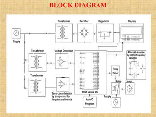
This document describes a project to detect failures in synchronizing a generator's power output with an electric grid. It discusses:
- The importance of synchronizing a generator's voltage, frequency, and phase with the grid before connecting.
- How synchronization can be done manually or automatically to prevent abnormalities in voltage and frequency.
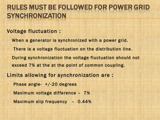
- Limits for phase angle, voltage difference, and slip frequency during synchronization.
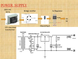
- A hardware system using a microcontroller, timers, comparators, and other components to detect synchronization failures like under/over voltage or frequency.
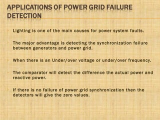
- Applications include solar power plants and providing uninterrupted power where grid synchronization is important.