Download to read offline
![International Journal of VLSI design & Communication Systems (VLSICS) Vol.7, No.4, August 2016
27
Table 3 Result comparison table
5. CONCLUSION AND FUTURE SCOPE
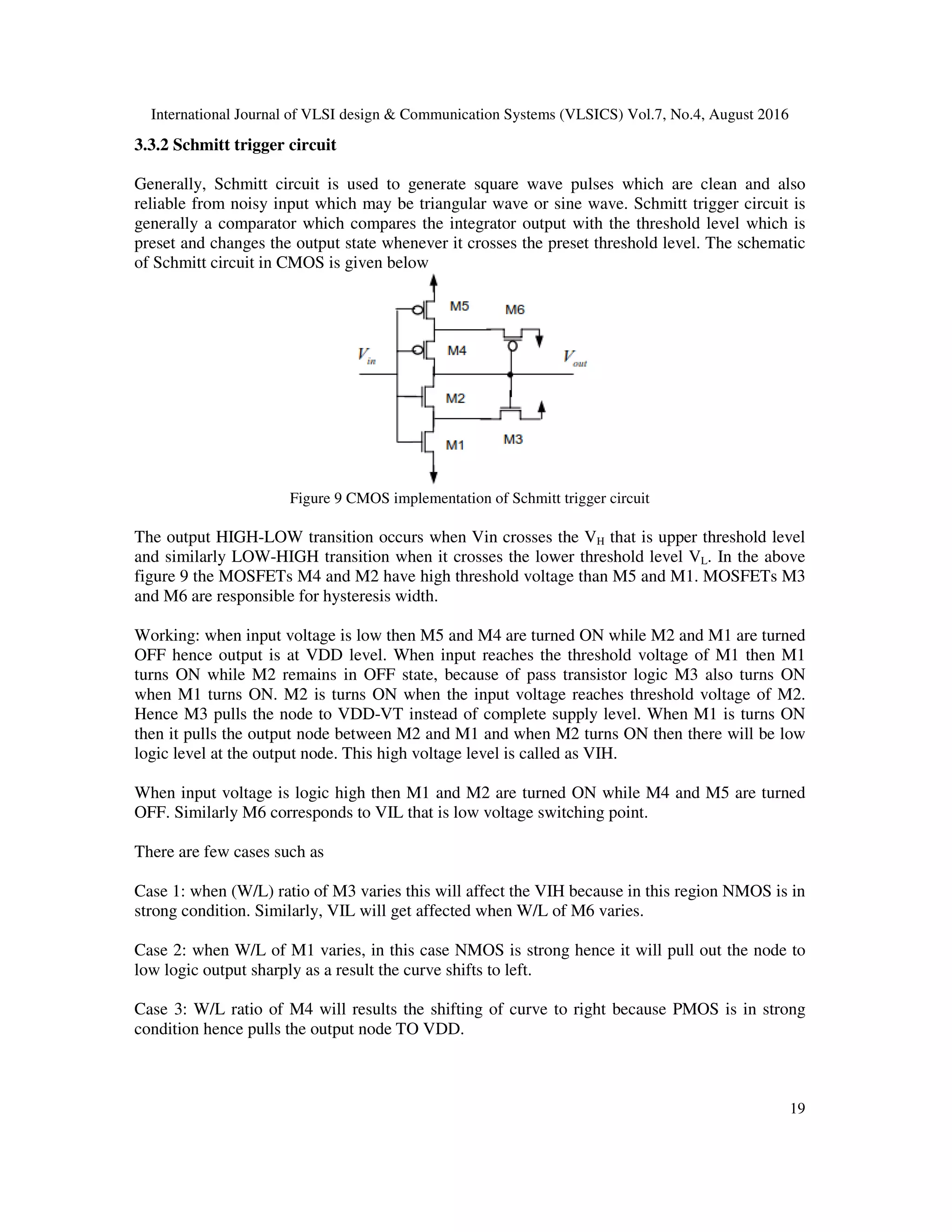
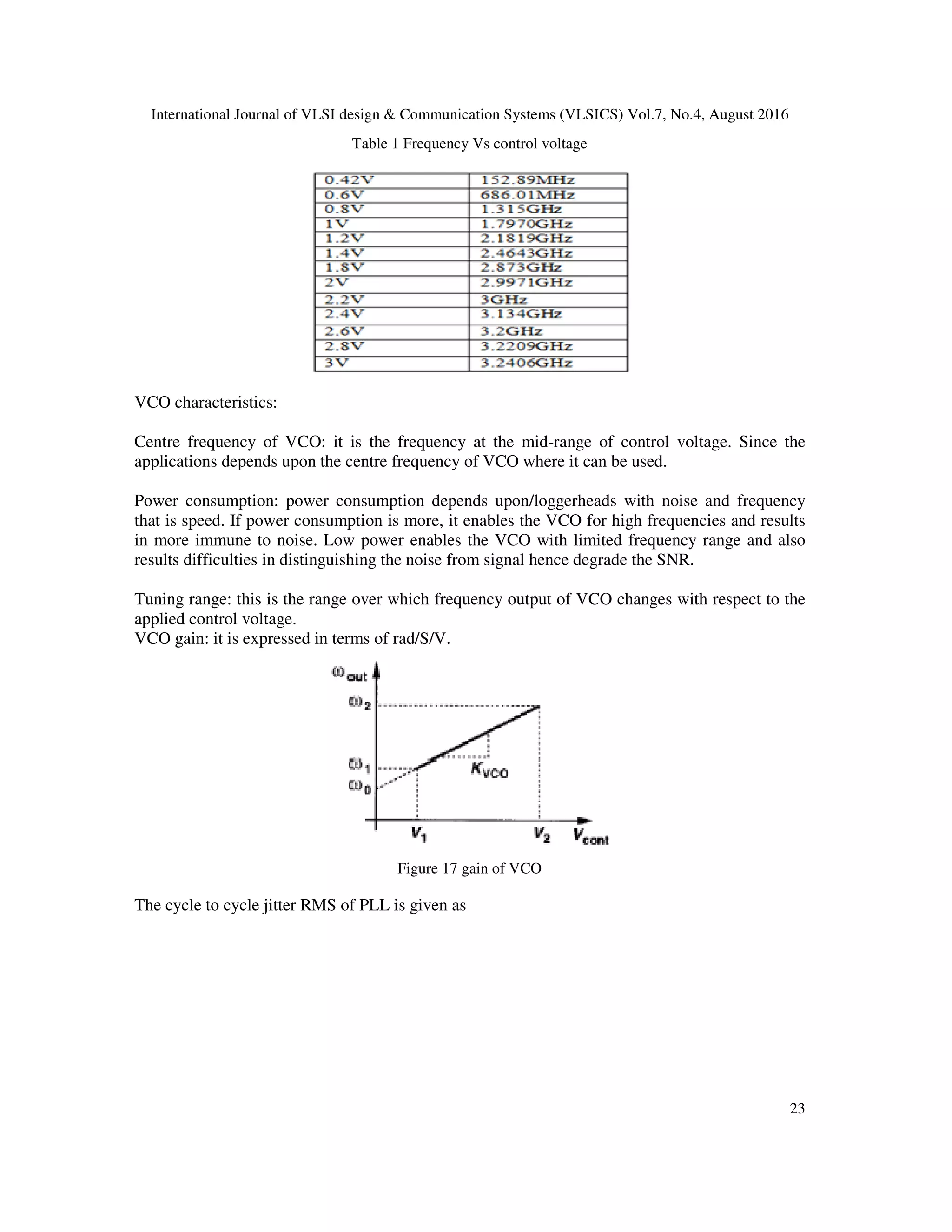
The PLL in this paper is designed in 130nm technology using Mentor Graphics tool. The
designed PLL is locked by generating 1.312GHz frequency output signal which can be used for
RF wireless communication system. The PLL has jitter RMS value of 5.98ps and peak-peak jitter
RMS is 4.2652ns, these two parameters are important factor for ADC and RF systems. If jitter is
more than it will produces timing issues which are required for clock synchronization and
distribution in systems such as medical imaging, ADC, DAC and Communication System The
power consumption of PLL is 58mW. The power consumption of VCO designed is 24.4113µW
for 1V supply which has limited frequency range hence used for low power applications which is
required for longer battery life. The power consumption of VCO for 3V supply is 11.04mW
which has frequency range from 0.152GHz to 3.240GHz, hence used in HF applications. The
phase margin for implemented PLL is 66.280
. The phase noise of VCO at 10MHz frequency is -
130dBc/Hz. The future scope of design is further reduction of jitter RMS value by applying
power grid circuit which consists of R and C to the entire circuit [16].
REFERENCES
[1] J. Craninckx and M. Steyaert, “A 1.8-GHz low-phase noise CMOS VCO using optimized hollow
spiral inductors,” IEEE J. Solid-State Circuits, vol. 32, pp. 736–744, May 1997.
[2] Yalcin, A.E. and P. John, 2004. A 5.9-GHz voltage controlled ring Oscillator in 0.18 um CMOS
technology. IEEE J. Solid-State Circuit, 39(1): 230-233.
[3] C. H. Park and B. Kim, “A low-noise, 900-MHz VCO in 0.6-m CMOS” IEEE J. Solid-State Circuits,
vol. 34, pp. 586–591, May 1999.
[4] A. Hajimiri, S. Limotyrakis, and T. H. Lee, “Phase noise in multi-gigahertz CMOS ring oscillators,”
in Proc. IEEE 1998 Custom Integrated Circuit Conf., 1998, pp. 49–52.
[5] T. Friedrich, “Direct phase noise measurements using a modern spectrum analyser,” microwave J,
vol. 35,pp. 94,96,99,101-104, Aug. 1992.](https://image.slidesharecdn.com/7416vlsi02-160907052306/75/DESIGN-OF-DIGITAL-PLL-USING-OPTIMIZED-PHASE-NOISE-VCO-15-2048.jpg)
![International Journal of VLSI design & Communication Systems (VLSICS) Vol.7, No.4, August 2016
28
[6] K. M. Ring and S. Krishnan, “Long-term jitter reduction through supply noise compensation,” in
Proceedings of the IEEE International Symposium on Circuits and Systems (ISCAS’08), pp. 2382–
2385, Seattle, Wash, USA, May 2008.
[7] Y. Chen, Z. Wang and L. Zhang, “A 5GHz 0.18-µm CMOS technology PLL with a symmetry
PFD,” in Proceedings of the International Conference on Microwave and Millimetre Wave
Technology (ICMMT’08), vol. 2, pp. 562–565, Nanjing, China, April 2008
[8] Rahajandraibe, A.W., L. Zaid, V.C. de Beaupre and J. Roche, 2007. Low-gain-wide-range 2.4-GHz
phase locked loop. 14th IEEE International Conference on Electronics, Circuits and Systems, pp: 26-
29.
[9] S. B. Rashmi and Siva S. Yellampalli, “Design of Phase Frequency Detector and Charge Pump for
High Frequency PLL,” International Journal of Soft Computing and Engineering, vol.2, Issue-2, May
2012, pp 88-92.
[10] V.Lule and V.Nasre, “Area efficient 0.18um CMOS phase frequency detector for high speed PLL”,
International Journal of Engineering Scientific and Research Publication, vol.2, Feb. 2012, pp 1-3.
[11] Chakraborty, B. and R.R. Pal, 2007. Study of speed enhancement of a CMOS ring VCO. J. Phys.
Sci., 11: 77-86.
[12] M. Shahruz, “Novel phase-locked loops with enhanced locking capabilities,” Journal of Sound and
Vibration, Vol. 241, Issue 3, Pages 513-523, 29 March 2001.
[13] Sung-Rung Han, Chi-Nan Chuang, and Shen-Iuan Liu, Member, IEEE, "A Time-Constant Calibrated
Phase-Locked Loop With a Fast-Locked Time", IEEE transactions on circuits and systems, vol. 54,
no. 1, January.
[14] Behzad Razavi, “Design of Analog CMOS Integrated Circuits”.
[15] Ronald E. Best, “Phase-Locked Loop Design, Simulation and Applications” Fifth Edition.
[16] Bo Zhao and Huazhong Yang “ Supply-Noise Interactions Among Sub modules Inside a Charge-
Pump PLL” IEEE Transactions on Very Large Scale Integration (VLSI) Systems, year: 2015,
Volume: 23, Issue: 4.](https://image.slidesharecdn.com/7416vlsi02-160907052306/75/DESIGN-OF-DIGITAL-PLL-USING-OPTIMIZED-PHASE-NOISE-VCO-16-2048.jpg)

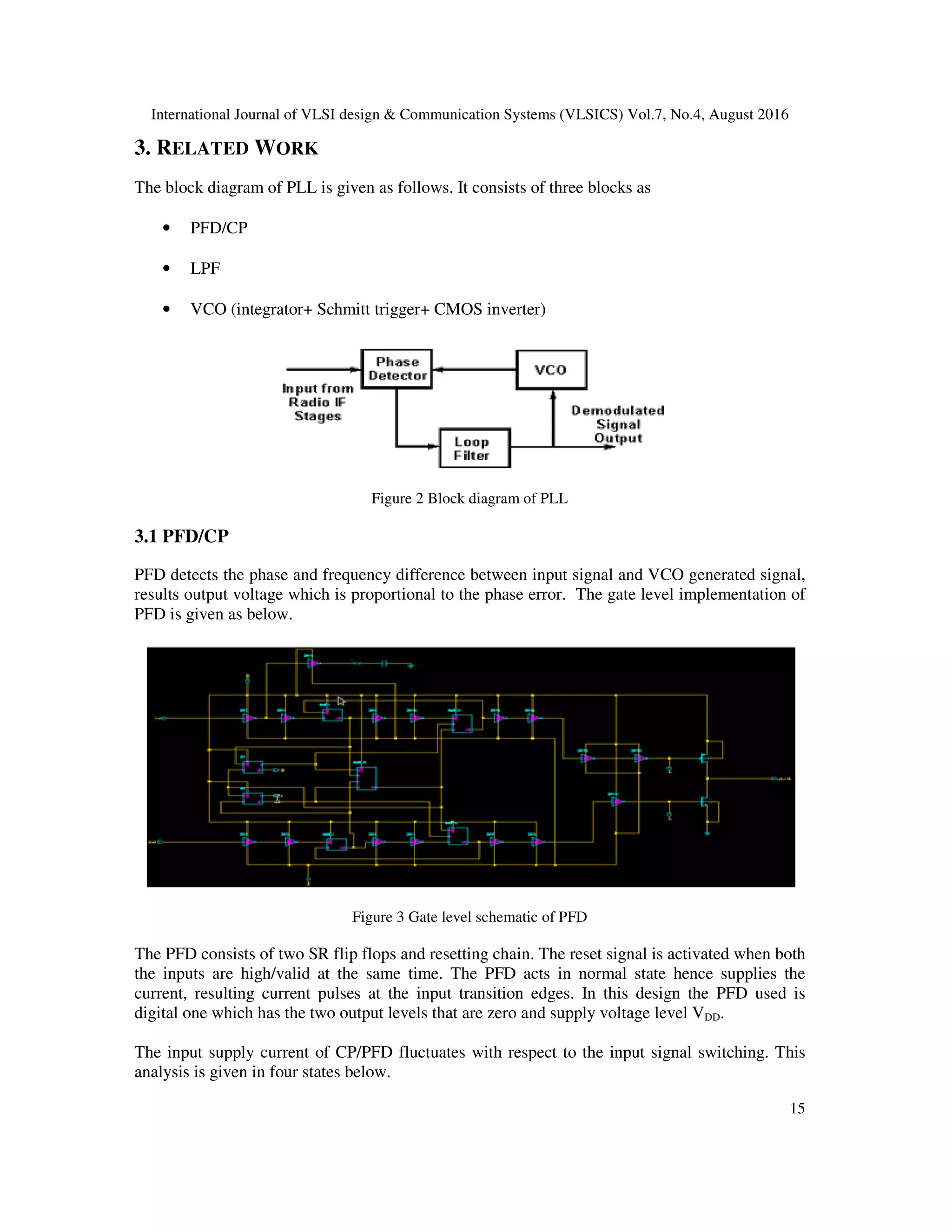
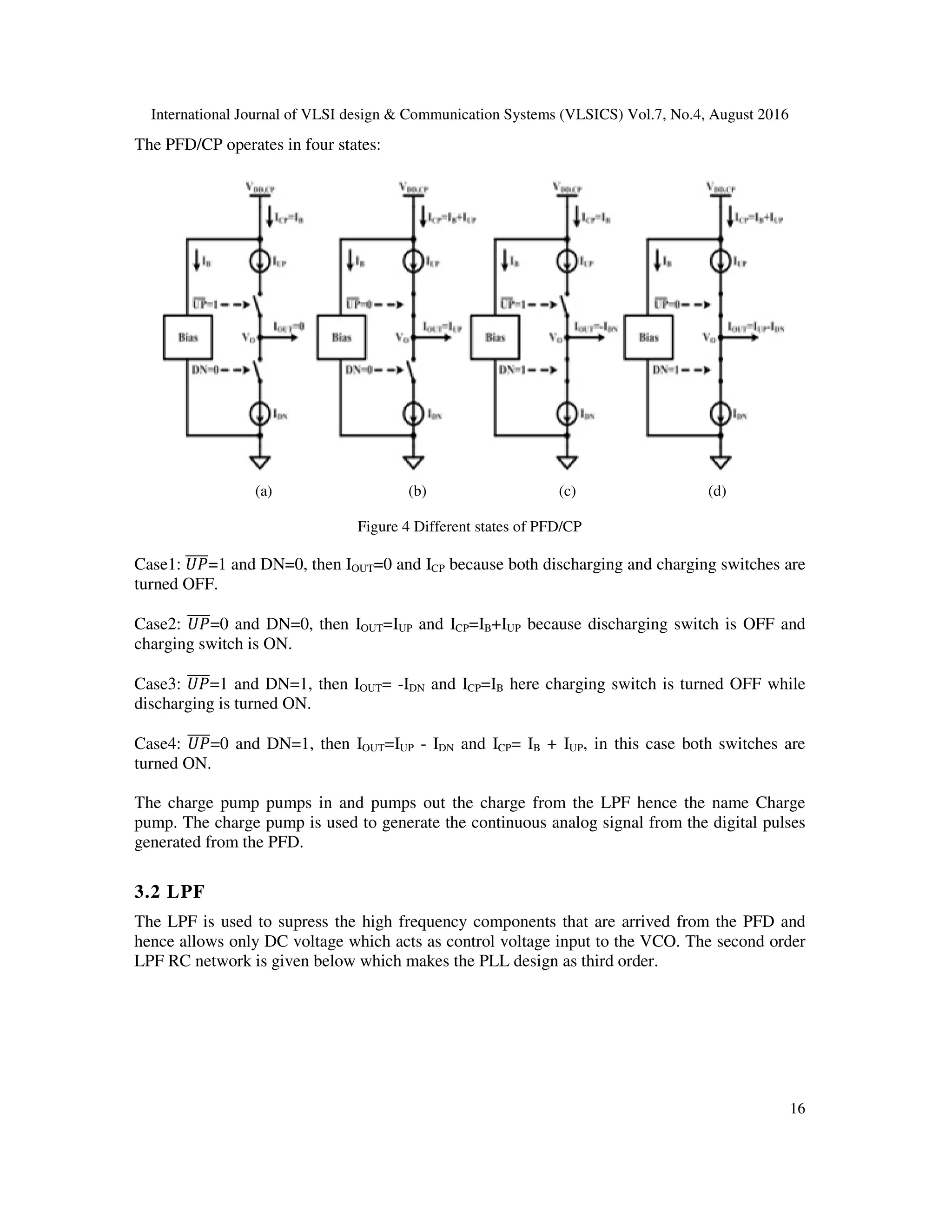
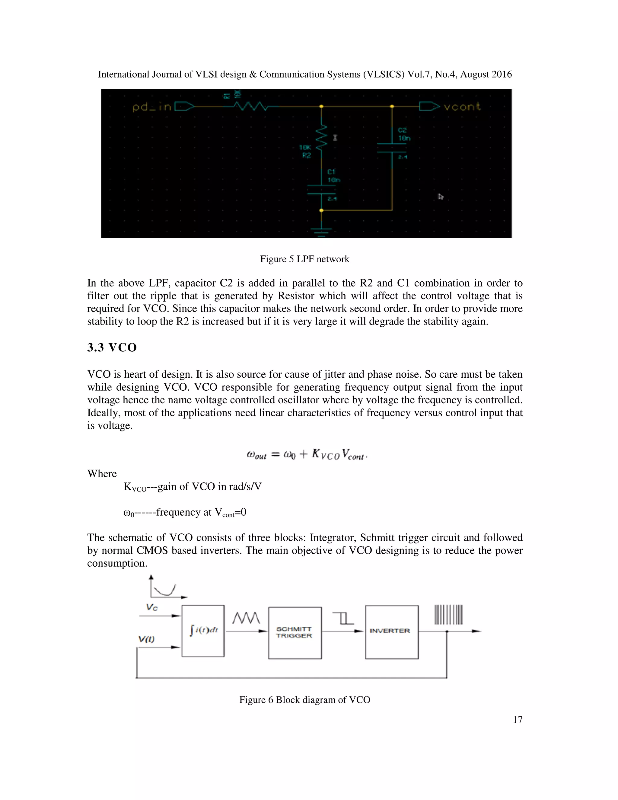
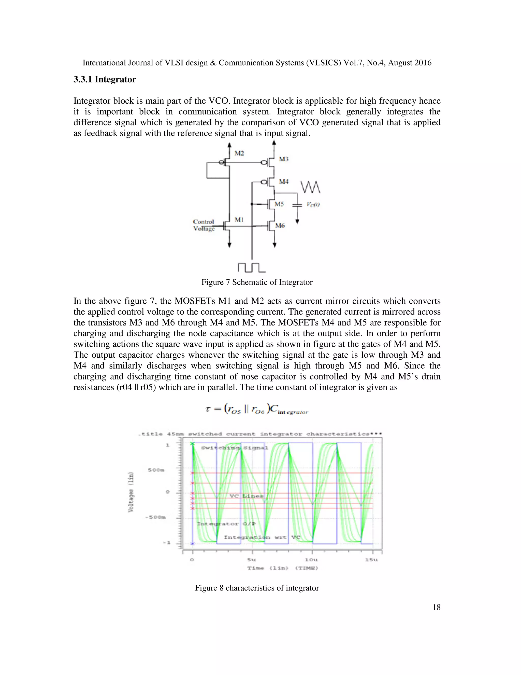
This paper presents the design of a digital phase-locked loop (PLL) using a current-starved or integrator voltage-controlled oscillator (VCO) in 130nm CMOS technology, focusing on minimizing phase noise and jitter for high-frequency applications. The PLL achieves an output frequency of 1.318 GHz with a phase noise of -130 dBc/Hz at a 10 MHz offset and a cycle-to-cycle jitter of 5.98 ps, making it suitable for wireless communication systems. Key advancements include the use of a Schmitt trigger circuit to enhance noise immunity and the implementation of a digital phase frequency detector to improve stability.