Downloaded 17 times
![IJRET: International Journal of Research in Engineering and Technology eISSN: 2319-1163 | pISSN: 2321-7308
_______________________________________________________________________________________
Volume: 05 Issue: 01 | Jan-2016, Available @ http://www.ijret.org 283
DESIGN AND ANALYSING OF COMPACT MICROSTRIP ANTENNA
WITH DEFECTED GROUND STRUCTURE FOR UWB APPLICATION
Rahul Sharma1
, A.N. Mishra2
1
ECE Department, Krishna Engineering College, Ghaziabad, India
2
ECE Department, Krishna Engineering College, Ghaziabad, India
Abstract
In this paper a small size microstrip antenna with DGS (Defected ground structure) is designed and analyzed for UWB(Ultra
Wide Band) application. This antenna cover the complete frequency range of 3.1 to 10.6 GHz with a very small geometry as
compared to a conventional antenna Dielectric substrate use in this antenna is Fr-4. This antenna is designed with a dimension is
36mm × 34 mm on a dielectric substrate Fr-4 whose permittivity εr =4.4 and height h = 1.6 mm. The result for return losses and
radiation patterns is simulated by using HFSS (High Frequency structure simulation) software. The High frequency structure
simulator is employed to analyze the planned antenna and simulated results on return loss, The ground element of the proposed
antenna is taken in the form of defected ground structure (DGS).
Keywords: Microstrip Antenna, UWB, DGS, Wide band, HFSS
--------------------------------------------------------------------***----------------------------------------------------------------------
1. INTRODUCTION
Micro strip patch antenna is wide beam width, narrowband
antenna. And consists of three major part there is ground,
patch, substrate (here used FR-4). There are numerous
substrates that can be used for the design of microstrip
antennas, and their dielectric constants are usually in the
range of 2.2 ≤ εr ≤ 12 [4][5] [6]. In this paper used Defected
Ground Structure technology. Defected Ground Structure is
unique technology to reduce the antenna size. A DGS may
come in a variety of geometries and sizes, depending upon
their mode of application, as well as the frequency of
operation [8][9]. The Defected Ground Structure (DGS)
technology are various type there is Dumbbell-shaped,
Square heads connected with U slots, H-shaped[9], Meander
line, U-shaped[9], T-shaped, DGS in T-shaped and
rectangular shaped. And Ultra wide band range (UWB)
released by Federal Communications Commission (FCC)
since 2002. It Covers frequency range 3.1 GHz to 10.3
GHz.[2] [3]. The ultra-wideband (UWB) systems
advantages is it is consist high speed data, small size, not
expensive, low complexity[1-4,1][10]. This antaean is
simulated by HFSS. HFSS is integral equation and method
of the moment based Electromagnetic simulator.
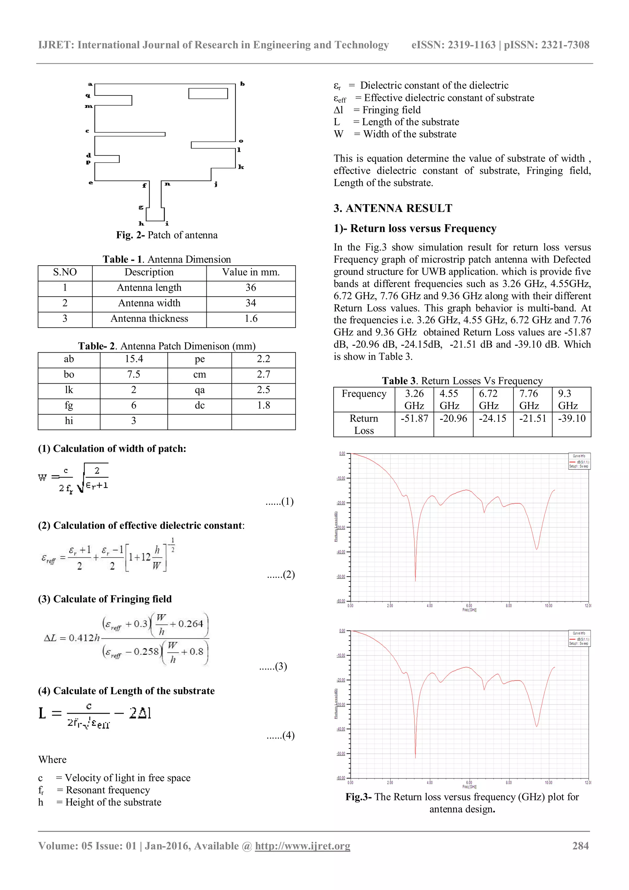
2. ANTENNA STRUCTURE AND EQUATION
In Fig. 1 and Fig. 2 show geometry of the proposed
microstrip patch antenna with DGS on the Fr4 substrate
together with its geometrical dimensions. In the table 1 and
table 2 also refer the dimension value of microstrip patch
antenna. Value of antenna is taken in mm. Also equation
1,2,3,4 are calculate the dimension of the microstrip
antenna.
.
A. Antenna Geometry
(a)
(b)
Fig.1- Microstrip antenna on FR-4 Substrate](https://image.slidesharecdn.com/designandanalysingofcompactmicrostripantennawithdefectedgroundstructureforuwbapplication-160919114351/75/Design-and-analysing-of-compact-microstrip-antenna-with-defected-ground-structure-for-uwb-application-1-2048.jpg)
![IJRET: International Journal of Research in Engineering and Technology eISSN: 2319-1163 | pISSN: 2321-7308
_______________________________________________________________________________________
Volume: 05 Issue: 01 | Jan-2016, Available @ http://www.ijret.org 285
2)- VSWR versus Frequency
In the Fig.4 show result for VSWR versus Frequency graph
of microstrip patch antenna with Defected ground structure
for UWB application. which is provide three different
VSWR value at the frequencies i.e. 4.55 GHz, 6.72 GHz and
7.76 GHz obtained VSWR values are 1.55 , 1.07, and 1.46.
Which is show in Table 4.
Table 4. VSWR Vs Frequency
Frequency 4.55 GHz 6.72 GHz 7.76 GHz
VSWR 1.55 1.07 1.46
Fig. 4 - VSWR versus frequency (GHz) plot for antenna
design.
3)- 3D Radiation Pattern of antenna
Fig. 5 - 3D Radiation Pattern of Antenna
IV. CONCLUSION
In this work, a Microstrip antenna with DGS for ultra wide
band (UWB) Application has been design and simulated.
This is a new patch antenna with defected Ground Structure
(DGS) properties: improved Return loss (S11 db), VSWR.
And the size of this antenna is small. Fundamental
parameters are modeled with the equations and estimated
with HFSS software. Microstrip patch antenna application in
as like Mobile Communication, Global Positioning System,
Interoperability for microwave access (Wi-Max), WLAN,
Cognitive Radio, and UWB
V. REFERENCES
[1] Chen, Z. N., X. H.Wu, H. F. Li, N. Yang, and M. Y. W.
Chia, Considerations for source pulses and antennas in
UWB radio systems," IEEE Trans. Antennas Propag.,
Vol. 52, 17391748,Jul. 2004
[2] Ultra-Wideband Operation FCC Report and Order,
Tech.Rep.US 47 CFR Part 15, 2002.
[3] UWB Antenna for wireless Application Osama Harz
and Abdul –reazik sebak chapter 6.
[4] NEWS Federal Communications Commission
http://transition.fcc.gov/Bureaus/Engineering_Technolo
gy/News_Releases/2002/nret0203.html
[5] H. Oraizi and S. Hedayati, “Miniaturized UWB
monopole Microstrip antenna design by the
combination of Giusepe Peano and Sierpinski carpet
fractals,” IEEE Antenna Wireless Propag. Lett., vol. 10,
pp. 67–70, 2011
[6] A. Balanis, “Antenna Theory and Analysis,” Third
Edition, John Wiley & Sons.
[7] Ramesh Garg, Prakash Bartia, Inder Bahl, Apisak
Ittipiboon, ‘’Microstrip Antenna Design Handbook’’,
2001
[8] Debatosh Guha, Sujoy Biswas and Chandrakanta
Kumar “Printed Antenna Designs Using Defected
Ground Structures: A Review of Fundamentals and
State-of-the-Art Developments Forum for
Electromagnetic Research Methods and Application
Technologies (FERMAT)
[9] J. Woo, T. K. Lee, J. W. Lee, C. S. Pyo, and W. K. Choi,
“Novel USlot and V-Slot DGSs for band stop filter with
improved Q factor,” IEEE Trans. Microwave Theory
and Techniques, vol. 54, no. 6, pp. 2840- 2847, June
2006
[10]Sanjeev Budhauliya, Bimal Raj Dutta, Arvind Kumar
“Iterated Pythagorean Fractal Tree Multiband
Antenna” International Journal of Scientific and
Research Publications, Volume 3, Issue 9, September
2013](https://image.slidesharecdn.com/designandanalysingofcompactmicrostripantennawithdefectedgroundstructureforuwbapplication-160919114351/75/Design-and-analysing-of-compact-microstrip-antenna-with-defected-ground-structure-for-uwb-application-3-2048.jpg)

The document presents the design and analysis of a compact microstrip antenna with a defected ground structure (DGS) for ultra-wideband (UWB) applications, specifically covering frequencies from 3.1 to 10.6 GHz. It details the antenna's dimensions, simulation results using HFSS software, including return loss and VSWR values, and establishes its advantages in various communication technologies. The study concludes that this new antenna design is efficient, compact, and effective for modern UWB applications.


