Downloaded 26 times
![IJRET: International Journal of Research in Engineering and Technology eISSN: 2319-1163 | pISSN: 2321-7308
_______________________________________________________________________________________
Volume: 04 Issue: 10 | Oct-2015, Available @ http://www.ijret.org 43
MICROSTRIP LOW PASS FILTER DESIGNS USING DEFECTED
GROUND STRUCTURE
Dhara Gadhvi1
, Urvik Shah2
1
Assistant Professor, Department of Electronics & Communication Engineering, Babaria Institue of Technology,
Gujarat, India
2
Assistant Professor, Department of Electronics & Communication Engineering, Babaria Institue of Technology,
Gujarat, India
Abstract
The microwave filters play an important role in most RF/microwave applications. They are designed to remove undesired
harmonics to reduce the system noise or to remove spurious mixing products. DGS slot with an interdigital shape are introduced
here in two elliptic low pass filter designs. Here a fifth order low pass filter was designed, simulated and fabricated for a cut off
frequency of 3GHz. Finally a prototype model were designed based on the simulation results obtained. These prototype filter
designs have more than 20 dB of stop band rejection and a good return loss in the pass band. The fabricated results proved to be
better than the simulation results. In the first low pas filter design the central aperture was replaced with the interdigital slot
structure which improved the stop band response at the resonant frequency around 7.8 GHz. To improve the stop band rejection
two interdigital structures were introduced in the bottom layer (Ground).
Key Words: Defected ground structure (DGS), low pass filters, microstrip filter, transmission zero.
--------------------------------------------------------------------***----------------------------------------------------------------------
1. INTRODUCTION
In recent years there is increasing demand for broader
bandwidth in wireless communication systems and many
researches are going on the wideband filters [1-4]. In this
work the Defected Ground Structures (DGS) [5-10]
presented here is to improve the performance of a traditional
microstrip low pass filters. The different applications in
passive circuits like low pass filters and band pass filters has
given origin to the Defected Ground Structure (DGS). The
Defected Ground structure (DGS) have better stop band
rejection which are helpful in improving characteristics of
certain devices like efficiency of power amplifiers is
increased, performance of certain amplifiers and antennas is
enhanced, harmonic filtering, also size of microwave
circuits is reduced. The resonant frequency of the microstrip
line structure is varied or controlled by modifying the shape
and size of the slot. For improving the pass band responses
of the microstrip filters useful design equations are given.
Here two elliptic low pass filter designs were designed and
simulated than fabricated on an FR-4 substrate with a
relative dielectric constant of 4.4 and thickness of 1.2mm
[3],[4]. One transmission zero is introduced in the first low
pass filter design by replacing the central aperture with
interdigital structure which consists of metal fingers. The
resonant frequency of the structure can be controlled by
varying the distance between these metal fingers but
keeping the area occupied by the slot constant. Two
transmission zeroes are introduced in the second low pass
filter design in the two slots with same finger lengths to
improve the stop band response. The two transmission zero
design has better response than one transmission zero design
for passband and stop band. The resonant frequency of the
slot can be varied without changing the slot size by
changing the number of metal fingers [13-20]. In the figure
1 the interdigital DGS slot [4] introduced here is shown. In
this technical note all dimensions are in mm. Under the
microstrip line in the top layer the slot is etched in the
bottom layer which is the ground metal layer. The major
advantage to this microstrip line is the tighter capacitive
coupling provided by the slot in the bottom layer with the
interdigital DGS. This replaces the slot capacitances by the
interdigital capacitance. The area of DGS can be reduced
effectively by using interdigital DGS in the design of
miniature devices. By modifying the number of metal
fingers keeping the slot size unchanged the change in
resonant frequency can be realized. In the one transmission
zero design the center slot is replaced by the interdigital
DGS where the slot has width of 4.9 mm and length of 5.65
mm. There are total 6 metal fingers which have a width of
0.4mm and length 3.2mm. By increasing length l of the
metal fingers the resonant frequency of the slot and
capacitance are increased. From the total 3 slots in the
bottom layer the dimensions of the center slot is as
described above and the other two slots have width 4.9 mm
and length of 3.75 mm. In the two transmission zero design
also the dimension of center slot is same as first design but
the other two slots are replaced by interdigital DGS where
the metal fingers are of width 0.535mm and length of 4mm.
By these changes in the low pass filter designs the resonance
is brought down to a remarkable level which is shown in fig.
11 and 12.
All the three fabricated low pass filter designs have the
length of 25.6 mm and breadth of 11.6mm.](https://image.slidesharecdn.com/microstriplowpassfilterdesignsusingdefectedgroundstructure-160919071249/85/Microstrip-low-pass-filter-designs-using-defected-ground-structure-1-320.jpg)
![IJRET: International Journal of Research in Engineering and Technology eISSN: 2319-1163 | pISSN: 2321-7308
_______________________________________________________________________________________
Volume: 04 Issue: 10 | Oct-2015, Available @ http://www.ijret.org 43
MICROSTRIP LOW PASS FILTER DESIGNS USING DEFECTED
GROUND STRUCTURE
Dhara Gadhvi1
, Urvik Shah2
1
Assistant Professor, Department of Electronics & Communication Engineering, Babaria Institue of Technology,
Gujarat, India
2
Assistant Professor, Department of Electronics & Communication Engineering, Babaria Institue of Technology,
Gujarat, India
Abstract
The microwave filters play an important role in most RF/microwave applications. They are designed to remove undesired
harmonics to reduce the system noise or to remove spurious mixing products. DGS slot with an interdigital shape are introduced
here in two elliptic low pass filter designs. Here a fifth order low pass filter was designed, simulated and fabricated for a cut off
frequency of 3GHz. Finally a prototype model were designed based on the simulation results obtained. These prototype filter
designs have more than 20 dB of stop band rejection and a good return loss in the pass band. The fabricated results proved to be
better than the simulation results. In the first low pas filter design the central aperture was replaced with the interdigital slot
structure which improved the stop band response at the resonant frequency around 7.8 GHz. To improve the stop band rejection
two interdigital structures were introduced in the bottom layer (Ground).
Key Words: Defected ground structure (DGS), low pass filters, microstrip filter, transmission zero.
--------------------------------------------------------------------***----------------------------------------------------------------------
1. INTRODUCTION
In recent years there is increasing demand for broader
bandwidth in wireless communication systems and many
researches are going on the wideband filters [1-4]. In this
work the Defected Ground Structures (DGS) [5-10]
presented here is to improve the performance of a traditional
microstrip low pass filters. The different applications in
passive circuits like low pass filters and band pass filters has
given origin to the Defected Ground Structure (DGS). The
Defected Ground structure (DGS) have better stop band
rejection which are helpful in improving characteristics of
certain devices like efficiency of power amplifiers is
increased, performance of certain amplifiers and antennas is
enhanced, harmonic filtering, also size of microwave
circuits is reduced. The resonant frequency of the microstrip
line structure is varied or controlled by modifying the shape
and size of the slot. For improving the pass band responses
of the microstrip filters useful design equations are given.
Here two elliptic low pass filter designs were designed and
simulated than fabricated on an FR-4 substrate with a
relative dielectric constant of 4.4 and thickness of 1.2mm
[3],[4]. One transmission zero is introduced in the first low
pass filter design by replacing the central aperture with
interdigital structure which consists of metal fingers. The
resonant frequency of the structure can be controlled by
varying the distance between these metal fingers but
keeping the area occupied by the slot constant. Two
transmission zeroes are introduced in the second low pass
filter design in the two slots with same finger lengths to
improve the stop band response. The two transmission zero
design has better response than one transmission zero design
for passband and stop band. The resonant frequency of the
slot can be varied without changing the slot size by
changing the number of metal fingers [13-20]. In the figure
1 the interdigital DGS slot [4] introduced here is shown. In
this technical note all dimensions are in mm. Under the
microstrip line in the top layer the slot is etched in the
bottom layer which is the ground metal layer. The major
advantage to this microstrip line is the tighter capacitive
coupling provided by the slot in the bottom layer with the
interdigital DGS. This replaces the slot capacitances by the
interdigital capacitance. The area of DGS can be reduced
effectively by using interdigital DGS in the design of
miniature devices. By modifying the number of metal
fingers keeping the slot size unchanged the change in
resonant frequency can be realized. In the one transmission
zero design the center slot is replaced by the interdigital
DGS where the slot has width of 4.9 mm and length of 5.65
mm. There are total 6 metal fingers which have a width of
0.4mm and length 3.2mm. By increasing length l of the
metal fingers the resonant frequency of the slot and
capacitance are increased. From the total 3 slots in the
bottom layer the dimensions of the center slot is as
described above and the other two slots have width 4.9 mm
and length of 3.75 mm. In the two transmission zero design
also the dimension of center slot is same as first design but
the other two slots are replaced by interdigital DGS where
the metal fingers are of width 0.535mm and length of 4mm.
By these changes in the low pass filter designs the resonance
is brought down to a remarkable level which is shown in fig.
11 and 12.
All the three fabricated low pass filter designs have the
length of 25.6 mm and breadth of 11.6mm.](https://image.slidesharecdn.com/microstriplowpassfilterdesignsusingdefectedgroundstructure-160919071249/75/Microstrip-low-pass-filter-designs-using-defected-ground-structure-1-2048.jpg)
![IJRET: International Journal of Research in Engineering and Technology eISSN: 2319-1163 | pISSN: 2321-7308
_______________________________________________________________________________________
Volume: 04 Issue: 10 | Oct-2015, Available @ http://www.ijret.org 44
2. MICROSTRIP LOW-PASS FILTER DESIGN
GEOMETRY AND MATERIAL PARAMETERS
WITH DGS INTRODUCING SLOTS IN
GROUND LAYER
The cut-off frequency of the low-pass filter can be adjusted
by setting proper values of the lumped elements of the filter
[8-12] can be adjusted as per the requirement. Based on the
characteristic impedance Zo, effective dielectric constant
eff and the dielectric constant r which is 4.4 for the FR-4
substrate, the capacitor and inductance values of the filter
elements by the stubs of the high/low impedance
transmission lines are calculated. The height of substrate
which in these designs is h=1.2mm and the eff is calculated
based on the ratio of the width w of the transmission line
and height h.
From the following equation the effective dielectric constant
can be found [1-4].
If W/h 1:
5.0
121
2
1
2
1
W
hrreff . (1)
If W/h 1:
2
104.0
5.0
121
2
1
2
1
h
W
W
hrreff . (2)
The phase velocity vp is calculated from
eff
c
pv
. (3)
Where c represents the velocity of light. The transmission
line length l can be calculated from the equations as follows
O
p
Z
Lv
l . (4)
pOvCZl . (5)
With the help of commercial simulator the characteristic
impedance ZO and the width W are calculated. The filter
layout is constructed based on these calculations.
The approximate transmission line calculations are W =
0.34mm, ZO = 100Ω, l = 2.85mm and L = 1.6nH. For W
= 8mm ZO = 20Ω, l = 3.48mm and C = 1.15pF. For
characteristic impedance ZO = 50Ω, W = 2mm.
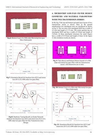
Fig -1: Top (above) and bottom (below) layouts of a fifth
order microstrip low–pass filter with slots under the
transmission lines. (All dimensions are in mm)
Fig -2: Top (above) and bottom (below) Layers of a fifth
order Microstrip low-pass filter (Fabricated).
The first low pass filter design is shown in figure (1) where
there are three apertures in the ground layer. The dimension
in the figure are in mm. In this design the slots were inserted
in ground metallization layer under the low pass filter
transmission line which is in the top layer. In the ground
layer the two side slots have width of 4.9mm and the length
of 3.75 mm. The center slot has width of 4.9mm and length
of 5.65 mm. In Figure 2 the fabricated low pass filter are
shown, it shows the top layer of 5th order filter along with
the bottom layer with three apertures in the ground layer.
The filter designs were tested with the help of SMA
8.0
0
8.0
0
3.7
4.9
5.273 2.85
4.9
3.7
5
4.9
5.6
5
2.85](https://image.slidesharecdn.com/microstriplowpassfilterdesignsusingdefectedgroundstructure-160919071249/85/Microstrip-low-pass-filter-designs-using-defected-ground-structure-2-320.jpg)
![IJRET: International Journal of Research in Engineering and Technology eISSN: 2319-1163 | pISSN: 2321-7308
_______________________________________________________________________________________
Volume: 04 Issue: 10 | Oct-2015, Available @ http://www.ijret.org 45
connectors connected at the input and output of the filters.
Here no transmission zeroes were introduced in the design.
The transmission zeroes are introduced by replacing the
apertures in the ground layer [4]. This leads to the designs
introducing transmission zeroes. Fig. 3 shows the simulation
results for the insertion and return loss of the low-pass filter
without the use of transmission zero design. In the Fig. 3 a
resonance is observed around 7.8 GHz which has as
insertion loss (S21) of -14dB approx. There is another
resonance around 7.9 GHz which has an insertion loss of -
41dB. This design has the pass band insertion loss of -0.1dB
and it matches with the simulation results shown in Fig. 3.
The minimum return loss in the pass band is -13dB. Fig. 4
shows the tested results of the fabricated low pass filter
taken on the Scalar Network Analyzer. The results after
fabrication have proved to be better than the simulation
results. The stop band rejection of the filter are almost same
in the simulated and tested results and the resonance at 7.8
GHz is very low in the tested results compared to the
simulation one. It has maximum insertion loss in the pass
band of -0.43dB. The 2nd harmonic at 6GHz has insertion
loss of -18.74 dB and 3rd harmonic at 9GHz has insertion
loss of -22.22 dB.
Fig -3: Simulation Result for Insertion loss (S21) and return
loss (S11) of a fifth order low-pass filter.
Fig -4: Hardware Testing Results on Scalar Network
Analyzer for Insertion loss (S21) and return loss (S11) of a
fifth order low-pass filter.
3. MICROSTRIP LOW-PASS FILTER DESIGN
GEOMETRY AND MATERIAL PARAMETERS
WITH ONE TRANSMISSION ZERO
To improve the stop band response a one transmission
zero design was introduced in the center slot of ground
layer in the form of interdigital slot structure. The
passband return loss and insertion loss are not affected
but the cut off frequency can be changed by varying
the dimensions of the slot in the form of width and
length. The metal finger has a width of 0.4mm and
length of 3.2mm. The cut off can be shifted back by
reducing the inductance of the narrow line [4],[8]. By
increasing the width of the strip the inductance can be
reduced. The dimensions of the transmission line in
top layer are the same as previous designs. The
fabricated low pass filter design with one transmission
zero is shown in Fig. 6 in which only the bottom layer
with interdigital slots in the middle. Top layer is same
as shown in Fig. 2. The fabricated low pass filter was
tested on Scalar Network Analyzer and its tested
results are shown in Fig. 8. It has maximum insertion
loss in the pass band of -0.46dB. The 2nd harmonic at
6GHz has insertion loss of -21.64 dB and 3rd
harmonic at 9GHz has insertion loss of -21.01 dB.
Fig-5: Top (above) and bottom (below) layouts of a fifth
order microstrip low-pass filter with one transmission zero.
(All dimensions are in mm)
2.85 5.273 2.85
8.0
0
8.0
0
4.9
3.7
5
3.7
5
4.9
3.2
S11
S21
S11
S21](https://image.slidesharecdn.com/microstriplowpassfilterdesignsusingdefectedgroundstructure-160919071249/85/Microstrip-low-pass-filter-designs-using-defected-ground-structure-3-320.jpg)
![IJRET: International Journal of Research in Engineering and Technology eISSN: 2319-1163 | pISSN: 2321-7308
_______________________________________________________________________________________
Volume: 04 Issue: 10 | Oct-2015, Available @ http://www.ijret.org 47
Fig -12: Hardware Testing Results on Scalar Network
Analyzer for Insertion loss (S21) and return loss (S11) of a
fifth order low-pass filter for Two Transmission Zero
Design.
The fabricated low pass filter design with two transmission
zero is shown in Fig. 10 in which only the bottom layer with
interdigital slots at the right and left side are shown. Top
layer is same as shown in Fig. 2. The fabricated low pass
filter was tested on Scalar Network Analyzer and its tested
results are shown in Fig. 12. It has maximum insertion loss
in the pass band of -0.58dB. The 2nd harmonic at 6GHz has
insertion loss of -19.6 dB and 3rd harmonic at 9GHz has
insertion loss of -23.04 dB. Thus harmonics in the stop band
are brought down considerably.
5. CONCLUSION
A fifth order low pass filter was designed and simulated first
and its prototype models were developed. These filters were
designed for the cut off of 3GHz. By properly selecting
impedances of the transmission lines bandwidth of the
broadband low pass filter can be independently designed.
This technical note also introduces interdigital DGS
structure in the slots introduced in the ground layer. The
main advantage of the proposed structures is to get a wide
stop band with a very compact design. You can observe
from the results obtained that the fabricated LPF shows
better results in the stop band behavior than the simulation
results and has stop band rejection of more than 20dB. Thus
a microstrip elliptic low pass filter with a good pass band
return loss and better stop band insertion loss is achieved.
ACKNOWLEDGEMENT
The authors can acknowledge any person/authorities in this
section. This is not mandatory.
REFERENCES
[1]. Ching-Wen Tang and Ming-Guang Chen, “A Microstrip
Ultra-Wideband Bandpass Filter with Cascaded Broadband
Bandpass and Bandstop Filters,” IEEE Transactions On
Microwave Theory and Techniques Vol.55, no.11, pp. 2412-
2418, Nov 2007.
[2]. R A. K. Tiwary, and N. Gupta, "Performance of
Microstrip Low-Pass Filter on Electromagnetic Band Gap
Ground Plane,” IETE Journal of Research, vol.56, Sep-Oct
2010
[3]. Hong-Ming Lee and Ching-Ming Tsai, “Improved
Coupled Microstrip Filter Design Using Effective Even-
mode and Odd-mode Characteristic Impedances,” IEEE
Transactions On Microwave Theory and Techniques Vol.53,
no.9, pp. 2812-2818 ,Sept 2005.
[4] D.D. Gadhvi, S.K. Patel and Yogeshwar Kosta, “Elliptic
Low Pass Filter Design Using DGS Slots for Microstrip
Lines,” 2013 Nirma University International Conference On
Engineering Nuicone-2013, Nov 2013.
[5] A. Balalem, A. R. Ali, J. Machac, Senior Member, IEEE,
and A. Omar, Fellow, IEEE ,"Quasi-Elliptic Microstrip
Low-Pass Filters Using an Interdigital DGS slot," IEEE
Microwave and Wireless Components Letters, pp. 1537-
1309, 2007.
[6] D. K. Mishra, Radio-Frequency and Microwave
Communication Circuits: Analysis and Design,, John Wiley
and sons Inc., pp. 295-353, 2001
[7] Jia-Sheng Hong, M. J. Lancaster ,Microstrip Filters for
RF/Microwave Applications, John Wiley and sons
Inc.,pp.29-76, 2001
[8] S. V. Al-Din Makki, A. Ahmadi, S. Majidifar, H. Sariri,
and Z. Rahmani, "Sharp Response Microstrip LPF using
Folded Stepped Impedance Open Stubs," Radio engineering,
vol.22, no. 1, pp. 328-332, Apr. 2013.
[9]. A. Terado-Mendez, H.Jardon-Aguilar, and R. Flores
Leal, "Improving Frequency Response of Microstrip Filters
using Defected Ground and Defected Microstrip Structures,”
Progress in Electromagnetic Research C, vol. 13, pp. 77-90,
2010.
[10]. Shao Ying Huang and Yee Hui Lee, “Tapered Dual-
Plane Compact Electromagnetic Bandgap Microstrip Filter
Structures,” IEEE Transactions On Microwave Theory and
Techniques Vol.53, no.9, pp. 2656-2664 ,Sept 2005.
[11]. T. Moyra, S. Kumar Parui, and S. Das, "Design and
Development of Low Pass Filter and Harmonics
Reduction,” International Journal on Electrical Engineering
and Informatics, vol. 3, no. 3, pp. 336-349, Oct. 2011.
[12]. L. Wang, H. C. Yang, and Y. Li, "Design Of Compact
Microstrip Low- Pass Filter with Ultra-Wide Stop Band
Using SIRS,” Progress in Electromagnetic Research , vol.
18, pp. 179-186, 2010.
[13]. X. Q. Chen, R. Li, S. J. Shi, Q. Wang, L. Xu, and X.
W. Shi, "A Novel Low Pass Filter Using Elliptic Shape
Defected Ground Structure,” Progress in Electromagnetic
Research B, vol. 9, pp. 117-126, 2008.
[14]. A. Ortega, L. R. A. X. De Menezes, A. J. Martins
Soares, and H. Abdalla Jr., "Design Of Low-Pass Microstrip
Filters Based On Defected Ground Structures,” IEEE MTT-
S International Microwave and Optoelectronics Conference
(IMOC), pp. 69-74, Oct. 2011.
[15]. J. M. Patel, S. K. Patel, and F. N. Thakkar, "Defected
Ground Structure Multiband Microstrip Patch Antenna
Using Complementary Split Ring Resonator,” International
S11
S21](https://image.slidesharecdn.com/microstriplowpassfilterdesignsusingdefectedgroundstructure-160919071249/85/Microstrip-low-pass-filter-designs-using-defected-ground-structure-5-320.jpg)
![IJRET: International Journal of Research in Engineering and Technology eISSN: 2319-1163 | pISSN: 2321-7308
_______________________________________________________________________________________
Volume: 04 Issue: 10 | Oct-2015, Available @ http://www.ijret.org 48
Journal Of Emerging Trends in Electrical and Electronics,
vol. 3, May 2013.
[16]. S. K Patel and Yogeshwar Kosta, “ Triband
Microstrip-Based Radiating Structure Design Using Split
Ring Resonator and Complementary Split Ring Resonator,”
Microwave and Optical Technology Letters, vol. 55, no. 9,
pp. 2219-2222-349, Sept. 2013.
[17]. M. Naser-Moghadasi, R. A. Sadeghzadeh, S. Y. Fard,
and B. S. Virdee, "Microstrip Low-Pass Filters by Using
DGS with Folded T-Shaped Arms,” International Scientific
Publications and Consulting Services, vol.2012, 2012.
[18]. S. Prabhu, J.S. Mandeep and S. Jovanovic, “Microstrip
Bandpass Filter At S Band Using Capacitive Coupled
Resonator,” Progress in Electromagnetic Research B, pp.
223-228, 2007.
[19]. J. Chen, Z.-B. Weng, Y.-C. Jiao and F.-S. Zhang,
“Low Pass Filter Design of Hilbert Curve Ring Defected
Ground Structure,” Progress in Electromagnetic Research B,
pp. 269-280, 2007.
[20]. J. Zhang, B. Cui, S. Lin, and X.-W. Sun, “Sharp-
Rejection Low-Pass filter With Controllable Transmission
Zero Using Complementary Split Ring Resonators
(CSRRS),” Progress in Electromagnetic Research B, pp.
219-226, 2007.
BIOGRAPHIES
Dhara Gadhvi received B.E. degree in 2006
from SVIT, Gujarat and M. Tech degree in
2014 from CSPIT, CHARUSAT university,
Gujarat. Worked as an Electronics Engineer
from 2006 to 2011. Currently working as an
Assistant Professor in Babaria Institute Of
Technology, Gujarat.
Urvik Shah received B.E. degree in 2009
from BVM, Gujarat and M. Tech degree in
2013 from CSPIT, CHARUSAT university,
Gujarat. Currently working as an Assistant
Professor in Babaria Institute Of
Technology, Gujarat.](https://image.slidesharecdn.com/microstriplowpassfilterdesignsusingdefectedgroundstructure-160919071249/85/Microstrip-low-pass-filter-designs-using-defected-ground-structure-6-320.jpg)

The document discusses the design and performance of a fifth order microstrip low pass filter using defected ground structures (DGS) with two different transmission zero configurations. The filters are designed for a cutoff frequency of 3 GHz and show significant improvements in stop band rejection and insertion loss compared to simulation results, achieving over 20 dB of stop band rejection. The study highlights the benefits of incorporating interdigital shapes in DGS for enhanced filter performance in RF/microwave applications.