This document discusses various types of defects that can occur in crystalline solids, including point defects, line defects (dislocations), two-dimensional defects (surfaces and interfaces), and volume defects. It focuses on point defects such as vacancies, interstitials, and solute/impurity atoms. Intrinsic point defects include vacancies and interstitials, while extrinsic defects are caused by solute/impurity atoms. These defects can have significant effects on properties like electrical conductivity in semiconductors and mechanical strength in structural alloys.
The document discusses crystal defects and their significance. It begins with an introduction to crystals and crystal defects. There are four main types of crystal defects discussed: point defects, line defects, surface defects, and volume defects. Point defects include vacancies, interstitials, and impurities. Line defects are dislocations like edge and screw dislocations. Surface defects include grain boundaries, twin boundaries, and stacking faults. Volume defects occur on a larger scale and include voids, porosity, and precipitates. In conclusion, the presence discusses how crystal defects can impact properties and significance like improving semiconductor performance or lowering melting points.
Crystal defects occur when the regular patterns of atoms in crystalline materials are interrupted. There are several types of crystal defects including point defects, line defects, and plane defects. Point defects are defects that occur at or around a single lattice point and include vacancies, interstitials, and substitutions. Vacancies occur when an atom is missing from its normal position in the crystal lattice. Interstitials occur when an atom occupies a position between normal lattice sites. Substitutions occur when a foreign atom replaces a host atom in the lattice. The presence of defects is necessary for crystals to have stability at any non-zero temperature due to the contribution of defects to entropy.
The ideal, perfectly regular crystal structures in which atoms are arranged in a regular way does not exist in actual situations. In actual cases, the regular arrangements of atoms disrupted . These disruptions are known as Crystal imperfections or crystal defects
This document discusses different types of defects in solids. There are two main types of defects - point defects and line defects. Point defects include vacancy defects, where lattice sites are vacant, and interstitial defects, where particles occupy interstitial positions. Point defects in stoichiometric crystals include Schottky defects and Frenkel defects. Non-stoichiometric crystals can have metal excess defects with anionic vacancies or excess cations at interstitial sites, or metal deficient defects with cation vacancies or extra anions at interstitial sites. Impurity defects occur when impurity ions are present at lattice sites or interstitial sites.
Solid state physics (schottkey and frenkel)abi sivaraj
This document discusses different types of lattice defects in crystals. It describes Schottky and Frenkel defects. A Schottky defect occurs in ionic crystals when equal numbers of oppositely charged ions leave their lattice sites, creating vacancies while maintaining overall charge neutrality. A Frenkel defect occurs when an atom moves from its lattice site to an interstitial site, producing a vacancy and interstitial. Schottky defects lower the crystal's density while Frenkel defects do not change density.
There are three main types of point defects in crystals: vacancies, interstitials, and impurities. Line defects include dislocations, which can be edge or screw dislocations. Planar defects involve discontinuities across a plane, such as grain boundaries between differently oriented crystal grains or twin boundaries between mirrored crystal structures. Volume defects create internal surfaces through the absence of atoms in voids.
Imperfections in solids can occur in the form of point defects, line defects, and plane defects. Point defects are irregularities around a single lattice point and include vacancies, interstitial atoms, and displaced atoms. There are different types of point defects based on whether they change the stoichiometry of the solid (stoichiometric defects) or introduce impurities (impurity defects). Stoichiometric defects preserve the overall composition of the solid and include vacancy defects, interstitial defects, Frenkel defects, and Schottky defects in ionic solids. Non-stoichiometric defects change the composition of the solid and lead to metal excess or metal deficiency.
The document provides information about crystal structures, including:
1) It discusses space lattices, which are arrangements of points that repeat periodically in 3D space, with every point having an identical surrounding. The smallest repeating unit of a lattice is called the primitive cell.
2) There are 14 possible crystal structures defined by unique combinations of lattice parameters (a, b, c values and α, β, γ angles). The structures differ in packing efficiency and symmetry.
3) Miller indices are used to specify crystallographic directions and planes, helping to understand properties that vary by orientation like strength and conductivity. Understanding planes and directions is important for predicting deformation and failure modes in materials.
This document discusses various types of imperfections that can occur in crystal structures, including point defects (vacancies, self-interstitials, substitutional impurities), line defects (dislocations like edge and screw dislocations), and planar defects (grain boundaries, twin boundaries, stacking faults). It provides examples of each type of defect, diagrams to illustrate defects like vacancies, interstitials, and different types of dislocations, and brief explanations of defects like Frenkel defects and Schottky defects. The document also mentions defects leading to properties like specific heat and electrical resistance, and discusses concepts like slip and twinning during plastic deformation.
Crystal defects refer to any deviations from the regular geometric arrangement of atoms in a crystal structure. No crystal is truly perfect, as defects are always present due to imperfect packing during crystal formation and thermal vibrations. Common types of defects include vacancies where atomic sites are missing, interstitial defects where extra atoms occupy interstitial spaces, Schottky defects where an anion-cation pair is missing, and Frenkel defects where a cation shifts from its regular site to an interstitial site. Line defects called dislocations are also common, where the crystal structure is distorted along a line, and include edge dislocations from extra atomic planes and screw dislocations from spiral displacements of atoms. Defects significantly
Point defects in solids include vacancies, interstitials, and impurities. Vacancies are vacant atomic sites, while interstitials are atoms that occupy spaces between normal atomic sites. Common point defects include vacancies, self-interstitials, Schottky defects, and Frenkel defects. The concentration of intrinsic point defects like vacancies increases exponentially with temperature based on the energy required to form the defect. Point defects can also create color centers where defects cause colors like the green color from vacancies in diamond.
This document summarizes different types of defects in crystals. It classifies defects as zero-dimensional point defects, one-dimensional line defects, two-dimensional surface defects, or three-dimensional bulk defects. Point defects include vacancies, interstitials, Frenkel defects, and Schottky defects. Line defects include edge and screw dislocations. Surface defects include grain boundaries and twin boundaries. Bulk defects include precipitates, dispersants, inclusions, and voids. Defects can impact material properties and are sometimes deliberately introduced to improve properties.
Properties of coordination compounds part 2 of 3Chris Sonntag
1. Paramagnetism arises from unpaired electrons, which each have their own magnetic moment from both spin and orbital angular momentum.
2. Curie's Law describes how the magnetic susceptibility of a material depends on an external magnetic field and temperature, with higher magnetization occurring at higher fields and lower temperatures.
3. The Curie temperature is the point where a ferromagnetic material loses its permanent magnetism and becomes paramagnetic as spins become randomly oriented with increasing temperature.
- Crystallography is the study of crystalline solids using techniques like X-rays, electron beams, and neutron beams.
- In 1912, Max von Laue proved X-rays were diffracted by crystals, demonstrating diffraction patterns. He received the 1914 Nobel Prize in Physics for this discovery.
- In 1913, father and son team William and Lawrence Bragg developed Bragg's Law to explain X-ray diffraction by crystals and their invention of the X-ray spectroscope earned them the 1914 Nobel Prize in Physics.
This document provides a summary of a lecture on solid state physics. It discusses several key topics:
1. It defines solid state physics as explaining the properties of solid materials by analyzing the interactions between atomic nuclei and electrons within solids.
2. It notes that most solids are crystalline, having a regular repeated atomic structure, and that crystalline solids are easier to analyze than non-crystalline materials.
3. It outlines the lecture, which will cover crystal structures, interatomic forces, and crystal dynamics to explain the behavior and properties of solids.
This document discusses crystal defects and their significance. It begins with an introduction to crystals and crystal defects. There are four main types of crystal defects: point defects, line defects, surface defects, and order-disorder defects. Point defects include vacancy defects, interstitial defects, impurity defects, and non-stoichiometric defects. Line defects cause dislocations like edge and screw dislocations. Surface defects occur at grain boundaries. Order-disorder defects involve random atomic arrangements. Crystal defects are significant as they can influence material properties and enable applications in areas like semiconductors, lowering melting points, and nanotube growth. In conclusion, no crystal is perfect and defects are usually present and often useful.
Crystal defects impact the properties of crystalline materials. Point defects are irregularities around a single atom, such as vacancies where an atom is missing or interstitials where an extra atom is present. Line defects include dislocations where the ordered atomic planes are disturbed along a line. Surface defects occur at boundaries between regions with different crystal structures. Bulk defects are larger precipitates, inclusions, or voids within the material volume. Defects are classified based on their dimensionality and can be intentionally introduced to modify material properties.
This document summarizes different types of defects in solids, including intrinsic and extrinsic defects. It discusses point defects like vacancies and impurities, as well as line defects. Intrinsic defects such as Schottky and Frenkel defects are thermally created and do not depend on impurity concentrations. Extrinsic defects can be introduced intentionally through doping with aliovalent ions, which preserves electroneutrality but creates vacancies. Examples given include adding CaCl2 to KCl to replace two K+ ions with one Ca2+ ion, creating a cation vacancy. Overall, the document provides an overview of different defect types in solids and how intrinsic defects differ from extrinsic defects introduced through doping.
This document discusses different types of crystal defects. It begins by defining an ideal crystal and explaining that real crystals contain defects due to deviations from a completely ordered atomic arrangement. Crystal defects are classified as point defects, line defects, planar defects, or bulk defects depending on their geometry. Point defects, which occur around a single atom, are further divided into vacancy defects, interstitial defects, Schottky defects, and Frenkel defects. Line defects include edge dislocations and screw dislocations. Planar defects involve grain boundaries and stacking faults, while bulk defects are voids, cracks, or impurity inclusions. The document provides examples and descriptions of each type of defect.
[1] Crystal defects are irregularities in the structure of a crystal that arise from imperfect packing of atoms. There are several types of crystal defects including point defects, line defects, surface defects, and volume defects.
[2] Point defects are zero-dimensional and include vacancies, interstitial defects, Schottky defects, and Frenkel defects. Line defects are one-dimensional and include edge and screw dislocations. Surface defects are two-dimensional and include grain boundaries, twin boundaries, and stacking faults. Volume defects are three-dimensional voids or non-crystalline regions within the crystal structure.
Crystal imperfections are broadly classified into four categories: point defects, line defects, planar/surface defects, and volume defects. Point defects include vacancies, interstitials, and impurities which lower the crystal's energy and make it more stable. Line defects are dislocations which are line discontinuities in the crystal structure. Planar defects include grain boundaries, tilt boundaries, and twin boundaries which separate regions of different crystal orientation. Volume defects such as stacking faults disrupt the ordered stacking of close-packed crystal planes. Defects can be either desirable by improving material properties, or undesirable if they reduce properties.
The document discusses different types of crystal defects including point defects, stoichiometric defects, and non-stoichiometric defects. Stoichiometric defects include Schottky and Frenkel defects which involve cation-anion pairs missing or cation dislocations. Non-stoichiometric defects result from deviations from the ideal ratio of cations to anions and include metal excess or deficiency defects involving anion or cation vacancies. Common examples of different defect types in various crystals are provided.
This document discusses various types of defects that can occur in crystalline solids. It defines point defects as defects involving a few extra or missing atoms located at or near a single lattice point. The main types of point defects discussed are vacancies, where an atom is missing from its site; interstitials, where atoms occupy spaces between normal lattice sites; and substitutions, where one atom replaces another. It also describes Frenkel defects, where an atom moves from its normal site to an interstitial site, and Schottky defects, which involve vacancies of oppositely charged ions in ionic crystals to maintain neutral charge. These defects influence properties like ion transport and electrochemical reactions in solids.
Crystals are composed of repeating unit cells that generate the entire crystal structure when translated through space. A crystal's symmetry is defined by symmetry elements like rotations, translations, and reflections that leave the crystal unchanged. There are 32 possible point groups and 14 Bravais lattices that combine to form 230 unique space groups describing all possible crystal symmetries. The asymmetric unit is the smallest portion of the unit cell that generates the full crystal structure through symmetry operations.
Solids are characterized by their definite shape and also their considerable mechanical strength and rigidity. The particles that compose a solid material(with few exceptions), whether ionic, molecular, covalent or metallic, are held in place by strong attractive forces between them.
This document discusses spinels and inverse spinels, which are metal oxides with general formulas of AB2X4 and (BIII)tet(AIIBIII)octX4 respectively. Spinels have a normal cubic close-packed structure with B3+ ions occupying half the octahedral holes and A2+ ions occupying one-eighth of the tetrahedral holes. Examples include MgAl2O4 and Mn3O4. Inverse spinels have an alternate arrangement with A2+ ions occupying the octahedral voids and half of B3+ ions occupying the tetrahedral voids. The document also discusses perovskites, which have the general formula ABX3 and examples include barium
In the vast realm of materials science, vacancy defects are microscopic imperfections that play a significant role in shaping the properties and behavior of solid materials. Vacancies, also known as point defects, occur when atoms or ions are missing from their expected positions within the crystal lattice. Despite their seemingly small size, these vacancies have profound implications on material properties, such as density, electrical conductivity, and diffusion rates. In this article, we will explore the intriguing world of vacancy defects in solids, examining their formation, effects, and their relevance in various applications.
The document discusses various types of defects that can occur in crystalline materials, including point defects like vacancies and self-interstitials, and linear defects like dislocations. It explains that all crystals contain vacancies which increase with temperature according to an exponential relationship. Dislocations are line defects characterized by their Burgers vector, and can be either edge, screw, or mixed configurations. Interfacial defects like grain boundaries separate regions with different crystal orientations. These defects influence many material properties.
Mumbai University_Mechanical Enginnering_SEM III_ Material technology_Module 1.2
Lattice Imperfections:
Definition, classification and significance of Imperfections Point defects: vacancy, interstitial and impurity atom defects, Their formation and effects, Dislocation - Edge and screw dislocations Burger’s vector, Motion of dislocations and their significance, Surface defects - Grain boundary, sub-angle grain boundary and stacking faults, their significance, Generation of dislocation, Frank Reed source, conditions of multiplication and significance
This document discusses different types of crystalline defects including point defects, linear defects, and interfacial defects. It describes point defects as vacancies where an atom is missing from its lattice site or as self-interstitials where an atom occupies an interstitial void space. Impurities are also considered point defects when added to alloys to impart specific material properties. Linear defects called dislocations are discussed as one-dimensional defects where some atoms are misaligned around an extra half-plane of atoms. Dislocations can be in the form of an edge dislocation along the end of the extra half-plane or a screw dislocation involving a shear distortion of the crystal structure.
This document discusses different types of point defects that can occur in crystalline solids. There are three main types of point defects: 1) Stoichiometric defects include vacancies where an atom is missing from its lattice site, and interstitials where an atom occupies an interstitial space in the lattice. 2) Frenkel defects occur when a smaller cation moves from its lattice site into an interstitial space, creating both a vacancy and interstitial. 3) Schottky defects occur in ionic solids and involve an equal number of cation and anion vacancies to maintain charge neutrality, reducing the material's density.
There are several types of defects that can occur in crystalline materials, including point defects, line defects, and grain boundaries. Point defects include vacancies, interstitial atoms, and substitutional/interstitial impurities. Line defects include stacking faults which occur when the regular stacking sequence of atomic planes is disturbed. Grain boundaries separate crystalline grains of different orientations in polycrystalline materials. These defects influence many properties of materials.
In the realm of materials science, cation vacancies are intriguing imperfections that disrupt the perfect arrangement of atoms within solid materials. Cation vacancies occur when positively charged ions, known as cations, are missing from their expected positions within the crystal lattice. These vacancies introduce localized regions of charge imbalance, impacting material properties such as electrical conductivity, thermal behavior, and mechanical properties. In this article, we will delve into the captivating world of cation vacancies in solids, exploring their formation, effects on material properties, and their relevance in various applications.
This document discusses various types of defects that can occur in crystalline materials. It describes four main categories of defects: point defects, surface defects, line defects, and volume defects. Point defects include vacancies, interstitial defects, and impurity substitutions. Specific point defects discussed for ionic solids include Frenkel and Schottky defects. Stacking faults are described as planar defects that disrupt the regular stacking sequence of atomic layers. Grain boundaries are also discussed as planar defects that separate crystalline regions with different orientations within polycrystalline materials.
CBSE Class 12 Chemistry Chapter 1 (The Solid State) | Homi InstituteHomi Institute
The document discusses various types of bonding and intermolecular forces found in solid state materials, including covalent bonding, metallic bonding, ionic bonding, hydrogen bonding, and van der Waals forces. It also describes different types of crystal defects such as point defects, line defects, stoichiometric defects, impurity defects, and non-stoichiometric defects. Finally, it covers topics like semiconductors, ferromagnetism, and the magnetic properties associated with orbiting and spinning electrons.
In the realm of materials science, the study of point defects is crucial for understanding the intricate world of solid materials. Point defects, also known as lattice defects, are atomic-level imperfections that occur within the crystal lattice of a solid. These microscopic deviations from the ideal crystal structure play a significant role in determining the properties and behavior of materials. In this article, we will delve into the fascinating realm of point defects in solids, exploring their types, formation mechanisms, and impact on material properties.
There are several types of imperfections or defects that can occur in crystal structures including point defects, line defects, interfacial defects, and bulk defects. Point defects include vacancies and interstitials which occur naturally in all crystals. Line defects are imperfections where rows of atoms have a differing structure, such as dislocations. Interfacial defects include grain boundaries and twin boundaries. The number and type of defects can be controlled and affect material properties, both positively and negatively.
In the realm of materials science, the study of crystal defects is an intriguing and critical field. While crystals are renowned for their remarkable structural order and perfection, they are not exempt from imperfections. Crystal defects, also known as lattice defects, are deviations from the ideal arrangement of atoms or ions within a crystal lattice. These defects can have profound implications on the properties and behavior of materials, making their exploration and understanding crucial for various scientific and technological advancements. In this article, we will delve into the world of crystal defects, their classification, and their impact on solid materials.
In the fascinating world of materials science, understanding the different types of defects is crucial to unraveling the mysteries of solid materials. Defects, or imperfections, are inherent to the structure of materials and can greatly influence their properties and behavior. By classifying and studying these defects, scientists and engineers can gain valuable insights that drive advancements in fields such as manufacturing, electronics, and materials design. In this article, we will explore the various types of defects found in solid materials and their significance in different applications.
This document discusses different types of lattice disorder in crystalline solids. It describes four main types of lattice disorder: point disorder, line disorder, planar disorder, and bulk disorder. Point disorder occurs at single lattice points and includes vacancies, interstitials, Frenkel defects, substitutional defects, and antisite defects. Line disorders include edge dislocations and screw dislocations. The document provides examples and explanations of each type of lattice disorder.
This document discusses various types of crystal defects including point defects, line defects, and planar defects. It defines point defects as zero-dimensional defects involving a single atom change, such as vacancies, interstitials, and impurities. Line defects are described as one-dimensional dislocations, including edge and screw dislocations. Planar defects are two-dimensional grain boundaries that separate crystalline regions with different orientations within a polycrystalline solid. The document explores how these defects influence material properties.
In the realm of materials science, interstitial defects are remarkable imperfections that introduce new elements into the crystal lattice of solids, leading to significant modifications in material properties. Interstitial defects occur when foreign atoms or ions occupy the spaces between regular lattice sites. Despite their small size, these interstitials can have profound effects on material characteristics such as mechanical strength, electrical conductivity, and diffusion rates. In this article, we will delve into the intriguing world of interstitial defects in solids, exploring their formation, impact on material properties, and their relevance in various applications.
Complete notes on crystal defects provided to you by JFC (A place where you feel the chemistry). For all boards, competition like NET(JRF), GATE, NEET, IIT (JEE) ....
Crystal defects can be classified based on their geometry. Point defects are zero-dimensional and include vacancies, interstitials, and impurities. Line defects are one-dimensional dislocations such as edge and screw dislocations. Surface defects are two-dimensional and include grain boundaries and stacking faults. Volume defects are three-dimensional such as cracks, voids, and inclusions. Real crystals always contain imperfections that influence material properties. Understanding crystal defects is important for both analyzing material behavior and developing techniques to minimize their impact.
Defects are common in real crystals and influence their properties. Point defects include vacancies, interstitials, and impurities. Line defects are dislocations like edge and screw dislocations. The type and amount of defects can be controlled to alter electrical, thermal, and mechanical properties in beneficial ways like improving semiconductor performance or alloy strength. Defects are characterized by their geometry and the Burgers vector, which describes the crystal distortion caused by a dislocation.
This document provides an overview of fuse characteristics, terms, considerations, and selection factors. It defines key fuse-related terms like current rating, breaking capacity, dimensions, and construction. It also covers selection factors like ambient temperature, pulses, and standards. The purpose is to help readers understand fuses and properly select the right fuse for their application. Selection involves considering characteristics like operating current, temperature, pulses and standards to avoid issues like nuisance opening.
Robotics and control theory have a long history of interaction, with each field helping to advance the other. Early industrial robots had independent joint control without sensing, but consideration of tasks like assembly required new control methods. Developments in nonlinear, robust, and adaptive control enabled more sophisticated robot applications. Today, advances in computation, sensors, and networking have led to applications like mobile robots, surgical robots, and robot networks playing increasing roles in society. Key challenges going forward include control of underactuated, legged, and multi-agent robotic systems.
A microprocessor is an integrated circuit designed to function as the CPU of a microcomputer. It reads instructions from memory, decodes and executes them, and processes data as required. The microprocessor incorporates various functional units like an ALU, registers, instruction decoder, and control unit. It communicates with external memory and I/O devices via address, data, and control buses. Memory is used to store both instructions and data, and comes in RAM and ROM varieties. Interfaces are needed to connect peripherals to the microprocessor and handle functions like buffering, addressing decoding, and timing/control of data transfers. Software for microprocessors includes machine language programs and programs written in assembly/high-level languages which are
The document describes how to set up and use a Michelson interferometer to study the interference of light waves. Key steps include:
1. Aligning a diode laser, beam splitter, and two mirrors on an optical breadboard to split and recombine the laser light.
2. Using the interference fringes formed to calibrate the sub-micrometer movement of one of the mirrors and determine the laser wavelength.
3. Observing how the contrast of the interference fringes is affected by the path difference between the light beams and their relative plane of polarization.
This document discusses superposition and standing waves. It covers topics such as constructive and destructive interference, resonant modes of systems, and beats. Examples are provided of superposition and interference. Standing waves on strings are discussed, including the different harmonic modes that are produced from varying the wavelength using the same string length. Higher harmonics produce higher pitches. Factors like tension and mass density that affect the pitch of string instruments are also covered.
The document summarizes key discoveries and concepts in superconductivity research. It describes:
1) The discovery of superconductivity by Kamerlingh Onnes in 1911 when studying the resistance of mercury at low temperatures.
2) The Meissner effect discovered in 1933 showing that superconductors expel magnetic fields.
3) The distinction between type I and type II superconductors based on their behavior in magnetic fields. Type II are more useful for applications.
4) BCS theory from 1957 explaining superconductivity through the formation of electron pairs called Cooper pairs experiencing attractive interactions.
5) The discovery of high-temperature superconductors in 1986 with critical temperatures accessible using liquid
This document provides an introduction to alloy phase diagrams. It discusses how alloy phase diagrams are useful for metallurgists in developing new alloys, processing alloys, and solving performance issues. The document then defines key terms related to alloy phase diagrams including phases, equilibrium, polymorphism, metastable phases, systems, phase diagrams, and the phase rule. It provides examples of unary, binary, and ternary phase diagrams. Specifically, it discusses invariant equilibrium, univariant equilibrium, and bivariant equilibrium for unary systems. It also discusses miscibility in solid and liquid states, liquidus and solidus lines, eutectic reactions, and three-phase equilibrium for binary systems.
This document provides instructions for configuring and using the frequency counter feature of the Midnight Scalar Network Analyzer (MSNA). It discusses how frequency measurements are made, how to tune the timing functions for better accuracy, and describes an optional RF signal conditioning circuit. Calibration of the frequency counter involves coarse adjustment of the system clock frequency and fine adjustment of the counting period to accurately measure signals from a precision frequency source like a 10 MHz reference.
This document provides information on various electrical measuring instruments produced by Iskra MIS, including measuring centers, transducers, communication adapters, meters, and accessories. It describes the features and specifications of different product lines for measuring voltage, current, power, energy, harmonics and more. The measuring centers can measure over 60 electrical quantities and record data, with models for permanent network analysis and quality evaluation according to standards.
1) Cubic equations can have one real root or three real roots. They always have at least one real root.
2) Cubic equations can be solved by using synthetic division to reduce them to a quadratic equation if one root is known, or by spotting factors.
3) Graphs of cubic equations cross the x-axis at least once, showing they have at least one real root, and can help locate approximate solutions.
The document provides information on basic first aid steps and procedures. It outlines the DRSABCD action plan for responding to emergencies, which stands for Danger, Response, Send for help, Airway, Breathing, Compressions, and Defibrillation. The document also describes how to treat common first aid situations like bleeding, burns, head injuries, seizures, fractures, choking, and heatstroke. It emphasizes the importance of first aid training and knowing what to do in emergency situations.
This document discusses some of the key issues, challenges, and opportunities related to the field of engineering and human development. It notes that while engineering has helped provide basic needs like water, food, shelter and energy to society, it has also contributed to increases in weapons destruction, inequality, and environmental damage. Specifically, it points out that the lethality of weapons, military spending, and pollution from fossil fuel use have all dramatically increased over time due to engineering advances. However, it also acknowledges that engineering plays an important role in addressing problems like providing health systems, education access, and tackling climate change and environmental issues. The document argues that the engineering profession could do more to maximize its positive contributions to society and minimize harm, such
Engineering has both positive and negative impacts on society. Positively, engineering provides basic needs like water, food, shelter and energy, improving lives globally. However, engineering has also enabled huge increases in weapons destruction over centuries and contributes to issues like pollution, climate change and species loss. As technology grows more complex and society depends on it more, failures or misuse also pose greater risks. Responsible engineering requires understanding these dual impacts and maximizing benefits while mitigating harm.
Exploiting Artificial Intelligence for Empowering Researchers and Faculty, In...Dr. Vinod Kumar Kanvaria
Exploiting Artificial Intelligence for Empowering Researchers and Faculty,
International FDP on Fundamentals of Research in Social Sciences
at Integral University, Lucknow, 06.06.2024
By Dr. Vinod Kumar Kanvaria
Strategies for Effective Upskilling is a presentation by Chinwendu Peace in a Your Skill Boost Masterclass organisation by the Excellence Foundation for South Sudan on 08th and 09th June 2024 from 1 PM to 3 PM on each day.
Walmart Business+ and Spark Good for Nonprofits.pdfTechSoup
"Learn about all the ways Walmart supports nonprofit organizations.
You will hear from Liz Willett, the Head of Nonprofits, and hear about what Walmart is doing to help nonprofits, including Walmart Business and Spark Good. Walmart Business+ is a new offer for nonprofits that offers discounts and also streamlines nonprofits order and expense tracking, saving time and money.
The webinar may also give some examples on how nonprofits can best leverage Walmart Business+.
The event will cover the following::
Walmart Business + (https://business.walmart.com/plus) is a new shopping experience for nonprofits, schools, and local business customers that connects an exclusive online shopping experience to stores. Benefits include free delivery and shipping, a 'Spend Analytics” feature, special discounts, deals and tax-exempt shopping.
Special TechSoup offer for a free 180 days membership, and up to $150 in discounts on eligible orders.
Spark Good (walmart.com/sparkgood) is a charitable platform that enables nonprofits to receive donations directly from customers and associates.
Answers about how you can do more with Walmart!"
it describes the bony anatomy including the femoral head , acetabulum, labrum . also discusses the capsule , ligaments . muscle that act on the hip joint and the range of motion are outlined. factors affecting hip joint stability and weight transmission through the joint are summarized.
How to Add Chatter in the odoo 17 ERP ModuleCeline George
In Odoo, the chatter is like a chat tool that helps you work together on records. You can leave notes and track things, making it easier to talk with your team and partners. Inside chatter, all communication history, activity, and changes will be displayed.
A workshop hosted by the South African Journal of Science aimed at postgraduate students and early career researchers with little or no experience in writing and publishing journal articles.
This slide is special for master students (MIBS & MIFB) in UUM. Also useful for readers who are interested in the topic of contemporary Islamic banking.
How to Fix the Import Error in the Odoo 17Celine George
An import error occurs when a program fails to import a module or library, disrupting its execution. In languages like Python, this issue arises when the specified module cannot be found or accessed, hindering the program's functionality. Resolving import errors is crucial for maintaining smooth software operation and uninterrupted development processes.
BÀI TẬP BỔ TRỢ TIẾNG ANH 8 CẢ NĂM - GLOBAL SUCCESS - NĂM HỌC 2023-2024 (CÓ FI...
Defects
1. Materials Science J.W. Morris, Jr.
Page 76
Chapter 4: Defects in Cr ystalsChapter 4: Defects in Cr ystals
...Perfection's a gift of
The gods, few can boast they possess it - and most
Of you, my dears, don't.
- Ovid, The Art of Love
Chapter 4: Defects in Crystals ............................................................................................ 76
4.1 Introduction.................................................................................................... 76
4.2 Point Defects .................................................................................................. 77
4.2.1 Intrinsic defects ............................................................................... 77
4.2.2 Extrinsic defects .............................................................................. 78
4.3 Line Defects: Dislocations ............................................................................ 83
4.3.1 The edge dislocation ....................................................................... 83
4.3.2 An edge dislocation in a simple cubic crystal ............................... 86
4.3.3 The Burgers circuit.......................................................................... 88
4.3.4 Motion of an edge dislocation: glide and climb............................ 88
4.3.5 Screw dislocations........................................................................... 90
4.3.6 Screw dislocations and plastic deformation .................................. 91
4.3.7 Dislocations in real materials: mixed dislocations........................ 91
4.3.8 Partial dislocations .......................................................................... 93
4.4 Two-Dimensional Defects: Interfaces.......................................................... 96
4.4.1 Free surfaces.................................................................................... 96
4.4.2 Interfaces between crystals............................................................. 99
4.4.3 Interfaces within crystals ................................................................ 104
4.5 Volume Defects ............................................................................................. 106
4.1 INTRODUCTION
A perfect crystal is an idealization; there is no such thing in nature. Atom
arrangements in real materials do not follow perfect crystalline patterns. Nonetheless,
most of the materials that are useful in engineering are crystalline to a very good approxi-
mation. There is fundamental physical reason for this. The preferred structures of solids
at low temperature are those that minimize the energy. The low-energy atomic
configurations are almost invariably crystalline since the regular pattern of the crystal
lattice repeats whatever local configuration is most favorable for bonding. There is also a
fundamental physical reason why the crystal is imperfect. While a perfect crystalline
structure may be preferred energetically, at least in the limit of low temperature, atoms
are relatively immobile in solids and it is, therefore, difficult to eliminate whatever
imperfections are introduced into the crystal during its growth, processing or use.
2. Materials Science J.W. Morris, Jr.
Page 77
The fact that real materials are not perfect crystals is critical to materials engi-
neering. If materials were perfect crystals then their properties would be dictated by their
composition and crystal structure alone, and would be very restricted in their values and
their variety. It is the possibility of making imperfectly crystalline materials that permits
materials scientists to tailor material properties into the diverse combinations that modern
engineering devices require. As we shall see repeatedly in the body of this course, the
most important features of the microstructure of an engineering material are the
crystalline defects that are manipulated to control its behavior.
In this Chapter we shall identify and describe the various defects that are found in
crystalline solids. We shall hint at their consequences to indicate why they are worth
studying, but shall defer a detailed discussion of their behavioral role until we discuss
particular classes of engineering properties.
It is useful to classify crystal lattice defects by their dimension. The 0-
dimensional defects affect isolated sites in the crystal structure, and are hence called point
defects. An example is a solute or impurity atom, which alters the crystal pattern at a
single point. The 1-dimensional defects are called dislocations. They are lines along
which the crystal pattern is broken. The 2-dimensional defects are surfaces, such as the
external surface and the grain boundaries along which distinct crystallites are joined
together. The 3-dimensional defects change the crystal pattern over a finite volume.
They include precipitates, which are small volumes of different crystal structure, and also
include large voids or inclusions of second-phase particles.
4.2 POINT DEFECTS
A point defect disturbs the crystal pattern at an isolated site. It is useful to distin-
guish intrinsic defects, which can appear in a pure material, from extrinsic defects, which
are caused by solute or impurity atoms.
4.2.1 Intrinsic defects
An intrinsic defect is formed when an atom is missing from a position that ought
to be filled in the crystal, creating a vacancy, or when an atom occupies an interstitial site
where no atom would ordinarily appear, causing an interstitialcy. The two types of
intrinsic point defects are shown in Fig. 4.1.
3. Materials Science J.W. Morris, Jr.
Page 78
vacancy
interstitialcy
Fig. 4.1: Illustration of a vacancy and an interstitial in a two-dimensional
hexagonal lattice.
Because the interstitial sites in most crystalline solids are small (or have an
unfavorable bonding configuration, as, for example, in the diamond lattice) interstitialcies
are high-energy defects that are relatively uncommon. Vacancies, on the other hand, are
present in a significant concentration in all crystalline materials. Their most pronounced
effect is to govern the migration of atoms on the crystal lattice (solid state diffusion). In
order for an atom to move easily from one crystal lattice site to another the target site
must be vacant. As we shall see, the rate of diffusion on the crystal lattice is largely
governed by the concentration of vacancies.
Ordered compounds can have more complex intrinsic defects. In most
compounds the different species are charged to at least some degree. An intrinsic defect
destroys the local charge balance, which must be restored in some way. The compound
defects that preserve charge are easiest to visualize in binary ionic solids like NaCl. An
isolated vacancy in an ionic solid creates an excess charge. The excess charge can be
compensated by a paired vacancy on the sublattice of the other specie; for example, the
excess charge associated with a Na vacancy is balanced if there is a Cl vacancy nearby.
A neutral defect that involves paired vacancies on the cation and anion sublattices is
called a Schottky defect. Alternatively, the charge imbalance caused by the vacancy can
be corrected by adding an interstitial of the same specie; a Na vacancy is compensated by
a Na interstitial. A neutral defect that is made up of a paired vacancy and interstitial is
called a Frenkel defect. In compounds whose atoms are less strongly ionized it is
energetically possible for species to exchange sites, so that an A-atom appears on the B-
sublattice or vice versa. This type of point defect is called an anti-site defect, and is fairly
common in semiconducting compounds such as GaAs.
4.2.2 Extrinsic defects
The extrinsic point defects are foreign atoms, which are called solutes if they are
intentionally added to the material and are called impurities if they are not. The foreign
atom may occupy a lattice sites, in which case it is called a substitutional solute (or impu-
rity) or it may fill an interstitial site, in which case it is called an interstitial solute. Since
the interstitial sites are relatively small, the type of the solute is largely determined by its
4. Materials Science J.W. Morris, Jr.
Page 79
size. Small atoms, such as hydrogen, carbon and nitrogen are often found in interstitial
sites. Larger atoms are usually substitutional.
More complex extrinsic defects appear in compounds. If the valence of a
substitutional defect in an ionic solid differs from that of the lattice ion then the excess
charge is often compensated by a paired vacancy or interstitial. For example, when Mg++
ions are substituted for Na+ in NaCl they tend to be paired with vacancies on the Na
sublattice to maintain local charge neutrality. In semiconductors substitutional atoms
with the wrong valence acts as electron donors or acceptors, as described below.
Extrinsic point defects affect almost all engineering properties, but they are
particularly important in semiconducting crystals, where extrinsic defects are used to
control electrical properties, and in structural metals and alloys, where extrinsic defects
are added to increase mechanical strength. While these properties will be discussed later
in the course, it is perhaps useful to identify the characteristics of the point defects that
affect them.
Donors and acceptors in semiconductors
Point defects are intentionally added to semiconductors to control the type and
concentration of charge carriers. Consider, for example, boron (valence 3) as a substi-
tutional solute in elemental silicon. The saturated covalent bonds in silicon are shown
schematically in Fig. 4.2a, and depend on the availability of four valence electrons per
silicon atom. Since the bonds are saturated, silicon has very low conductivity in its pure
state; pure silicon can only conduct electricity when electrons are excited into high-
energy electron states. If boron is added, as in Fig. 4.2b, a valence electron is missing
from the immediate environment of the boron atom, causing a hole in the bonding
pattern. Electrons can then move from bond to bond by exchanging with the hole. The
exchange requires some energy to separate the hole from the boron ion core, but this
energy is small compared to that required to excite an electron from a Si-Si bond into a
high-energy state. The room-temperature conductivity of Si increases significantly when
a small amount of B is added. Electron-deficient solutes like boron that cause holes in
the configuration of bonding electrons are called acceptors.
Si
Si
Si
Si
Si
Si
Si
Si
Si
B
Si
Si
Si
Si
P
e
(a) (b) (c)
Fig. 4.2: (a) Tetrahedral bonding configuration in Si. (b) Bonding around
a B solute, showing a hole ( ). (c) Bonding around a P solute,
showing an electron (e) in a loose excited orbital.
5. Materials Science J.W. Morris, Jr.
Page 80
The conductivity also rises when a solute with an excess of electrons is added to a
semiconductor with saturated bonds. For example, let phosphorous (valence 5) be added
to Si, as in Fig. 4.2c. The 5 valence electrons of P are sufficient to fill the local covalent
bonds with one electron left over. This electron can only go into an excited state, and or-
bits about the P ion core somewhat as shown in the figure. It requires a relatively small
energy increment to free this electron from the P core, in which case it can transport
current by moving through the lattice. The conductivity of Si rises dramatically if a small
amount of P is added. Electron-excess solutes such as P in Si are called donors.
Semiconductors whose electrical properties are controlled by electrically active
solutes are called extrinsic semiconductors. Almost all of the semiconductors that are
used in engineering devices are extrinsic.
Solution hardening in structural materials
The addition of solute atoms almost always increases the mechanical strength of a
solid. The phenomenon is called solution hardening. It is due to the fact that the solute
atom is always a bit too large or a bit too small to fit perfectly into the crystal lattice site
it is supposed to occupy, and distorts the crystal lattice in its attempt to fit as well as
possible. As we shall see later, this distortion impedes the motion of the linear defects
(dislocations) that are responsible for plastic deformation and, consequently, hardens the
crystal. The distortion due to a substitutional solute is relatively small, though the
associated hardening may be large enough to be useful in the engineering sense. The
distortions due to interstitial atoms such as carbon and nitrogen are normally much
greater because of the small size of the interstitial void in which they must fit. The
hardening effect of interstitial solutes is large and technologically important; for example,
high strength structural steels are alloys of Fe and C.
There is a simple crystallographic reason why interstitial solutes such as C are
particularly effective in strengthening BCC metals such as Fe. The carbon atoms occupy
octahedral interstitial sites in the BCC structure Since an atom in an octahedral void in
BCC is closer to two of its neighbors that to the other four, it causes an asymmetric
distortion of the lattice. As shown in Fig. 4.3, the octahedron is stretched along its short
axis, which is the a3, or z-axis in the case shown in the figure. The asymmetric distortion
of the interstitial site increases its interaction with the dislocations that cause plastic
deformation and promotes hardening. In FCC alloys the interstitial sites are symmetric,
and the lattice distortion is isotropic. Interstitial solutes are effective in hardening FCC
alloys, but are less effective than in BCC alloys.
6. Materials Science J.W. Morris, Jr.
Page 81
Fig. 4.3: The local distortion of the BCC lattice by an interstitial atom in
an Oz void.
Random solid solutions
At low concentrations it is usually reasonable to assume that the solutes are ran-
domly distributed over the sites they occupy, in which case the material is called a
random solid solution. The basic properties of a random substitutional solid solution can
often be estimated by treating the material as if it were made up of pseudo-atoms that
have the average properties of the components of the solution. In keeping with this idea,
most of the properties of random substitutional solid solutions are simply proportional to
the solute concentration. We shall see many examples in the following. A particular
example is Vegard's Law, which asserts that when the solute concentration in a cubic
solid solution is small its lattice parameter changes linearly with the concentration:
a - a0
a0
= Kx 4.1
where a0 is the lattice parameter of the crystal in pure form, x is the atom fraction of
solute and K is a constant. The constant, K, is usually much larger for an interstitial
solute because the solute atom must be fit into the small interstitial hole.
Tetragonal distortion by octahedral interstitials in BCC
At larger solute concentrations the solute atoms interact and influence one
another, and their actual configuration in the crystal becomes important. An important
and instructive example occurs in the case of octahedral interstitials in BCC materials,
and is responsible for the technologically important fact that steel (Fe-C) that has a
carbon content greater than a few tenths of an atom percent has a body-centered
tetragonal rather than a BCC structure when it cooled rapidly (quenched) from elevated
temperature. The body-centered tetragonal structure (BCT) differs from the BCC in that
it is elongated along one of the three crystal axes (assume the a3, or z-axis), as shown in
Fig. 4.4.
7. Materials Science J.W. Morris, Jr.
Page 82
a1
a2
a3
Fig. 4.4: Tetragonal distortion of a cube. the distortion creates a
tetragonal figure with an increased value of |a3|.
The source of the BCT structure lies in the asymmetry of the octahedral void that
is the preferred site for carbon. Since there are equal numbers of Ox, Oy and Oz octahedra
in the BCC lattice, a random distribution of octahedral interstitials causes, on the average,
an equal distortion of the three crystal axes and simply expands the BCC lattice.
However, because of the asymmetric distortion, octahedral interstitials interact with one
another and, if they are present in any significant concentration, preferentially occupy one
of the three types of octahedral sites so that their short axes are aligned. When this
happens there is a net long-range distortion of the crystal lattice in the direction of the
short axis of the interstitial void that changes the structure from BCC to BCT.
When pure Fe is cooled from high temperature its structure changes from FCC to
BCC. Carbon is more soluble in the FCC phase. If an FCC Fe-C alloy with a moderate
carbon content is cooled very rapidly (quenched) then the carbon is trapped in the BCC
product. The carbon interstitials preferentially adopt aligned octahedral sites, with the
consequence that the quenched alloy, which is called martensite, has a body-centered
tetragonal (BCT) structure. It is a very strong material with many important uses.
Decomposition and ordering of solid solutions
Very few species are mutually soluble in all proportions. The solubility range is
ordinarily limited by the preferential interaction of the solute atoms, and is limited in one
of two ways. If the solute atoms bond preferentially to one another they tend to become
associated in the solid solution, or cluster. As the concentration of solute increases the
tendency to cluster becomes more pronounced, until the solution spontaneously
decomposes into a mixture of two solutions, or phases, one of which is rich in the solute
and one in the solvent. The point at which this decomposition occurs defines the
solubility limit of the solid solution. On the other hand, if the solute atoms bond
preferentially to the solvent then they tend to adopt ordered configurations in which
solute and solvent alternate in a regular crystal pattern. When the solute concentration
becomes great enough the solution decomposes into a mixture of a solution that is rich in
solvent and an ordered compound that contains nearly stoichiometric proportions of the
two atom types.
8. Materials Science J.W. Morris, Jr.
Page 83
Note that the definition of a point defect in an ordered compound of species A and
B is different from that in a solid solution of B in A. A point defect in a compound is a
deviation from the perfectly ordered state of the compound structure. For example, in a
solid solution of Au in Cu each Au atom constitutes a point defect, since the pure Cu
crystal is the reference. In the intermetallic compound Cu3Au, on the other hand, an Au
atom is a point defect only if it occupies a Cu position in the Cu3Au structure (in which
case it is an anti-site defect), while a Cu atom is a point defect if it occupies an Au site.
This re-emphasizes the important point that a "crystal defect" is a deviation from the
configuration the crystal would have if it were perfectly ordered, and has no meaning
until the reference state, the perfectly ordered crystal, is defined.
4.3 LINE DEFECTS: DISLOCATIONS
Dislocations are linear defects; they are lines through the crystal along which
crystallographic registry is lost. Their principle role in the microstructure is to control the
yield strength and subsequent plastic deformation of crystalline solids at ordinary
temperatures. Dislocations also participate in the growth of crystals and in the structures
of interfaces between crystals. They act as electrical defects in optical materials and
semiconductors, in which they are almost always undesirable.
The concept of a dislocation in a solid was introduced by Volterra in the
nineteenth century. However, it was not until much later that their relevance to the
deformation of crystals was recognized; the notion of a dislocation as the carrier of
plastic deformation did not appear until 1934. Since the 1950's it has been possible to
observe and study dislocations directly using such techniques as transmission electron
microscopy and x-ray topography. While dislocations influence many aspects of physical
behavior, they are studied almost exclusively in Materials Science. Most of you are
encountering the concept of a dislocation for the first time.
4.3.1 The edge dislocation
The simplest way to grasp the idea of a dislocation is to imagine how you might
go about creating one. We begin by making an edge dislocation, which is the easiest type
of dislocation to visualize in a crystal, and follow the recipe laid down by Volterra.
Consider the solid body that is drawn in Fig. 4.5. For the present purpose it does
not matter whether the body is crystalline; it may be easier to imagine that it is rubber.
9. Materials Science J.W. Morris, Jr.
Page 84
Fig. 4.5: A block of material with a planar cut indicated by the
shading.
To create an edge dislocation in this body we first make a planar cut part way
through it, as illustrated by the shaded region in the figure. We then fix the part of the
body below the cut, and apply a force to the body above the cut that tends to displace it in
the direction of the cut, as illustrated in Fig. 4.6. The upper part slides, or slips over the
lower by the vector distance b, which is the relative displacement of the two lips of the
cut. The plane of the cut, where slip occurs, is called the slip plane. The cut is finite and
constrained at its end, so material accumulates there. The end of the cut, or equivalently,
the boundary of the planar region of slip, is a linear discontinuity in the material. The
situation after the slip is shown in Fig. 4.6.
“
b
...
Fig. 4.6: The upper part of the body has been slipped by the vector b
over the shaded area. The terminal line is a discontinuity,
marked by the heavy line.
Now suppose that we have a mechanism for welding the material back together
which is so efficient that it is impossible to tell after the fact that the weld was ever made.
If we match the material above the shaded plane to that below so that there is no physical
discontinuity across the plane and weld the lips together, the shading disappears since it
is impossible to tell that the material was ever separated. However, matching the material
across the plane of slip requires that excess material be gathered at the line at which slip
terminates. This line is, therefore, a linear defect in the material. It is called an edge
dislocation. It is an isolated defect, as shown in Fig. 4.7 since after the material has been
re-welded there is no unique way to determine how the dislocation was created. For
example, the dislocation would be exactly the same if the material to the right of it on the
slip plane were slipped by the vector -b on the same plane. Only the exterior step
10. Materials Science J.W. Morris, Jr.
Page 85
indicates the origin of the dislocation, and this may be removed, or may have pre-existed
the formation of the dislocation.
However it was created, the edge dislocation in Fig. 4.7 has the property that it
defines an element of slip, b, where the vector b is called the Burgers vector of the
dislocation. We can always identify the slip plane of a dislocation like that shown in Fig.
4.7. It is the plane that contains both the Burgers vector, b, and the line of the
dislocation. However the dislocation actually came to its present position, its net effect is
that the material above the slip plane to the left of the dislocation (in the direction of -b)
has been displaced by b relative to that below the slip plane. The dislocation is a linear
defect whose location is defined by its line and whose nature is characterized by its
Burgers vector, b. In the case shown in Fig. 4.7 the Burgers vector is perpendicular to
the dislocation line. This perpendicularity is characteristic of an edge dislocation.
“
b
...
Fig. 4.7: Isolated edge dislocation after the cut surface has been rejoined.
If a dislocation moves the area that has been slipped grows or shrinks accordingly.
Imagine that the dislocation is initially created at the left edge of the slip plane in Fig. 4.7,
and is then gradually moved to the right edge. Applying the construction in Fig. 4.6 to
the initial and final positions of the dislocation, it follows that the motion of the
dislocation through the body causes the whole volume of material above the slip plane to
be displaced by the vector b with respect to that below it, as shown in Fig. 4.8.
“
b
Fig. 4.8: Final state of the body after an edge dislocation with Burgers'
vector b has crossed the whole of the slip plane shown.
11. Materials Science J.W. Morris, Jr.
Page 86
Fig. 4.8 illustrates the connection between the motion of a dislocation (in this
case, an edge dislocation) and the plastic, or permanent deformation of a material. As we
shall discuss in more detail when we consider the mechanical properties of materials,
plastic deformation changes the shape of a body without changing its volume, since the
total number of atoms and the crystal structure remain the same. A change in shape that
occurs at constant volume can always be represented geometrically as the sum of
elementary deformations of a type known as simple shear. A simple shear is the kind of
deformation that deforms a cube into a parallelogram; it changes the angles between
initially perpendicular directions in the cube. The shear due to the passage of an edge
dislocation is illustrated in Fig. 4.9. While the dislocation translates the top of the crystal
rigidly over the bottom to create a discrete step, the Burgers' vector has atomic
dimensions, so the step is invisible. Macroscopic deformation is the sum of the slip
caused by many dislocations.
(a) (b) (c)
Fig. 4.9: Figure (b) is obtained from (a) by a simple shear of the top over
the bottom. Figure (c) shows how the same shear can be caused
by an edge dislocation.
4.3.2 An edge dislocation in a simple cubic crystal
The procedure that was used to create the edge dislocation that appears in Fig. 4.7
made no reference to the structure of the solid, and can be used to form an edge
dislocation in any material. However, when the material is crystalline the ordered pattern
of atoms restricts the values that the Burgers vector, b, can have. The restriction is
introduced by the welding step that is used to change the configuration shown in Fig. 4.6
to that in Fig. 4.7. The welding must be so perfect that it is impossible to tell that the two
surfaces were ever separated. If the solid is crystalline this can only be true if the crystal
structure is continuous across the slip plane after the weld is made. It follows that the
relative displacement across the slip plane must equal a lattice vector so that atoms can
re-bond without changing their local atomic configurations. Since the relative
displacement is equal to the Burgers vector, b, of the dislocation, b must be a lattice
vector. If the dislocation is an edge dislocation, b must also be perpendicular to the
dislocation line.
The geometry of an edge dislocation is relatively easy to visualize when the
crystal has a simple cubic crystal structure. The atomic configuration around the
dislocation line is more complicated in real crystal structures, but it is not necessary to
deal with that complexity to understand the behavior of dislocations at the level we shall
12. Materials Science J.W. Morris, Jr.
Page 87
need in this course. Whenever we need to consider the crystallography of the dislocation
we shall assume that the crystal structure is simple cubic.
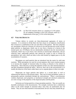
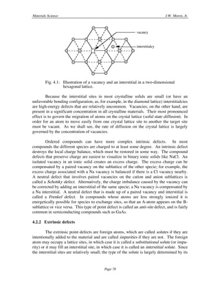
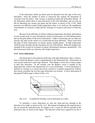
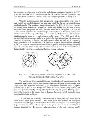
An edge dislocation in a simple cubic structure is drawn in Fig. 4.10, which
shows both a two-dimensional view and a three-dimensional section along the dislocation
line. The dislocation can be created by making a cut in the crystal on the dashed plane
that terminates at the dislocation line, displacing the material above the cut plane to the
left of the dislocation by one lattice spacing, and allowing the atoms to re-bond across the
slip plane. This recipe recreates the simple cubic unit cell everywhere except on the
dislocation line itself (ignoring the small elastic distortion of the cells that border the
dislocation line). Hence the Burgers vector, b, of the dislocation that is drawn in the
figure is b = a[100], where a is a vector along the edge of the cubic unit cell.
(a) (b)
Fig. 4.10: An edge dislocation in a simple cubic structure. The dotted
plane is the slip plane.
The process that creates the edge dislocation shown in Fig. 4.10 leaves one extra
vertical half-plane of atoms above the slip plane. This extra half-plane terminates at the
dislocation line, and is compressed there, as shown in the figure. The distortion at the
dislocation line is local. The simple cubic arrangement of atoms is essentially restored a
few atom spacings away from the dislocation line. The influence of the dislocation on
the atomic configuration rapidly decays into a small displacement that decreases in
magnitude with the inverse cube of the distance from the dislocation line. The local
distortion near the dislocation line (or dislocation core) is indicated in the figure.
In principle, the Burgers vector of a crystal dislocation can be any lattice vector;
for example, it is geometrically possible for an edge dislocation to be the termination of
any integral number of lattice planes. In reality, however, the Burgers vector is almost
invariably equal to the shortest lattice vector in the crystal. The reason is that the energy
per unit length of dislocation line, which is called the line energy, or, in a slightly
different context, the line tension of the dislocation, increases with the square of the
magnitude of b, |b|2. (While we shall not prove this, it is obvious from Fig. 4.10 that the
local distortion of the crystal would increase dramatically if two or more extra half-planes
terminated at the dislocation line.) Let the Burgers vector, b, be the vector sum of
13. Materials Science J.W. Morris, Jr.
Page 88
smaller lattice vectors, b = b1 + b2. Unless b1 and b2 are perpendicular, |(b1+b2)|2 >
|b1|2 + |b2|2, and the dislocation can decrease its energy by splitting into two or more
dislocations that have smaller Burgers vectors.
4.3.3 The Burgers circuit
While it is always possible to find the Burgers vector, b, of a dislocation by deter-
mining the slip that would be required to make it, this is often inconvenient. A simpler
method uses a geometric construction known as the Burgers circuit.
To construct the Burgers circuit, choose a direction for the dilocation line and
draw a clockwise closed circuit in the perfect crystal by taking unit steps along the lattice
vectors. An example is drawn for a {100} plane in a simple cubic crystal in Fig. 4.11. If
the same circuit is drawn so that it encloses a dislocation, it fails to close. The vector
(from the starting position) that is required to complete the circuit is the Burgers vector,
b, of the dislocation, and measures the net displacement experienced by an imaginary
observer who completes a circuit around the dislocation that would be closed in a perfect
crystal.
b
(a) (b)
Fig. 4.11: A Burgers circuit closes in a {100} plane of a cubic crystal,
but fails to close by the Burgers vector, b, when the same cir-
cuit encloses an edge dislocation.
4.3.4 Motion of an edge dislocation: glide and climb
The reason that dislocations control the plastic deformation of crystalline solids is
that it is relatively easy to move dislocations to produce shear deformation of the sort that
is pictured in Fig. 3.9. It would be enormously difficult to shear a crystal by forcing the
glide of rigid planes of atoms over one another; one would have to force the simultaneous
reconfiguration of every crystal bond that crossed the slip plane. The same result is more
easily achieved by moving dislocations stepwise through the crystal. Stepwise
dislocation motion requires a much smaller force since each elementary step can be
accomplished by reconfiguring only the bonds that neighbor the dislocation line.
14. Materials Science J.W. Morris, Jr.
Page 89
The stepwise motion of an edge dislocation in a simple cubic crystal is illustrated
in Fig. 4.12. In order for the dislocation to move one lattice spacing to the right it is only
necessary to break the bond indicated by the long dash in 4.12a and establish the bond in-
dicated by the short dash. The new configuration is shown in Fig. 4.12b. Of course one
bond must be broken for each plane through which the dislocation threads, so a
significant force is still required. But the force is small compared to that required to slip
the upper part of the crystal as a rigid body. If the dislocation moves through the crystal
in a sequence of individual steps like that shown in Fig. 4.12 it causes a net slip of the
material above its plane of motion by the Burgers vector, b, and hence causes a rigid
displacement of the whole upper part of the crystal.
(a) (b)
Fig. 4.12: Glide of an edge dislocation. Only a single bond must be
broken per plane for each increment of glide.
The type of motion that is illustrated in Fig. 4.12 is called dislocation glide, and is
relatively easy to accomplish. However, an edge dislocation cannot glide in an arbitrary
direction. It can only glide in a particular plane, the slip plane or glide plane, which con-
tains both the Burgers vector and the dislocation line.
(a) (b)
Fig. 4.13: Climb of an edge dislocation. Movement up out of the plane
requires the elimination of atoms by vacancies. Movement
down requires the addition of atoms.
When an edge dislocation moves out of its glide plane its motion is called climb.
The climb of a dislocation is difficult at ordinary temperatures since it requires that atoms
be absorbed on or liberated from the extra half-plane of atoms that defines the dislocation
line. The climb of an edge dislocation is illustrated in Fig. 4.13. The mechanism is
slightly different depending on whether the dislocation moves up, which contracts the
extra half-plane, or down, which extends it.
15. Materials Science J.W. Morris, Jr.
Page 90
If the dislocation climbs up atoms must be liberated from the edge of the extra
half-plane. Since the number of atoms is conserved, this requires the absorption of
vacancies from the lattice. One vacancy is needed per plane the dislocation threads. If
the dislocation climbs down it must add atoms to the extra half-plane, and can only do
this by liberating one vacancy per plane into the matrix, as shown in Fig. 4.13b. Both
processes are difficult except at high temperature when, as we shall see, the equilibrium
concentration of vacancies is high and the exchange of vacancies and atoms is relatively
easy.
Because of the difficulty of climb at ordinary temperatures the plastic deformation
of real crystals tends to occur through the motion of dislocations on well-defined planes
that are the glide planes of the active dislocations. Under a microscope one can often see
discrete slip steps on the surface of a crystal that has been deformed. These result from
the glide of many dislocations on closely spaced, parallel planes. At high temperature
climb becomes possible and the slip planes are less well-defined. When this happens the
strength of the crystal (its resistance to plastic deformation) decreases dramatically. For
this reason most solids are relatively soft at high temperature.
4.3.5 Screw dislocations
Our discussion to this point has dealt only with edge dislocations, that is, disloca-
tions in which the Burgers vector is perpendicular to the dislocation line. Dislocations in
real crystals rarely have a pure edge character. Their Burgers vectors lie at various angles
to their line directions. In the extreme case the Burgers vector is parallel to the
dislocation line, which is the characteristic of a screw dislocation. A screw dislocation is
difficult to visualize in a crystal, but can be created by a method suggested by Volterra
that closely resembles the way the edge dislocation was formed. A screw dislocation of
the general Volterra type is shown in Fig. 4.14.
“
b
Fig. 4.14: A method for forming a screw dislocation in a solid.
To introduce a screw dislocation we slice the solid part-way through in the
direction of its width, as shown in Fig. 4.14. But instead of displacing the material above
the cut toward the dislocation line we displace it by a vector, b, that lies parallel to the
dislocation line, as shown in the figure. The direction of the force required to do this is
16. Materials Science J.W. Morris, Jr.
Page 91
also indicated. The material is then re-welded so that it is continuous across the plane of
slip. The residual distortion is concentrated at the dislocation line, which then constitutes
an isolated linear defect.
If the body shown in Fig. 4.14 is crystalline then the cut surface shown in the fig-
ure is a plane of atoms. In order for the crystal to be continuous across the slip plane
after it is rejoined, the displacement, b, must be such that this plane of atoms joins
continuously onto a crystallographically identical plane. It follows that a closed circuit
(Burgers circuit) that encloses a screw dislocation not only fails to close, but produces a
net translation by b along the dislocation line, where b is a lattice vector. A circuit that
starts on one plane of atoms finishes on another a distance b below. Continuing the
circuit causes a displacement by b at each revolution, without the circuit ever leaving the
atom plane. The effect of a screw dislocation is to join a set of parallel atom planes so
that they become a single plane like one that would be created by extending a plane
outward from the thread of a screw. Hence the name: screw dislocation.
As in the case of an edge dislocation the line energy of a screw dislocation is pro-
portional to the square of its Burgers vector. Hence the Burgers vector of the screw
dislocation is ordinarily the smallest lattice vector that is compatible with the direction of
its line.
4.3.6 Screw dislocations and plastic deformation
A screw dislocation differs from an edge not only in its geometry but in the way it
accomplishes plastic deformation. The most important qualitative differences concern its
direction of motion under an applied force and its relative freedom of movement.
Figure 4.14 suggests the connection between slip and dislocation motion for a
screw dislocation. As the screw dislocation is displaced through the width of the body
the material above its plane is slipped in the direction of the Burgers vector, hence along
the length of the body. It follows that the longitudinal force shown in the figure acts to
drive the screw dislocation sideways. If a screw dislocation is passed through the full
width of the body it causes the shear shown in Fig. 3.8, which is the same as that caused
by the passage of an equivalent edge dislocation through the length.
In contrast to an edge dislocation, a screw dislocation can glide in any plane.
Since the Burgers vector lies parallel to the dislocation line both are in any plane that
contains the dislocation line, and the screw dislocation can move in any direction perpen-
dicular to its line.
4.3.7 Dislocations in real materials: mixed dislocations
Dislocations in real materials are most commonly neither pure edge nor pure
screw in their character, but are mixed dislocations whose Burgers vectors lie at an
intermediate angle to the local direction of the dislocation line. Because of the way in
which they interact with other elements of the microstructure (which we shall discuss at a
17. Materials Science J.W. Morris, Jr.
Page 92
later point) dislocation lines are ordinarily curved. Since the dislocation bounds a region
that has been slipped by the Burgers vector, b, the Burgers vector is the same at every
point on the dislocation line. Hence the character of a curved dislocation changes
continuously along its length. For this reason it is often most useful to think of a
dislocation as the boundary of a surface over which the crystal has slipped rather than as
a defect with a particular local atomic configuration.
b
screwedge
Fig. 4.15: A dislocation loop in a crystal.
This point is illustrated by the dislocation loop shown in Fig. 4.15. Dislocation
loops are relatively common features of the microstructures of structural alloys. The loop
shown in the figure is created by a process that is equivalent to a slip of the cylinder of
material above the loop by the vector b. The dislocation loop is the boundary of the
surface on which slip has occurred. The character of the dislocation changes
continuously around the loop. The dislocation has pure edge character at the extremities
of the loop along the length of the body, and has pure screw character at the extremities
along the width.
The qualitative nature of the force on a curved dislocation, such as the loop in Fig.
4.15, can also be understood by regarding it as the boundary of the slipped region. If the
force on the body is oriented to shear the body by the vector b then the dislocation will
tend to move so that it increases the area of slip; the loop will expand. If the force acts to
shear the body in the direction -b, the dislocation will tend to move so that it shrinks the
slipped area; the loop will contract.
Whether edge, screw or mixed in character, all dislocations have three important
properties. First, they bound surfaces that divide the crystal so that the part above the
surface is slipped by the vector, b, with respect to that below. Second, the slip on the
surface bounded by the dislocation is constant and equal to a lattice vector. Hence the
Burgers vector, b, is a lattice vector and has the same value at every point on the
dislocation line. Third, since the slip is constant, a dislocation cannot simply end within a
material; there is always a boundary between a slipped and an unslipped area. The
dislocation can terminate at a free surface, as in Fig. 4.7 and 4.14, it can close on itself, as
in Fig. 4.15, or it can end at a junction with other dislocations that bound surfaces over
which the magnitude or direction of slip is different.
18. Materials Science J.W. Morris, Jr.
Page 93
4.3.8 Partial dislocations
In the original concept of Volterra, the Burgers' vector of a crystal dislocation is a
translation vector of the crystal, that is, a vector that connects atom positions so that the
crystal can be rejoined perfectly across its glide plane. Such a dislocation is called a total
dislocation. The element of slip it induces carries an atom in the glide plane from one
atom position to another. Only total dislocations can be true two-dimensional defects. If
the Burgers' vector were not a translation vector of the crystal the slipped surfaces would
not weld perfectly together across the glide plane and a planar, surface defect would be
left behind whenever the dislocation moved.
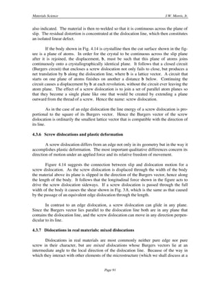
While most crystal dislocations are total dislocations when viewed from suffi-
ciently far away, it is not uncommon to find them dissociated locally into a configuration
that can be described as two parallel partial dislocations connected by a planar defect that
is called a stacking fault in the crystal. The prototypic example is found in FCC crystals.
B
C
A
A A
AA
A A
B
B
C C
bb1
b2
b
b1
b2
A
A
A
A
A
A
B
B
B
B
B
B
...
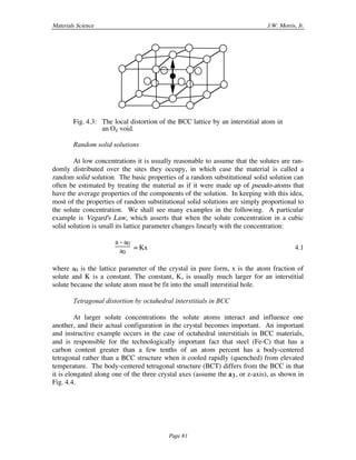
Fig. 4.16: Illustration of the slip of close-packed planes. The dashed ar-
row shows slip by a total dislocation, b = 1
2 [–101], which car-
ries B“B. The solid arrows show the competing process of
successive slip by two partial dislocations. The shaded atom
in the cell is the intermediate, C-site position reached after
partial slip.
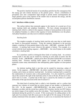
The common dislocation in the FCC structure is the dislocation that causes close-
packed planes to slip over one another. The close-packed planes are {111} planes, and
the Burgers' vectors of the dislocations that induce slip on these planes are the
1
2 <110>
vectors that connect atoms to their nearest neighbors in the {111} planes. Fig. 4.16 illus-
trates the path by which an FCC crystal is slipped by one atom spacing in the (111) plane.
The slip vector is
1
2 [–101], and is the slip caused by a dislocation with Burgers' vector b =
1
2 [–101]. Assuming that the glide plane of the dislocation lies between (111) planes of A
and B-type atom sites, the element of slip carries an atom from one B-site to another, as
shown in the figure. For clarity, the figure is drawn twice. The drawing on the left
shows the displacement in a stacking of close-packed planes (A,B). The drawing on the
right places the A and B planes in an FCC unit cell.
19. Materials Science J.W. Morris, Jr.
Page 94
Direct slip from one B position to another is relatively difficult, as one can easily
show by trying to slide two close-packed arrays of balls over one another. The atoms
(balls) in the B-plane must ride over the A atoms, as illustrated in the figure. It is much
easier to accomplish the slip in two sequential steps, as indicated in the figure, that cir-
cumvent the A atoms. The B atoms are first slipped into C positions, then moved from C
back to B again. The slip can be accomplished by the sequential passage of two disloca-
tions with the Burgers' vectors b1 and b2. However, b1 and b2 are not lattice vectors;
they are examples of partial dislocations. Their sum is the total dislocation, b.
B
B
BBB
B
A
CC
C
1/2[–1–12]
1/2[–211]
1/2[–101]
Fig. 4.17: Configuration of atoms in the (111) plane showing the partial
and total slip vectors.
To find the Burgers' vectors of the partial dislocations let the close-packed plane
be the (111) plane, as shown in the right-hand figure in 4.16. The atom shift is to the
shaded atom position, followed by a shift to the final atom position in the face center.
The (111) plane of B-sites in the unit cell in Fig. 4.16 is redrawn in Fig. 4.17. As shown
in this figure, the Burgers' vector of the total dislocation is b =
1
2 [–101]. The first partial
slip is from the B site at the corner of the unit cell to the nearest C-site in the plane. This
slip is 1/3 of the vector connecting B-sites along the height of the triangular configuration
of atoms in the plane, which is
1
2 [–1–12]. Hence
b1 =
1
6 [–1–12] 4.2
The second partial slip is from the C-site to the final B-site position. As shown in the fig-
ure, this vector is parallel to the vector
1
2 [–211}, and is 1/3 of its length. Hence
b2 =
1
6 [–211] 4.3
The vector sum of the two partial dislocation vectors is
b1 + b2 =
1
6 [–1–12] +
1
6 [–211] =
1
2 [–101] = b 4.4
20. Materials Science J.W. Morris, Jr.
Page 95
Splitting the total dislocation, b, into the partials, b1 and b2, not only facilitates
slip, but also lowers the total energy. The energy per unit length of dislocation line is
proportional to |b|2. Since
|b|2 > |b1|2 + |b2|2 4.5
the energy of a parallel pair of partial dislocations, b1 and b2, is less than that of the total
dislocation, b = b1 + b2.
“
b
b1b2
Fig. 4.18: The total dislocation, b, divided into partial dislocations, b1
and b2 separated by a stacking fault.
However, to understand the configuration that appears when the dislocation is
split we must recognize that eq. 4.5 gives only part of the energy of the pair of partials.
Let the total dislocation divide, as illustrated in Fig. 4.18. In the area between the
partials, which is shaded in the figure, the region above the slip plane has been slipped by
the vector b1, but has not yet experiences the slip b2. Let the slip plane lie between A
and B-planes, as illustrated in Fig. 4.16. The partial slip b1 carries the atoms in B-sites
into C-sites, and causes corresponding changes C“A and A“B in successively higher
planes. The FCC crystal has the stacking ..ABCABC.. But the stacking encountered in a
direction perpendicular to the glide plane that passes through the shaded area between the
partials is ..ABCA|CABC.., where the slash indicates the glide plane. The partial
dislocation perturbs the sequence of close-packed planes; it introduces a planar defect
called a stacking fault on the glide plane between the two partials.
A stacking fault has a positive energy, ßs, per unit area. The separation of the two
partials, b1 and b2, creates a stacking fault whose area increases as the partials move
apart. There is, therefore, an equilibrium separation between the partial dislocations.
They separate to decrease the energy per length of dislocation, but are attracted by the
need to minimize the stacking fault energy. The balance of these two effects determines
the equilibrium separation, which is of the order of 5-500‹ in typical FCC crystals.
Similar considerations apply to HCP and diamond cubic crystals. Total disloca-
tions in the close-packed planes tend to divide into partials separated by ribbons of
stacking fault. In BCC crystals the division of total dislocations into partials is much less
21. Materials Science J.W. Morris, Jr.
Page 96
pronounced. Separated partials cannot ordinarily be resolved in BCC, even through high
resolution electron microscopy. Their presence is inferred from features of the
mechanical behavior that are most easily explained by assuming that total dislocations
dissociate slightly.
4.4 TWO-DIMENSIONAL DEFECTS: INTERFACES
The two-dimensional defects that appear in crystals can be usefully divided into
three types: free surfaces, which are the external surfaces at which the solid terminates at
a vapor or liquid, intercrystalline boundaries, which separate grains or distinct phases
within the solid, and internal defects that disrupt the crystalline pattern over a surface
within a crystal. All of these defects have two important characteristics. First, since they
are surfaces in a crystal they have particular atomic structures that depend on orientation.
Second, they have a positive energy. The energy per unit area is ordinarily equal to the
surface tension, ß, of the interface.
4.4.1 Free surfaces
The interface between a crystalline solid and a vapor or liquid governs the interac-
tion between the two phases, and influences the behavior of the solid in many important
ways that we shall discuss later in the course. It also affects the shape of the solid. The
shape and properties of the free surface are determined by a combination of its structure
and its energy. These two parameters are related to one another.
solutes segregated
to interface
adsorbed molecule
adsorbed atom
...
Fig. 4.19: Solid surface showing segregated solutes and adsorbates.
The crystal structure of the solid extends up to the free surface. The structure of
the surface is derived from the pattern of atomic packing on the crystal plane that lies
parallel to the surface, and the behavior of the surface can often be inferred from that
pattern. However, the structure of the surface always differs at least a bit from that of a
crystal plane that parallels it within the bulk crystal. Even when the crystal sits in a
22. Materials Science J.W. Morris, Jr.
Page 97
perfect vacuum, the atoms in the free surface are bonded on only one side and the spacing
and the configuration of the atoms in the first few planes at the interface adjusts to
accommodate the asymmetry of the bonding in the bast possible way. The structure of a
real interface is further complicated by bonding interactions across the interface and by
chemical changes in the interfacial plane. The dangling bonds at the interface provide
favorable sites for the adsorption of atoms that do not fit well into the bulk lattice. The
interface is often enriched in solute species (surfactants). Oxygen, sulfur and
phosphorous are common surfactants in engineering solids.
(111)
(hkl)
...
Fig. 4.20: A surface of overall orientation (hkl) made up of close-
packed segments in steps.
The interfacial tension of the free surface depends on its structure, and is deter-
mined, in large part, by the number of bonds that are broken because the crystal is not
continued on the far side of the interface. As a consequence the interfacial tension, ß, is a
function of the orientation of the surface. In a typical metal, the interfacial tension is a
relatively weak function of the orientation. Because metallic bonding is relatively non-
directional, the interfacial tension of a typical metal tends to vary with the density of
packing in the interface and is minimized for surface orientations that parallel close-
packed planes ({111} in FCC, {110} in BCC). Covalent solids have fewer neighbors,
and more directional bonds, and are much more strongly anisotropic in their surface
tension.
The external surfaces of metallic and covalent solids tend to parallel the planes of
closest atomic packing, as illustrated in Fig. 4.19. This tendency also influences the
atomic structures of interfacial planes that have other orientations. An interface that does
not parallel a close-packed plane often has a structure in which flat, close-packed
segments form ledges of atomic height that give a stepped structure with the proper
overall orientation, as illustrated in Fig. 4.20. While the stepped morphology increases
the surface area, the overall surface tension is lower because of the relatively low surface
tension of the close-packed steps.
23. Materials Science J.W. Morris, Jr.
Page 98
= {111} plane
= {100} plane
Fig. 4.21: The NaCl structure, showing the electrical neutrality of the
{100} plane and the preferential charge on the {111} plane.
The interfacial tension of a surface in an ionic solid is strongly affected by the dis-
tribution of electric charge. In strongly ionic materials (for example, NaCl) the electri-
cally neutral surfaces ({100} in NaCl) have much lower interfacial tensions than the
charged surfaces (such as {111} (Fig. 4.21)). The relative interfacial tensions of charged
and uncharged surfaces can, of course, be altered by the addition of surfactants, which are
often preferentially attracted to the charged surfaces.
The shapes of crystals
The preferred shape of a crystal that is bounded by free surfaces is the one that
minimizes its total interfacial energy. The macroscopic surface of the crystal can always
be treated as if it were made up of facets, the kth one of which has area, Ak , and
interfacial tension, ßk. The energy is, then,
E = ∑
k
ßkAk 4.5
When the crystal is a simple metal the surface tension is nearly isotropic. The preferred
shape is nearly spherical, since a spherical shape minimizes the surface area for given
volume. When the crystal is ionic or strongly covalent there are crystal planes whose
tensions are, relatively, very low. To minimize the total interfacial energy, ionic and
covalent solids tend to assume polygonal shapes with large, flat facets parallel to the low-
energy planes.
This is the physical reason that compound solids and minerals often look crys-
talline, while metals usually do not. The natural macroscopic shapes of such compounds
are polygonal (crystalline) because of the strong anisotropy of the surface tension. You
can readily verify, for example, that the grains of common table salt have a cubic shape;
this shape reflects the low energy of the neutral {100} surfaces in the NaCl structure.
Many common minerals have hexagonal structures in which the prismatic planes (the
vertical planes in the hexagonal unit cell) are electrically neutral. These materials tend to
grow as well-shaped hexagonal prisms. Simple metals, on the other hand, are more
24. Materials Science J.W. Morris, Jr.
Page 99
isotropic in their interfacial tensions, and tend to form crystals that are cylindrical or
spherical in their macroscopic shapes.
The shapes of crystals can be altered and controlled by adding selective chemical
surfactants that modify the surface tensions of particular planes. For example, NaCl can
be made to crystallize in an irregular particle with mainly {111} faces by adding a
suitable surfactant.
Solid-liquid interfaces
The interface between a crystalline solid and a vapor is usually sharp. The
surface is a crystal plane or stepped layer of planes. Interfaces between solids and
liquids, on the other hand, are often diffuse. There is a high density of atoms in the liquid
near the solid surface, and these may have a local arrangement that does not differ that
greatly from the crystalline pattern in the solid. In these cases the tension of the solid-
liquid interface is a weak function of surface orientation, and the solid adopts a diffuse
interfacial structure like that shown in Fig. 4.22.
Fig. 4.22: Possible configuration of a diffuse interface.
The possibility of forming a diffuse interface is important in the solidification of
solids from the melt and the growth of crystals from the melt. Atoms of the liquid can be
easily incorporated into a diffuse interface, with the consequence that a solid that has
such an interface can solidify easily and rapidly.
4.4.2 Interfaces between crystals
The most important internal interfaces in a typical solid are those that separate the
individual crystallites it contains. Almost all crystalline solids are polycrystalline. They
are composed of many small crystallites (grains) of the primary constituent, and may also
contain several distinct constituents (phases) of different composition and crystal
structure. The interfaces that separate grains are called grain boundaries. Those that
separate phases are called two-phase interfaces.
Grain boundaries
25. Materials Science J.W. Morris, Jr.
Page 100
The structure of a grain boundary depends on the misorientation of the crystal
grains that it separates. When the misorientation is small the boundary, which is then
called a low-angle boundary, is a reasonably simple planar array of dislocations. When
the misorientation is larger the boundary structure is more complicated, and it is often
useful to picture the boundary as simply a region of disorder between the two crystal
grains.
= second phase
= primary grains
...
Fig. 4.23: Schematic drawing of polygranular grain structure showing
grain boundaries and two-phase interfaces.
The structure of a low-angle tilt boundary is shown in Fig. 4.24. A tilt boundary
is a vertical array of parallel edge dislocations. When a tilt boundary is introduced into a
single crystal it creates a misorientation by the tilt angle, œ, between the volumes of
crystal on either side. If the dislocations in the boundary have Burgers' vector, b, and are
separated by a vertical distance, d, then the tilt angle, œ, is given by
œ = tan-1
|b|
d 4.7
...
Fig. 4.24: A low-angle tilt boundary as a vertical array of parallel edge
dislocations.
A second type of low-angle boundary that can also be generated by a simple array
of dislocations is a twist boundary. If two sets of parallel screw dislocations are arrayed
in a perpendicular pattern in a plane the result is a twist in the boundary plane. The
crystal on one side of the plane is rotated with respect to that on the other by a twist angle
about an axis perpendicular to the plane of the boundary. A twist boundary is not simple
to draw, and we shall not attempt to do so here.
26. Materials Science J.W. Morris, Jr.
Page 101
The structures of high-angle grain boundaries can be crudely understood by
simply matching two crystals that are misoriented by the angle of the boundary. As
illustrated in Fig. 4.25, this process ordinarily leads to a relatively poor match of crystal
planes along the boundary. While there are relaxations in the boundary that reduce its
disorder somewhat, a typical high-angle boundary is relatively disordered, with a high
density empty spaces and open channels. High-angle grain boundaries provide easy
paths for atom diffusion in the solid state. They also provide preferential sites for solutes
and impurities that do not fit very well in the bulk crystal, and adsorb as surfactants on
the boundary.
Fig. 4.25: A possible configuration of a high-angle grain boundary.
There are, however, certain high-angle boundaries whose misorientations provide
a relatively good geometric match between the adjacent crystals. These are called
coincidence boundaries. Their study is beyond the scope of this course.
The equilibrium shape of a grain
...
Fig. 4.26: Ideal hexagonal configuration of a two-dimensional grain
structure with constant ßB.
The interfacial tension of a grain boundary is often a relatively weak function of
its orientation; for most purposes we can assume that it has the constant value, ßB. When
this is true a local equilibrium is achieved when grain boundaries meet in three-grain
27. Materials Science J.W. Morris, Jr.
Page 102
junctions in a configuration in which the angle between adjacent boundaries is 120º.
When the grain structure is two-dimensional, as it is in a thin film one grain thick, then
local equilibrium is achieved when the grains are hexagonal platelets, as in Fig. 4.26.
When the grain structure is three-dimensional a microstructure that is very near to
local equilibrium can be built up of fourteen-sided polyhedra that are known as Thomson
tetrakaidecahedra. The tetrakaidecahedron is shown in Fig. 4.27. It looks very complex
but, in fact, has a very simple construction. If one takes a body centered cubic array of
points and constructs planes that bisect the lines connecting a given point to its first and
second nearest neighbors, the inner envelope of these planes is the tetrakaidecahedron.
The tetrakaidecahedron is just the Wigner-Seitz cell of the BCC structure. It follows that
tetrakaidecahedra stack in a body-centered cubic array. The BCC array of te-
trakaidecahedra is sometimes useful as a model of a three-dimensional microstructure.
However, its accuracy is limited; real polygranular solids are built up of irregularly
shaped grains that have a distribution of sizes and an irregular pattern in space (as in Fig.
4.22). The grains in real microstructures are never quite in minimum-energy configura-
tions. A somewhat better model of a real microstructure is a three-dimensional foam of
the type that forms on beverages that are familiar to undergraduates.
(a) (b)
Fig. 4.27: (a) Thomson tetrakaidecahedron inscribed in a cube. (b)
Packing of tetrakaidecahedra into a BCC array.
The positive surface tension of the grain boundary has the consequence that the
energy of a polygranular material increases in proportion to the total grain boundary area.
Large grains have a smaller surface energy per unit volume than small ones. If a poly-
granular solid is held at high temperature where the atoms are relatively mobile then
grains can grow or shrink by adding or losing atoms to adjacent grains. The large grains
grow at the expense of the smaller ones to decrease the energy, which causes the mean
grain size to increase with time.
The grain structure is usually characterized by its mean grain size, which is mea-
sured as the mean grain diameter. The mean grain size provides an incomplete
characterization of the grain structure; both the distribution of grain sizes and the grain
shape are also important. These aspects of the grain structure are more difficult to
measure quantitatively. In practice a characterization of the grain structure usually
28. Materials Science J.W. Morris, Jr.
Page 103
consists of a value for the mean grain size and a set of photomicrographs that present the
geometrical features of the grain structure in visual form.
Two-phase interfaces
Two-phase interfaces have many of the properties of grain boundaries, including a
specific structure and interfacial energy. The most important structural characteristic of a
two-phase interface is its coherency. If it is possible to order the phases on both sides of
the interface on the same crystal lattice the interface is said to be coherent. A two-dimen-
sional example is given in Fig. 4.28. Coherent interfaces are common in real systems.
When small precipitates form in the interior of a solid the precipitate phase that forms
first usually involves only a slightly different atomic ordering on the lattice of the parent
structure and has a coherent interface with it. In the modern science of thin-film
electronics multi-layer structures are often deposited atom layer by atom layer from the
vapor phase, to create a heterostructure of atom layers of different composition that are
coherent with one another.
Fig. 4.28: Coherent, ordered precipitate in a two-dimensional crystal.
On the other hand, since two different crystalline phases almost never fit perfectly
together, both are distorted if they are joined by a coherent interface. In the case of a
small precipitate particle the lattice distortion that is caused by the coherent interface in-
creases with the particle size, and provides an increasing driving force to destroy
continuity at the interface. When a second-phase particle grows to large size it almost
always loses coherency with the surrounding matrix. The most common mechanism
causing the loss of coherency is the accumulation of dislocations at the interface.
The surface tension of a coherent two-phase interface is highly anisotropic since
the two phases only fit well when they have a simple crystallographic relation to one
another. The volumetric distortion of the precipitate also depends strongly on its shape
and crystallographic fit. As a consequence, coherent second-phase particles such as small
precipitates tend to have characteristic shapes and interfaces that lie almost entirely in a
particular crystallographic plane of the parent crystal, which is known as the habit plane
of the precipitate. The well-defined habit is lost when the precipitate is incoherent.
29. Materials Science J.W. Morris, Jr.
Page 104
The positive interfacial tension of second-phase particles has the consequence that
the energy per unit volume decreases as the particle grows. Given a distribution of
precipitate sizes and a temperature high enough to permit atomic rearrangements the
larger particles grow at the expense of the smaller ones to decrease the energy, and the
second-phase particle distribution coarsens.
4.4.3 Interfaces within crystals
The surface defects that commonly appear in the interior of a crystal are of two
types: stacking faults and antiphase boundaries. We have already encountered the
stacking fault, which is a defect in the sequence of planes of atom positions in the crystal.
An antiphase boundary is a defect in the sequence of atom distributions over the planes.
Anti-phase boundaries can only occur in ordered compounds.
Stacking faults
The simplest examples of stacking faults (and the only ones that we shall study)
are found in close-packed structures. Using the notation introduced in the previous
chapter, a stacking of close-packed planes in the order ...ABCABC... generates the FCC
structure. A stacking fault occurs wherever this pattern is broken. For example, in a
crystal with the local stacking sequence ...ABCBABC... the extra B plane in the middle
constitutes a stacking fault.
It is sometimes useful to distinguish three kinds of stacking fault. An extrinsic
stacking fault is one that can be created by inserting an extra plane of atoms into the
structure. In the ...ABC|B|ABC... pattern given above the plane marked |B| is an extrinsic
stacking fault. Extrinsic stacking faults appear, for example, after an irradiation
treatment creates many interstitialcies that subsequently gather together on close-packed
planes.
An intrinsic stacking fault is one that can be created by removing a plane of
atoms. In the sequence ...ABC||BCABC.. the defect marked || corresponds to a missing
A-plane, and is hence an intrinsic stacking fault. An intrinsic stacking fault is created by
the condensation of vacancies onto a close-packed plane. It is also created by a partial
slip of the crystal to the right of the fault that carries A-sites to B-sites, B-sites to C-sites,
and C-sites to A-sites. A partial slip of this type is caused by the motion of a partial
dislocation of the type discussed at the end of section 4.3.
The third kind of stacking fault is called a twin boundary, and is a surface that
separates two volumes of crystal that are mirror images of one another, as illustrated in
Fig. 4.28. In the sequence ...ABCAB|C|BACBA... the plane marked C is a twin
boundary; on either side the crystal has a perfect FCC structure, but the two FCC lattices
are mirror images of one another across the twin plane. Twin boundaries are most often
introduced during the growth of a crystal. If the crystal grows by adding planes to the
right and if an extrinsic fault (B) occurs just to the right of |C|, the energy of the fault is
usually minimized if the next plane is added at A, and so on, to maximize the fraction of
30. Materials Science J.W. Morris, Jr.
Page 105
proper FCC packing in the crystal. The formation of twin boundaries is also important in
the plastic deformation of some materials, as we shall discuss later in the course.
...
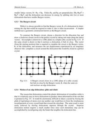
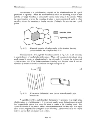
Fig. 4.29: The relation of crystal planes across a twin boundary.
Note that if a stacking fault is repeated with perfect periodicity it does not
constitute a fault, but creates a new crystal structure. For example, the sequences
ABCAB, ABCABCAB, and ABABABC are regular mixtures of FCC and HCP packing
that generate new structures if they are repeated indefinitely. Such mixed structures
occur in nature. They are usually found in materials that exhibit both FCC and HCP-type
structures, which indicates that the stacking fault energy is relatively small. Mixed
structures are particularly common in SiC, ZnS and CdS, all of which have alternate å-
ZnS (FCC) and ∫-ZnS (HCP) structures. The mixed structures are called polytypes, and
can have very long repeat periods.
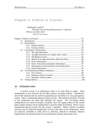
Antiphase boundaries
The internal defects known as antiphase boundaries only occur in ordered com-
pounds. An example is given in Fig. 4.30, which illustrates a {110} antiphase boundary
in a compound with the CsCl structure.
An ordered compound can always be regarded as a stacking of parallel planes,
each of which has a particular substitutional pattern of the atomic species. Fig. 4.30a, for
example, illustrates how the CsCl structure can be made by stacking {110} planes that
alternate in the specific arrangement of the two types of atoms. An antiphase boundary is
created when a plane with the wrong pattern appears, and subsequent planes follow it in
their patterns. In Fig. 4.29b the third {110} plane has its atom positions shifted by
1
2
<110> from the expected pattern, and is, hence, an antiphase defect. An antiphase
boundary resembles an intrinsic stacking fault in that it can be created either by omitting
one plane in the stacking pattern, or by a slip displacement at the antiphase plane.
Mechanical slip is an important source of antiphase defects. Note that the antiphase
defect in Fig. 4.30b is precisely that which would be created if a dislocation of Burgers
vector
1
2 [110] passed through the plane. Since
1
2 [110] is a vector connecting nearest
neighbor atoms in the closest-packed planes of the BCC structure, it is a common
Burgers vector for dislocations in BCC.
31. Materials Science J.W. Morris, Jr.
Page 106
(a) (b)
Fig. 4.30: (a) The CsCl structure drawn as a stacking of {110} planes.
(b) An antiphase boundary in the CsCl structure made by a
displacement of the type
1
2 <110> in the third plane.
4.5 VOLUME DEFECTS
Volume defects in crystals are three-dimensional aggregates of atoms or
vacancies. It is common to divide them into four classes in an imprecise classification
that is based on a combination of the size and effect of the particle. The four categories
are: precipitates, which are a fraction of a micron in size and decorate the crystal; second-
phase particles or dispersants, which vary in size from a fraction of a micron to the
normal grain size (10-100µm), but are intentionally introduced into the microstructure;
inclusions, which vary in size from a few microns to macroscopic dimensions, and are
relatively large, undesirable particles that entered the system as dirt or formed by
precipitation; and voids, which are holes in the solid formed by trapped gases or by the
accumulation of vacancies.
Precipitates are small particles that are introduced into the matrix by solid state
reactions. While precipitates are used for several purposes, their most common purpose
is to increase the strength of structural alloys by acting as obstacles to the motion of
dislocations. Their efficiency in doing this depends on their size, their internal properties,
and their distribution through the lattice. However, their role in the microstructure is to
modify the behavior of the matrix rather than to act as separate phases in their own right.
Dispersants are larger particles that behave as a second phase as well as
influencing the behavior of the primary phase. They may be large precipitates, grains, or
polygranular particles distributed through the microstructure. When a microstructure
contains dispersants such properties as mechanical strength and electrical conductivity
are some average of the properties of the dispersant phase and the parent.
Inclusions are foreign particles or large precipitate particles. They are usually un-
desirable constituents in the microstructure. For example, inclusions have a deleterious
effect on the useful strength of structural alloys since they are preferential sites for
failure. They are also often harmful in microelectronic devices since they disturb the ge-
32. Materials Science J.W. Morris, Jr.
Page 107
ometry of the device by interfering in manufacturing, or alter its electrical properties by
introducing undesirable properties of their own.
Voids (or pores) are caused by gases that are trapped during solidification or by
vacancy condensation in the solid state. They are almost always undesirable defects.
Their principal effect is to decrease mechanical strength and promote fracture at small
loads.