Pardeep et al Int. Journal of Engineering Research and Applications www.ijera.com
ISSN : 2248-9622, Vol. 4, Issue 3( Version 1), March 2014, pp.569-573
www.ijera.com 569 | P a g e
Clocked Regenerative Comparators
Pardeep*, Abhishek Agal*, Bal Krishan**
* (Electronics Engineering Department, YMCA University of Science & Technology, Faridabad)
** (A.P., Electronics Engineering Department, YMCA University of Science & Technology, Faridabad)
ABSTRACT
Analog to Digital Conversion is a process in which analog signal is changed into digital signal without changing
its contents. A low power, low delay and a high speed analog to digital convertor uses clocked regenerative
comparators for the reduction in Delay and Power. In this paper Transient analysis on the delay of clocked
regenerative comparators is presented. Technology used for the simulation process is 180nm which shows
reduced delay time up to 30% in Conventional Double-Tail Comparator i.e. 2.9088e-009 sec. at 0.8V.
Keywords - Clocked regenerative comparator, Conventional comparators, DTC.
I. INTRODUCTION
Comparator is a circuit that compares an
analog signal (voltage) with another analog voltage
or reference voltage and outputs a binary signal based
on the comparison.
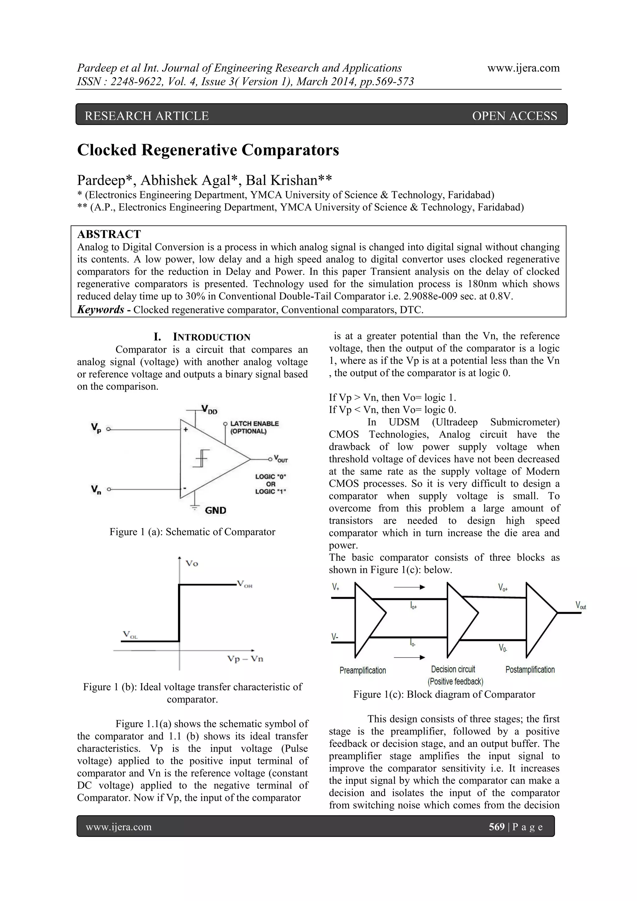
Figure 1 (a): Schematic of Comparator
Figure 1 (b): Ideal voltage transfer characteristic of
comparator.
Figure 1.1(a) shows the schematic symbol of
the comparator and 1.1 (b) shows its ideal transfer
characteristics. Vp is the input voltage (Pulse
voltage) applied to the positive input terminal of
comparator and Vn is the reference voltage (constant
DC voltage) applied to the negative terminal of
Comparator. Now if Vp, the input of the comparator
is at a greater potential than the Vn, the reference
voltage, then the output of the comparator is a logic
1, where as if the Vp is at a potential less than the Vn
, the output of the comparator is at logic 0.
If Vp > Vn, then Vo= logic 1.
If Vp < Vn, then Vo= logic 0.
In UDSM (Ultradeep Submicrometer)
CMOS Technologies, Analog circuit have the
drawback of low power supply voltage when
threshold voltage of devices have not been decreased
at the same rate as the supply voltage of Modern
CMOS processes. So it is very difficult to design a
comparator when supply voltage is small. To
overcome from this problem a large amount of
transistors are needed to design high speed
comparator which in turn increase the die area and
power.
The basic comparator consists of three blocks as
shown in Figure 1(c): below.
Figure 1(c): Block diagram of Comparator
This design consists of three stages; the first
stage is the preamplifier, followed by a positive
feedback or decision stage, and an output buffer. The
preamplifier stage amplifies the input signal to
improve the comparator sensitivity i.e. It increases
the input signal by which the comparator can make a
decision and isolates the input of the comparator
from switching noise which comes from the decision
RESEARCH ARTICLE OPEN ACCESS
Pardeep et al Int. Journal of Engineering Research and Applications www.ijera.com
ISSN : 2248-9622, Vol. 4, Issue 3( Version 1), March 2014, pp.569-573
www.ijera.com 570 | P a g e
stage. This is used to determine which of the input
signals is large. The output buffer amplifies this
information and gives a digital output signal.
II. CLOCKED REGENERATIVE
COMPARATORS
Clocked regenerative comparators have
found wide applications in many high-speed ADCs
since they can make fast decisions due to the strong
positive feedback in the regenerative latch.
Conventional Dynamic Comparator and Double tail
conventional dynamic comparator are discussed
below.
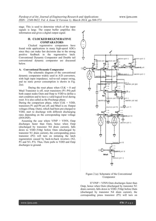
A. Conventional Dynamic Comparator
The schematic diagram of the conventional
dynamic comparator widely used in A/D converters,
with high input impedance, rail-to-rail output swing,
and no static power consumption is shown in Fig.
2(a).
During the reset phase when CLK = 0 and
Mtail Transistor is off, reset transistors (P1–P4) pull
both output nodes Outn and Outp to VDD to define a
start condition and to have a valid logical level during
reset. It is also called as the Precharge phase.
During the comparison phase, when CLK = VDD,
transistors P1 and P4 are off, and Mtail is on. Output
voltages (Outp, Outn), which had been pre-charged to
VDD, start to discharge with different discharging
rates depending on the corresponding input voltage
(INN/INP).
Assuming the case where VINP > VINN, Outp
discharges faster than Outn, hence when Outp
(discharged by transistor N4 drain current), falls
down to VDD–|Vthp| before Outn (discharged by
transistor N1 drain current), the corresponding pmos
transistor (P2) will turn on initiating the latch
regeneration caused by back-to-back inverters (N2,
P2 and N3, P3). Thus, Outn pulls to VDD and Outp
discharges to ground.
Figure 2 (a): Schematic of the Conventional
Comparator
If VINP < VINN Outn discharges faster than
Outp, hence when Outn (discharged by transistor N1
drain current), falls down to VDD–|Vthp| before Outn
(discharged by transistor N4 drain current), the
corresponding pmos transistor (P3) will turn on
P1 P2 P3 P4
N1
N2 N3
N4
Mtail
Pardeep et al Int. Journal of Engineering Research and Applications www.ijera.com
ISSN : 2248-9622, Vol. 4, Issue 3( Version 1), March 2014, pp.569-573
www.ijera.com 571 | P a g e
initiating the latch regeneration caused by back-to-
back inverters (N3, P3 and N2, P2). Thus, Outp pulls
to VDD and Outn discharges to ground.
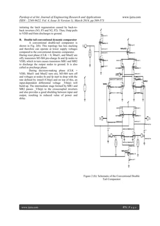
B. Double tail conventional dynamic comparator
A conventional double-tail comparator is
shown in Fig. 2(b). This topology has less stacking
and therefore can operate at lower supply voltages
compared to the conventional dynamic comparator.
During reset phase (CLK = 0, Mtail1, and Mtail2 are
off), transistors M3-M4 pre-charge fn and fp nodes to
VDD, which in turn causes transistors MR1 and MR2
to discharge the output nodes to ground. It is also
called as precharge phase.
During decision-making phase (CLK =
VDD, Mtail1 and Mtail2 turn on), M3-M4 turn off
and voltages at nodes fn and fp start to drop with the
rate defined by imtail1/Cfn(p) and on top of this, an
input-dependent differential voltage _Vfn(p) will
build up. The intermediate stage formed by MR1 and
MR2 passes _Vfn(p) to the crosscoupled inverters
and also provides a good shielding between input and
output, resulting in reduced value of power and
delay.
Figure 2 (b): Schematic of the Conventional Double
Tail Comparator
MR1
MR2
Mtail2
Mtail1
Pardeep et al Int. Journal of Engineering Research and Applications www.ijera.com
ISSN : 2248-9622, Vol. 4, Issue 3( Version 1), March 2014, pp.569-573
www.ijera.com 572 | P a g e
III. Result and analysis
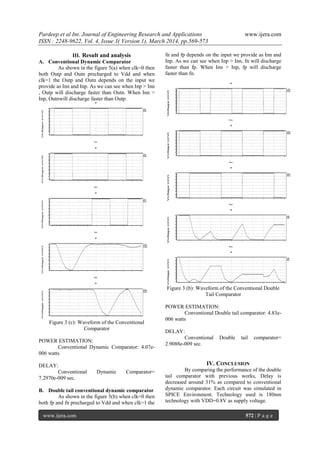
A. Conventional Dynamic Comparator
As shown in the figure 5(a) when clk=0 then
both Outp and Outn precharged to Vdd and when
clk=1 the Outp and Outn depends on the input we
provide as Inn and Inp. As we can see when Inp > Inn
, Outp will discharge faster than Outn. When Inn >
Inp, Outnwill discharge faster than Outp.
Figure 3 (c): Waveform of the Conventional
Comparator
POWER ESTIMATION:
Conventional Dynamic Comparator: 4.07e-
006 watts
DELAY:
Conventional Dynamic Comparator=
7.2970e-009 sec.
B. Double tail conventional dynamic comparator
As shown in the figure 5(b) when clk=0 then
both fp and fn precharged to Vdd and when clk=1 the
fn and fp depends on the input we provide as Inn and
Inp. As we can see when Inp > Inn, fn will discharge
faster than fp. When Inn > Inp, fp will discharge
faster than fn.
Figure 3 (b): Waveform of the Conventional Double
Tail Comparator
POWER ESTIMATION:
Conventional Double tail comparator: 4.83e-
006 watts
DELAY:
Conventional Double tail comparator=
2.9088e-009 sec.
IV. CONCLUSION
By comparing the performance of the double
tail comparator with previous works, Delay is
decreased around 31% as compared to conventional
dynamic comparator. Each circuit was simulated in
SPICE Environment. Technology used is 180nm
technology with VDD=0.8V as supply voltage.
Pardeep et al Int. Journal of Engineering Research and Applications www.ijera.com
ISSN : 2248-9622, Vol. 4, Issue 3( Version 1), March 2014, pp.569-573
www.ijera.com 573 | P a g e
REFERENCES
[1] Analysis and Design of a Low-Voltage
Low-Power Double-Tail Comparator by
Samaneh Babayan-Mashhadi, Student
Member, IEEE, and Reza Lotfi, Member,
IEEE Sept. 2013
[2] Design and Simulation of a High Speed
CMOS Comparator Smriti Shubhanand*,
Dr. H.P. Shukla, and A.G. Rao
[3] High Speed CMOS Comparator Design with
5mv Resolution by Raghava Garipelly
[4] A. Mesgarani, M. N. Alam, F. Z. Nelson,
and S. U. Ay, “Supply boosting technique
for designing very low-voltage mixed-signal
circuits in standard CMOS,” in Proc. IEEE
Int. Midwest Symp. Circuits Syst. Dig.
Tech. Papers, Aug. 2010, pp. 893–896.
[5] B. J. Blalock, “Body-driving as a Low-
Voltage Analog Design Technique for
CMOS technology,” in Proc. IEEE
Southwest Symp. Mixed-Signal Design,
Feb. 2000, pp. 113–118.
[6] M. Maymandi-Nejad and M. Sachdev, “1-bit
quantiser with rail to rail input range for
sub-1V __ modulators,” IEEE Electron.
Lett., vol. 39, no. 12, pp. 894–895, Jan.
2003.
[7] Y. Okaniwa, H. Tamura, M. Kibune, D.
Yamazaki, T.-S. Cheung, J. Ogawa, N.
Tzartzanis, W. W. Walker, and T. Kuroda,
“A 40Gb/ s CMOS clocked comparator with
bandwidth modulation technique,” IEEE J.
Solid-State Circuits, vol. 40, no. 8, pp.
1680–1687, Aug. 2005
[8] B. Goll and H. Zimmermann, “A
comparator with reduced delay time in 65-
nm CMOS for supply voltages down to
0.65,” IEEE Trans. Circuits Syst. II, Exp.
Briefs, vol. 56, no. 11, pp. 810–814, Nov.
2009.
[9] S. U. Ay, “A sub-1 volt 10-bit supply
boosted SAR ADC design in standard
CMOS,” Int. J. Analog Integr. Circuits
Signal Process. vol. 66, no. 2, pp. 213–221,
Feb. 2011.
[10] Allen, P.E and Holberg, D.R CMOS Analog
Circuit Design, Second Edition, New York,
Oxford University Press Inc., 2002, ISBN 0-
19-511644-5.

Cw4301569573

  • 1.
    Pardeep et alInt. Journal of Engineering Research and Applications www.ijera.com ISSN : 2248-9622, Vol. 4, Issue 3( Version 1), March 2014, pp.569-573 www.ijera.com 569 | P a g e Clocked Regenerative Comparators Pardeep*, Abhishek Agal*, Bal Krishan** * (Electronics Engineering Department, YMCA University of Science & Technology, Faridabad) ** (A.P., Electronics Engineering Department, YMCA University of Science & Technology, Faridabad) ABSTRACT Analog to Digital Conversion is a process in which analog signal is changed into digital signal without changing its contents. A low power, low delay and a high speed analog to digital convertor uses clocked regenerative comparators for the reduction in Delay and Power. In this paper Transient analysis on the delay of clocked regenerative comparators is presented. Technology used for the simulation process is 180nm which shows reduced delay time up to 30% in Conventional Double-Tail Comparator i.e. 2.9088e-009 sec. at 0.8V. Keywords - Clocked regenerative comparator, Conventional comparators, DTC. I. INTRODUCTION Comparator is a circuit that compares an analog signal (voltage) with another analog voltage or reference voltage and outputs a binary signal based on the comparison. Figure 1 (a): Schematic of Comparator Figure 1 (b): Ideal voltage transfer characteristic of comparator. Figure 1.1(a) shows the schematic symbol of the comparator and 1.1 (b) shows its ideal transfer characteristics. Vp is the input voltage (Pulse voltage) applied to the positive input terminal of comparator and Vn is the reference voltage (constant DC voltage) applied to the negative terminal of Comparator. Now if Vp, the input of the comparator is at a greater potential than the Vn, the reference voltage, then the output of the comparator is a logic 1, where as if the Vp is at a potential less than the Vn , the output of the comparator is at logic 0. If Vp > Vn, then Vo= logic 1. If Vp < Vn, then Vo= logic 0. In UDSM (Ultradeep Submicrometer) CMOS Technologies, Analog circuit have the drawback of low power supply voltage when threshold voltage of devices have not been decreased at the same rate as the supply voltage of Modern CMOS processes. So it is very difficult to design a comparator when supply voltage is small. To overcome from this problem a large amount of transistors are needed to design high speed comparator which in turn increase the die area and power. The basic comparator consists of three blocks as shown in Figure 1(c): below. Figure 1(c): Block diagram of Comparator This design consists of three stages; the first stage is the preamplifier, followed by a positive feedback or decision stage, and an output buffer. The preamplifier stage amplifies the input signal to improve the comparator sensitivity i.e. It increases the input signal by which the comparator can make a decision and isolates the input of the comparator from switching noise which comes from the decision RESEARCH ARTICLE OPEN ACCESS
  • 2.
    Pardeep et alInt. Journal of Engineering Research and Applications www.ijera.com ISSN : 2248-9622, Vol. 4, Issue 3( Version 1), March 2014, pp.569-573 www.ijera.com 570 | P a g e stage. This is used to determine which of the input signals is large. The output buffer amplifies this information and gives a digital output signal. II. CLOCKED REGENERATIVE COMPARATORS Clocked regenerative comparators have found wide applications in many high-speed ADCs since they can make fast decisions due to the strong positive feedback in the regenerative latch. Conventional Dynamic Comparator and Double tail conventional dynamic comparator are discussed below. A. Conventional Dynamic Comparator The schematic diagram of the conventional dynamic comparator widely used in A/D converters, with high input impedance, rail-to-rail output swing, and no static power consumption is shown in Fig. 2(a). During the reset phase when CLK = 0 and Mtail Transistor is off, reset transistors (P1–P4) pull both output nodes Outn and Outp to VDD to define a start condition and to have a valid logical level during reset. It is also called as the Precharge phase. During the comparison phase, when CLK = VDD, transistors P1 and P4 are off, and Mtail is on. Output voltages (Outp, Outn), which had been pre-charged to VDD, start to discharge with different discharging rates depending on the corresponding input voltage (INN/INP). Assuming the case where VINP > VINN, Outp discharges faster than Outn, hence when Outp (discharged by transistor N4 drain current), falls down to VDD–|Vthp| before Outn (discharged by transistor N1 drain current), the corresponding pmos transistor (P2) will turn on initiating the latch regeneration caused by back-to-back inverters (N2, P2 and N3, P3). Thus, Outn pulls to VDD and Outp discharges to ground. Figure 2 (a): Schematic of the Conventional Comparator If VINP < VINN Outn discharges faster than Outp, hence when Outn (discharged by transistor N1 drain current), falls down to VDD–|Vthp| before Outn (discharged by transistor N4 drain current), the corresponding pmos transistor (P3) will turn on P1 P2 P3 P4 N1 N2 N3 N4 Mtail
  • 3.
    Pardeep et alInt. Journal of Engineering Research and Applications www.ijera.com ISSN : 2248-9622, Vol. 4, Issue 3( Version 1), March 2014, pp.569-573 www.ijera.com 571 | P a g e initiating the latch regeneration caused by back-to- back inverters (N3, P3 and N2, P2). Thus, Outp pulls to VDD and Outn discharges to ground. B. Double tail conventional dynamic comparator A conventional double-tail comparator is shown in Fig. 2(b). This topology has less stacking and therefore can operate at lower supply voltages compared to the conventional dynamic comparator. During reset phase (CLK = 0, Mtail1, and Mtail2 are off), transistors M3-M4 pre-charge fn and fp nodes to VDD, which in turn causes transistors MR1 and MR2 to discharge the output nodes to ground. It is also called as precharge phase. During decision-making phase (CLK = VDD, Mtail1 and Mtail2 turn on), M3-M4 turn off and voltages at nodes fn and fp start to drop with the rate defined by imtail1/Cfn(p) and on top of this, an input-dependent differential voltage _Vfn(p) will build up. The intermediate stage formed by MR1 and MR2 passes _Vfn(p) to the crosscoupled inverters and also provides a good shielding between input and output, resulting in reduced value of power and delay. Figure 2 (b): Schematic of the Conventional Double Tail Comparator MR1 MR2 Mtail2 Mtail1
  • 4.
    Pardeep et alInt. Journal of Engineering Research and Applications www.ijera.com ISSN : 2248-9622, Vol. 4, Issue 3( Version 1), March 2014, pp.569-573 www.ijera.com 572 | P a g e III. Result and analysis A. Conventional Dynamic Comparator As shown in the figure 5(a) when clk=0 then both Outp and Outn precharged to Vdd and when clk=1 the Outp and Outn depends on the input we provide as Inn and Inp. As we can see when Inp > Inn , Outp will discharge faster than Outn. When Inn > Inp, Outnwill discharge faster than Outp. Figure 3 (c): Waveform of the Conventional Comparator POWER ESTIMATION: Conventional Dynamic Comparator: 4.07e- 006 watts DELAY: Conventional Dynamic Comparator= 7.2970e-009 sec. B. Double tail conventional dynamic comparator As shown in the figure 5(b) when clk=0 then both fp and fn precharged to Vdd and when clk=1 the fn and fp depends on the input we provide as Inn and Inp. As we can see when Inp > Inn, fn will discharge faster than fp. When Inn > Inp, fp will discharge faster than fn. Figure 3 (b): Waveform of the Conventional Double Tail Comparator POWER ESTIMATION: Conventional Double tail comparator: 4.83e- 006 watts DELAY: Conventional Double tail comparator= 2.9088e-009 sec. IV. CONCLUSION By comparing the performance of the double tail comparator with previous works, Delay is decreased around 31% as compared to conventional dynamic comparator. Each circuit was simulated in SPICE Environment. Technology used is 180nm technology with VDD=0.8V as supply voltage.
  • 5.
    Pardeep et alInt. Journal of Engineering Research and Applications www.ijera.com ISSN : 2248-9622, Vol. 4, Issue 3( Version 1), March 2014, pp.569-573 www.ijera.com 573 | P a g e REFERENCES [1] Analysis and Design of a Low-Voltage Low-Power Double-Tail Comparator by Samaneh Babayan-Mashhadi, Student Member, IEEE, and Reza Lotfi, Member, IEEE Sept. 2013 [2] Design and Simulation of a High Speed CMOS Comparator Smriti Shubhanand*, Dr. H.P. Shukla, and A.G. Rao [3] High Speed CMOS Comparator Design with 5mv Resolution by Raghava Garipelly [4] A. Mesgarani, M. N. Alam, F. Z. Nelson, and S. U. Ay, “Supply boosting technique for designing very low-voltage mixed-signal circuits in standard CMOS,” in Proc. IEEE Int. Midwest Symp. Circuits Syst. Dig. Tech. Papers, Aug. 2010, pp. 893–896. [5] B. J. Blalock, “Body-driving as a Low- Voltage Analog Design Technique for CMOS technology,” in Proc. IEEE Southwest Symp. Mixed-Signal Design, Feb. 2000, pp. 113–118. [6] M. Maymandi-Nejad and M. Sachdev, “1-bit quantiser with rail to rail input range for sub-1V __ modulators,” IEEE Electron. Lett., vol. 39, no. 12, pp. 894–895, Jan. 2003. [7] Y. Okaniwa, H. Tamura, M. Kibune, D. Yamazaki, T.-S. Cheung, J. Ogawa, N. Tzartzanis, W. W. Walker, and T. Kuroda, “A 40Gb/ s CMOS clocked comparator with bandwidth modulation technique,” IEEE J. Solid-State Circuits, vol. 40, no. 8, pp. 1680–1687, Aug. 2005 [8] B. Goll and H. Zimmermann, “A comparator with reduced delay time in 65- nm CMOS for supply voltages down to 0.65,” IEEE Trans. Circuits Syst. II, Exp. Briefs, vol. 56, no. 11, pp. 810–814, Nov. 2009. [9] S. U. Ay, “A sub-1 volt 10-bit supply boosted SAR ADC design in standard CMOS,” Int. J. Analog Integr. Circuits Signal Process. vol. 66, no. 2, pp. 213–221, Feb. 2011. [10] Allen, P.E and Holberg, D.R CMOS Analog Circuit Design, Second Edition, New York, Oxford University Press Inc., 2002, ISBN 0- 19-511644-5.