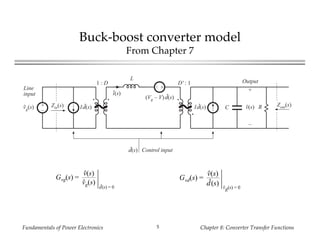
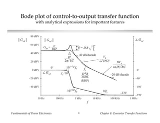
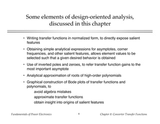
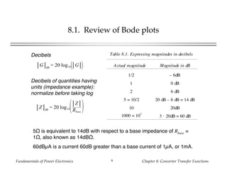
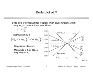
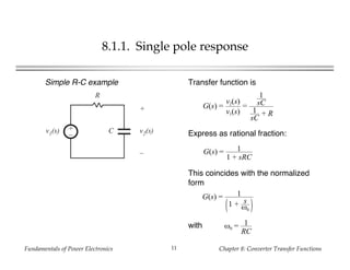
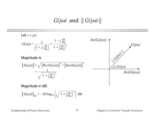
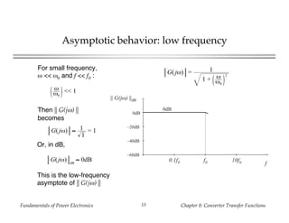
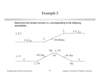
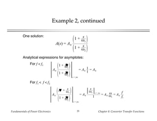
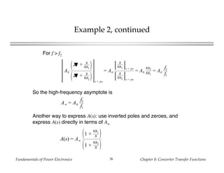
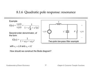
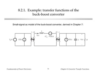
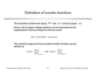
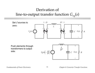
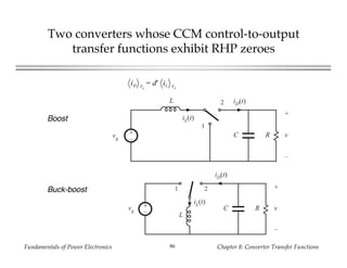
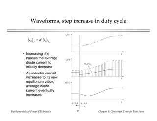
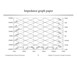
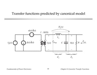
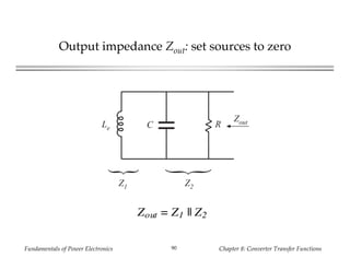
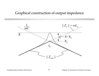
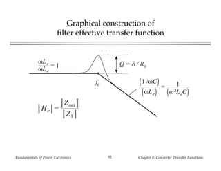
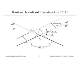
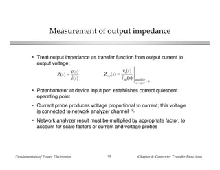
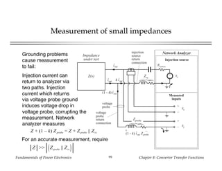
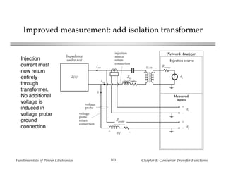
Fundamentals of Power Electronics Chapter 8: Converter Transfer Functions1
Chapter 8. Converter Transfer Functions
8.1. Review of Bode plots
8.1.1. Single pole response
8.1.2. Single zero response
8.1.3. Right half-plane zero
8.1.4. Frequency inversion
8.1.5. Combinations
8.1.6. Double pole response: resonance
8.1.7. The low-Q approximation
8.1.8. Approximate roots of an arbitrary-degree polynomial
8.2. Analysis of converter transfer functions
8.2.1. Example: transfer functions of the buck-boost converter
8.2.2. Transfer functions of some basic CCM converters
8.2.3. Physical origins of the right half-plane zero in converters
Fundamentals of Power Electronics Chapter 8: Converter Transfer Functions2
Converter Transfer Functions
8.3. Graphical construction of converter transfer
functions
8.3.1. Series impedances: addition of asymptotes
8.3.2. Parallel impedances: inverse addition of asymptotes
8.3.3. Another example
8.3.4. Voltage divider transfer functions: division of asymptotes
8.4. Measurement of ac transfer functions and
impedances
8.5. Summary of key points
Fundamentals of Power Electronics Chapter 8: Converter Transfer Functions3
The Engineering Design Process
1. Specifications and other design goals are defined.
2. A circuit is proposed. This is a creative process that draws on the
physical insight and experience of the engineer.
3. The circuit is modeled. The converter power stage is modeled as
described in Chapter 7. Components and other portions of the system
are modeled as appropriate, often with vendor-supplied data.
4. Design-oriented analysis of the circuit is performed. This involves
development of equations that allow element values to be chosen such
that specifications and design goals are met. In addition, it may be
necessary for the engineer to gain additional understanding and
physical insight into the circuit behavior, so that the design can be
improved by adding elements to the circuit or by changing circuit
connections.
5. Model verification. Predictions of the model are compared to a
laboratory prototype, under nominal operating conditions. The model is
refined as necessary, so that the model predictions agree with
laboratory measurements.
Fundamentals of Power Electronics Chapter 8: Converter Transfer Functions4
Design Process
6. Worst-case analysis (or other reliability and production yield
analysis) of the circuit is performed. This involves quantitative
evaluation of the model performance, to judge whether
specifications are met under all conditions. Computer
simulation is well-suited to this task.
7. Iteration. The above steps are repeated to improve the design
until the worst-case behavior meets specifications, or until the
reliability and production yield are acceptably high.
This Chapter: steps 4, 5, and 6
Fundamentals of Power Electronics Chapter 8: Converter Transfer Functions5
Buck-boost converter model
From Chapter 7
+
–
+
–
L
RC
1 : D D' : 1
vg(s) Id(s) Id(s)
i(s)
+
v(s)
–
(Vg – V) d(s)
Zout(s)Zin(s)
d(s) Control input
Line
input
Output
Gvg(s) =
v(s)
vg(s)
d(s) = 0
Gvd(s) =
v(s)
d(s) vg(s) = 0
Fundamentals of Power Electronics Chapter 8: Converter Transfer Functions6
Bode plot of control-to-output transfer function
with analytical expressions for important features
f
0˚
–90˚
–180˚
–270˚
|| Gvd ||
Gd0 =
|| Gvd || ∠ Gvd
0 dBV
–20 dBV
–40 dBV
20 dBV
40 dBV
60 dBV
80 dBV
Q =
∠ Gvd
10-1/2Q
f0
101/2Q
f0
0˚
–20 dB/decade
–40 dB/decade
–270˚
fz /10
10fz
1 MHz10 Hz 100 Hz 1 kHz 10 kHz 100 kHz
f0
V
DD' D'R C
L
D'
2π LC
D'2
R
2πDL
(RHP)
fz
DVg
ω(D')3
RC
Vg
ω2D'LC
Fundamentals of Power Electronics Chapter 8: Converter Transfer Functions7
Design-oriented analysis
How to approach a real (and hence, complicated) system
Problems:
Complicated derivations
Long equations
Algebra mistakes
Design objectives:
Obtain physical insight which leads engineer to synthesis of a good design
Obtain simple equations that can be inverted, so that element values can
be chosen to obtain desired behavior. Equations that cannot be inverted
are useless for design!
Design-oriented analysis is a structured approach to analysis, which attempts to
avoid the above problems
Fundamentals of Power Electronics Chapter 8: Converter Transfer Functions8
Some elements of design-oriented analysis,
discussed in this chapter
• Writing transfer functions in normalized form, to directly expose salient
features
• Obtaining simple analytical expressions for asymptotes, corner
frequencies, and other salient features, allows element values to be
selected such that a given desired behavior is obtained
• Use of inverted poles and zeroes, to refer transfer function gains to the
most important asymptote
• Analytical approximation of roots of high-order polynomials
• Graphical construction of Bode plots of transfer functions and
polynomials, to
avoid algebra mistakes
approximate transfer functions
obtain insight into origins of salient features
Fundamentals of Power Electronics Chapter 8: Converter Transfer Functions9
8.1. Review of Bode plots
Decibels
G dB
= 20 log10 G
Table 8.1. Expressing magnitudes in decibels
Actual magnitude Magnitude in dB
1/2 – 6dB
1 0 dB
2 6 dB
5 = 10/2 20 dB – 6 dB = 14 dB
10 20dB
1000 = 103
3 ⋅ 20dB = 60 dB
Z dB
= 20 log10
Z
Rbase
Decibels of quantities having
units (impedance example):
normalize before taking log
5Ω is equivalent to 14dB with respect to a base impedance of Rbase =
1Ω, also known as 14dBΩ.
60dBµA is a current 60dB greater than a base current of 1µA, or 1mA.
Fundamentals of Power Electronics Chapter 8: Converter Transfer Functions10
Bode plot of fn
G =
f
f0
n
Bode plots are effectively log-log plots, which cause functions which
vary as fn to become linear plots. Given:
Magnitude in dB is
G dB
= 20 log10
f
f0
n
= 20n log10
f
f0
f
f0
– 2
f
f0
2
0dB
–20dB
–40dB
–60dB
20dB
40dB
60dB
f
log scale
f00.1f0 10f0
f
f0
f
f0
– 1
n = 1
n
=
2
n
=
–2
n = –120 dB/decade
40dB/decade
–20dB/decade
–40dB/decade
• Slope is 20n dB/decade
• Magnitude is 1, or 0dB, at
frequency f = f0
Fundamentals of Power Electronics Chapter 8: Converter Transfer Functions11
8.1.1. Single pole response
+
–
R
Cv1(s)
+
v2(s)
–
Simple R-C example Transfer function is
G(s) =
v2(s)
v1(s)
=
1
sC
1
sC
+ R
G(s) = 1
1 + sRC
Express as rational fraction:
This coincides with the normalized
form
G(s) = 1
1 + s
ω0
with ω0 = 1
RC
Fundamentals of Power Electronics Chapter 8: Converter Transfer Functions12
G(jω) and || G(jω) ||
Im(G(jω))
Re(G(jω))
G(jω)
||G
(jω)||
∠G(jω)
G(jω) = 1
1 + j ω
ω0
=
1 – j ω
ω0
1 + ω
ω0
2
G(jω) = Re (G(jω))
2
+ Im (G(jω))
2
= 1
1 + ω
ω0
2
Let s = jω:
Magnitude is
Magnitude in dB:
G(jω) dB
= – 20 log10 1 + ω
ω0
2
dB
Fundamentals of Power Electronics Chapter 8: Converter Transfer Functions13
Asymptotic behavior: low frequency
G(jω) = 1
1 + ω
ω0
2
ω
ω0
<< 1
G(jω) ≈ 1
1
= 1
G(jω) dB
≈ 0dB
f
f0
– 1
–20dB/decade
f
f00.1f0 10f0
0dB
–20dB
–40dB
–60dB
0dB
|| G(jω) ||dB
For small frequency,
ω << ω0 and f << f0 :
Then || G(jω) ||
becomes
Or, in dB,
This is the low-frequency
asymptote of || G(jω) ||
Fundamentals of Power Electronics Chapter 8: Converter Transfer Functions14
Asymptotic behavior: high frequency
G(jω) = 1
1 + ω
ω0
2
f
f0
– 1
–20dB/decade
f
f00.1f0 10f0
0dB
–20dB
–40dB
–60dB
0dB
|| G(jω) ||dB
For high frequency,
ω >> ω0 and f >> f0 :
Then || G(jω) ||
becomes
The high-frequency asymptote of || G(jω) || varies as f-1.
Hence, n = -1, and a straight-line asymptote having a
slope of -20dB/decade is obtained. The asymptote has
a value of 1 at f = f0 .
ω
ω0
>> 1
1 + ω
ω0
2
≈ ω
ω0
2
G(jω) ≈ 1
ω
ω0
2
=
f
f0
– 1
Fundamentals of Power Electronics Chapter 8: Converter Transfer Functions15
Deviation of exact curve near f = f0
Evaluate exact magnitude:
at f = f0:
G(jω0) = 1
1 +
ω0
ω0
2
= 1
2
G(jω0) dB
= – 20 log10 1 +
ω0
ω0
2
≈ – 3 dB
at f = 0.5f0 and 2f0 :
Similar arguments show that the exact curve lies 1dB below
the asymptotes.
Fundamentals of Power Electronics Chapter 8: Converter Transfer Functions16
Summary: magnitude
–20dB/decade
f
f0
0dB
–10dB
–20dB
–30dB
|| G(jω) ||dB
3dB1dB
0.5f0 1dB
2f0
Fundamentals of Power Electronics Chapter 8: Converter Transfer Functions17
Phase of G(jω)
G(jω) = 1
1 + j ω
ω0
=
1 – j ω
ω0
1 + ω
ω0
2
∠G(jω) = tan– 1
Im G(jω)
Re G(jω)
Im(G(jω))
Re(G(jω))
G(jω)||G
(jω)||
∠G(jω)
∠G(jω) = – tan– 1
ω
ω0
Fundamentals of Power Electronics Chapter 8: Converter Transfer Functions18
-90˚
-75˚
-60˚
-45˚
-30˚
-15˚
0˚
f
0.01f0 0.1f0 f0 10f0 100f0
∠G(jω)
f0
-45˚
0˚ asymptote
–90˚ asymptote
Phase of G(jω)
∠G(jω) = – tan– 1
ω
ω0
ω ∠G(jω)
0 0˚
ω0
–45˚
∞ –90˚
Fundamentals of Power Electronics Chapter 8: Converter Transfer Functions19
Phase asymptotes
Low frequency: 0˚
High frequency: –90˚
Low- and high-frequency asymptotes do not intersect
Hence, need a midfrequency asymptote
Try a midfrequency asymptote having slope identical to actual slope at
the corner frequency f0. One can show that the asymptotes then
intersect at the break frequencies
fa = f0 e– π / 2
≈ f0 / 4.81
fb = f0 eπ / 2
≈ 4.81 f0
Fundamentals of Power Electronics Chapter 8: Converter Transfer Functions20
Phase asymptotes
fa = f0 e– π / 2
≈ f0 / 4.81
fb = f0 eπ / 2
≈ 4.81 f0
-90˚
-75˚
-60˚
-45˚
-30˚
-15˚
0˚
f
0.01f0 0.1f0 f0 100f0
∠G(jω)
f0
-45˚
fa = f0 / 4.81
fb = 4.81 f0
Fundamentals of Power Electronics Chapter 8: Converter Transfer Functions21
Phase asymptotes: a simpler choice
-90˚
-75˚
-60˚
-45˚
-30˚
-15˚
0˚
f
0.01f0 0.1f0 f0 100f0
∠G(jω)
f0
-45˚
fa = f0 / 10
fb
= 10 f0
fa = f0 / 10
fb = 10 f0
Fundamentals of Power Electronics Chapter 8: Converter Transfer Functions22
Summary: Bode plot of real pole
0˚
∠G(jω)
f0
-45˚
f0 / 10
10 f0
-90˚
5.7˚
5.7˚
-45˚/decade
–20dB/decade
f0
|| G(jω) ||dB 3dB1dB
0.5f0 1dB
2f0
0dB
G(s) = 1
1 + s
ω0
Fundamentals of Power Electronics Chapter 8: Converter Transfer Functions23
8.1.2. Single zero response
G(s) = 1 + s
ω0
Normalized form:
G(jω) = 1 + ω
ω0
2
∠G(jω) = tan– 1
ω
ω0
Magnitude:
Use arguments similar to those used for the simple pole, to derive
asymptotes:
0dB at low frequency, ω << ω0
+20dB/decade slope at high frequency, ω >> ω0
Phase:
—with the exception of a missing minus sign, same as simple pole
Fundamentals of Power Electronics Chapter 8: Converter Transfer Functions24
Summary: Bode plot, real zero
0˚∠G(jω)
f0
45˚
f0
/ 10
10 f0 +90˚
5.7˚
5.7˚
+45˚/decade
+20dB/decade
f0
|| G(jω) ||dB
3dB1dB
0.5f0
1dB
2f0
0dB
G(s) = 1 + s
ω0
Fundamentals of Power Electronics Chapter 8: Converter Transfer Functions25
8.1.3. Right half-plane zero
Normalized form:
G(jω) = 1 + ω
ω0
2
Magnitude:
—same as conventional (left half-plane) zero. Hence, magnitude
asymptotes are identical to those of LHP zero.
Phase:
—same as real pole.
The RHP zero exhibits the magnitude asymptotes of the LHP zero,
and the phase asymptotes of the pole
G(s) = 1 – s
ω0
∠G(jω) = – tan– 1
ω
ω0
Fundamentals of Power Electronics Chapter 8: Converter Transfer Functions26
+20dB/decade
f0
|| G(jω) ||dB
3dB1dB
0.5f0
1dB
2f0
0dB
0˚
∠G(jω)
f0
-45˚
f0
/ 10
10 f0
-90˚
5.7˚
5.7˚
-45˚/decade
Summary: Bode plot, RHP zero
G(s) = 1 – s
ω0
Fundamentals of Power Electronics Chapter 8: Converter Transfer Functions27
8.1.4. Frequency inversion
Reversal of frequency axis. A useful form when describing mid- or
high-frequency flat asymptotes. Normalized form, inverted pole:
An algebraically equivalent form:
The inverted-pole format emphasizes the high-frequency gain.
G(s) = 1
1 +
ω0
s
G(s) =
s
ω0
1 + s
ω0
Fundamentals of Power Electronics Chapter 8: Converter Transfer Functions28
Asymptotes, inverted pole
0˚
∠G(jω)
f0
+45˚
f0 / 10
10 f0
+90˚
5.7˚
5.7˚
-45˚/decade
0dB
+20dB/decade
f0
|| G(jω) ||dB
3dB
1dB
0.5f0
1dB
2f0
G(s) = 1
1 +
ω0
s
Fundamentals of Power Electronics Chapter 8: Converter Transfer Functions29
Inverted zero
Normalized form, inverted zero:
An algebraically equivalent form:
Again, the inverted-zero format emphasizes the high-frequency gain.
G(s) = 1 +
ω0
s
G(s) =
1 + s
ω0
s
ω0
Fundamentals of Power Electronics Chapter 8: Converter Transfer Functions30
Asymptotes, inverted zero
0˚
∠G(jω)
f0
–45˚
f0 / 10
10 f0
–90˚
5.7˚
5.7˚
+45˚/decade
–20dB/decade
f0
|| G(jω) ||dB
3dB
1dB
0.5f0
1dB
2f0
0dB
G(s) = 1 +
ω0
s
Fundamentals of Power Electronics Chapter 8: Converter Transfer Functions31
8.1.5. Combinations
Suppose that we have constructed the Bode diagrams of two
complex-values functions of frequency, G1(ω) and G2(ω). It is desired
to construct the Bode diagram of the product, G3(ω) = G1(ω) G2(ω).
Express the complex-valued functions in polar form:
G1(ω) = R1(ω) ejθ1(ω)
G2(ω) = R2(ω) ejθ2(ω)
G3(ω) = R3(ω) ejθ3(ω)
The product G3(ω) can then be written
G3(ω) = G1(ω) G2(ω) = R1(ω) ejθ1(ω)
R2(ω) ejθ2(ω)
G3(ω) = R1(ω) R2(ω) ej(θ1(ω) + θ2(ω))
Fundamentals of Power Electronics Chapter 8: Converter Transfer Functions32
Combinations
G3(ω) = R1(ω) R2(ω) ej(θ1(ω) + θ2(ω))
The composite phase is
θ3(ω) = θ1(ω) + θ2(ω)
The composite magnitude is
R3(ω) = R1(ω) R2(ω)
R3(ω) dB
= R1(ω) dB
+ R2(ω) dB
Composite phase is sum of individual phases.
Composite magnitude, when expressed in dB, is sum of individual
magnitudes.
Fundamentals of Power Electronics Chapter 8: Converter Transfer Functions33
Example 1: G(s) =
G0
1 + s
ω1
1 + s
ω2
–40 dB/decade
f
|| G ||
∠ G
∠ G|| G ||
0˚
–45˚
–90˚
–135˚
–180˚
–60 dB
0 dB
–20 dB
–40 dB
20 dB
40 dB
f1
100 Hz
f2
2 kHz
G0 = 40 ⇒ 32 dB
–20 dB/decade
0 dB
f1
/10
10 Hz
f2
/10
200 Hz
10f1
1 kHz
10f2
20 kHz
0˚
–45˚/decade
–90˚/decade
–45˚/decade
1 Hz 10 Hz 100 Hz 1 kHz 10 kHz 100 kHz
with G0 = 40 ⇒ 32 dB, f1 = ω1/2π = 100 Hz, f2 = ω2/2π = 2 kHz
Fundamentals of Power Electronics Chapter 8: Converter Transfer Functions34
Example 2
|| A ||
∠ A
f1
f2
|| A0 ||dB
+20 dB/dec
f1
/10
10f1 f2 /10
10f2
–45˚/dec+45˚/dec
0˚
|| A∞ ||dB
0˚
–90˚
Determine the transfer function A(s) corresponding to the following
asymptotes:
Fundamentals of Power Electronics Chapter 8: Converter Transfer Functions35
Example 2, continued
One solution:
A(s) = A0
1 + s
ω1
1 + s
ω2
Analytical expressions for asymptotes:
For f < f1
A0
1 + s
ω1
➚
1 + s
ω2
➚
s = jω
= A0
1
1
= A0
For f1 < f < f2
A0
1➚ + s
ω1
1 + s
ω2
➚
s = jω
= A0
s
ω1 s = jω
1
= A0
ω
ω1
= A0
f
f1
Fundamentals of Power Electronics Chapter 8: Converter Transfer Functions36
Example 2, continued
For f > f2
A0
1➚ + s
ω1
1➚ + s
ω2
s = jω
= A0
s
ω1 s = jω
s
ω2 s = jω
= A0
ω2
ω1
= A0
f2
f1
So the high-frequency asymptote is
A∞ = A0
f2
f1
Another way to express A(s): use inverted poles and zeroes, and
express A(s) directly in terms of A∞
A(s) = A∞
1 +
ω1
s
1 +
ω2
s
Fundamentals of Power Electronics Chapter 8: Converter Transfer Functions37
8.1.6 Quadratic pole response: resonance
+
–
L
C Rv1(s)
+
v2(s)
–
Two-pole low-pass filter example
Example
G(s) =
v2(s)
v1(s)
= 1
1 + sL
R
+ s2
LC
Second-order denominator, of
the form
G(s) = 1
1 + a1s + a2s2
with a1 = L/R and a2 = LC
How should we construct the Bode diagram?
Fundamentals of Power Electronics Chapter 8: Converter Transfer Functions38
Approach 1: factor denominator
G(s) = 1
1 + a1s + a2s2
We might factor the denominator using the quadratic formula, then
construct Bode diagram as the combination of two real poles:
G(s) = 1
1 – s
s1
1 – s
s2
with s1 = –
a1
2a2
1 – 1 –
4a2
a1
2
s2 = –
a1
2a2
1 + 1 –
4a2
a1
2
• If 4a2 ≤ a1
2, then the roots s1 and s2 are real. We can construct Bode
diagram as the combination of two real poles.
• If 4a2 > a1
2, then the roots are complex. In Section 8.1.1, the
assumption was made that ω0 is real; hence, the results of that
section cannot be applied and we need to do some additional work.
Fundamentals of Power Electronics Chapter 8: Converter Transfer Functions39
Approach 2: Define a standard normalized form
for the quadratic case
G(s) = 1
1 + 2ζ s
ω0
+ s
ω0
2 G(s) = 1
1 + s
Qω0
+ s
ω0
2or
• When the coefficients of s are real and positive, then the parameters ζ,
ω0, and Q are also real and positive
• The parameters ζ, ω0, and Q are found by equating the coefficients of s
• The parameter ω0 is the angular corner frequency, and we can define f0
= ω0/2π
• The parameter ζ is called the damping factor. ζ controls the shape of the
exact curve in the vicinity of f = f0. The roots are complex when ζ < 1.
• In the alternative form, the parameter Q is called the quality factor. Q
also controls the shape of the exact curve in the vicinity of f = f0. The
roots are complex when Q > 0.5.
Fundamentals of Power Electronics Chapter 8: Converter Transfer Functions40
The Q-factor
Q = 1
2ζ
In a second-order system, ζ and Q are related according to
Q is a measure of the dissipation in the system. A more general
definition of Q, for sinusoidal excitation of a passive element or system
is
Q = 2π
(peak stored energy)
(energy dissipated per cycle)
For a second-order passive system, the two equations above are
equivalent. We will see that Q has a simple interpretation in the Bode
diagrams of second-order transfer functions.
Fundamentals of Power Electronics Chapter 8: Converter Transfer Functions41
Analytical expressions for f0 and Q
G(s) =
v2(s)
v1(s)
= 1
1 + sL
R
+ s2
LC
Two-pole low-pass filter
example: we found that
G(s) = 1
1 + s
Qω0
+ s
ω0
2
Equate coefficients of like
powers of s with the
standard form
Result:
f0 =
ω0
2π
= 1
2π LC
Q = R C
L
Fundamentals of Power Electronics Chapter 8: Converter Transfer Functions42
Magnitude asymptotes, quadratic form
G(jω) = 1
1 – ω
ω0
2 2
+ 1
Q2
ω
ω0
2
G(s) = 1
1 + s
Qω0
+ s
ω0
2
In the form
let s = jω and find magnitude:
Asymptotes are
G → 1 for ω << ω0
G →
f
f0
– 2
for ω >> ω0
f
f0
– 2
–40 dB/decade
f
f00.1f0 10f0
0 dB
|| G(jω) ||dB
0 dB
–20 dB
–40 dB
–60 dB
Fundamentals of Power Electronics Chapter 8: Converter Transfer Functions43
Deviation of exact curve from magnitude asymptotes
G(jω) = 1
1 – ω
ω0
2 2
+ 1
Q2
ω
ω0
2
At ω = ω0, the exact magnitude is
G(jω0) = Q G(jω0) dB
= Q dBor, in dB:
The exact curve has magnitude
Q at f = f0. The deviation of the
exact curve from the
asymptotes is | Q |dB
|| G ||
f0
| Q |dB0 dB
–40 dB/decade
Fundamentals of Power Electronics Chapter 8: Converter Transfer Functions44
Two-pole response: exact curves
Q = ∞
Q = 5
Q = 2
Q = 1
Q = 0.7
Q = 0.5
Q = 0.2
Q = 0.1
-20dB
-10dB
0dB
10dB
10.3 0.5 2 30.7
f / f0
|| G ||dB
Q = 0.1
Q = 0.5
Q = 0.7
Q = 1
Q = 2
Q =5
Q = 10
Q = ∞
-180°
-135°
-90°
-45°
0°
0.1 1 10
f / f0
∠G
Q = 0.2
Fundamentals of Power Electronics Chapter 8: Converter Transfer Functions45
8.1.7. The low-Q approximation
G(s) = 1
1 + a1s + a2s2 G(s) = 1
1 + s
Qω0
+ s
ω0
2
Given a second-order denominator polynomial, of the form
or
When the roots are real, i.e., when Q < 0.5, then we can factor the
denominator, and construct the Bode diagram using the asymptotes
for real poles. We would then use the following normalized form:
G(s) = 1
1 + s
ω1
1 + s
ω2
This is a particularly desirable approach when Q << 0.5, i.e., when the
corner frequencies ω1 and ω2 are well separated.
Fundamentals of Power Electronics Chapter 8: Converter Transfer Functions46
An example
A problem with this procedure is the complexity of the quadratic
formula used to find the corner frequencies.
R-L-C network example:
+
–
L
C Rv1(s)
+
v2(s)
–
G(s) =
v2(s)
v1(s)
= 1
1 + sL
R
+ s2
LC
Use quadratic formula to factor denominator. Corner frequencies are:
ω1, ω2 =
L / R ± L / R
2
– 4 LC
2 LC
Fundamentals of Power Electronics Chapter 8: Converter Transfer Functions47
Factoring the denominator
ω1, ω2 =
L / R ± L / R
2
– 4 LC
2 LC
This complicated expression yields little insight into how the corner
frequencies ω1 and ω2 depend on R, L, and C.
When the corner frequencies are well separated in value, it can be
shown that they are given by the much simpler (approximate)
expressions
ω1 ≈ R
L
, ω2 ≈ 1
RC
ω1 is then independent of C, and ω2 is independent of L.
These simpler expressions can be derived via the Low-Q Approximation.
Fundamentals of Power Electronics Chapter 8: Converter Transfer Functions48
Derivation of the Low-Q Approximation
G(s) = 1
1 + s
Qω0
+ s
ω0
2
Given
Use quadratic formula to express corner frequencies ω1 and ω2 in
terms of Q and ω0 as:
ω1 =
ω0
Q
1 – 1 – 4Q2
2
ω2 =
ω0
Q
1 + 1 – 4Q2
2
Fundamentals of Power Electronics Chapter 8: Converter Transfer Functions49
Corner frequency ω2
ω2 =
ω0
Q
1 + 1 – 4Q2
2
ω2 =
ω0
Q
F(Q)
F(Q) = 1
2
1 + 1 – 4Q2
ω2 ≈
ω0
Q
for Q << 1
2
F(Q)
0 0.1 0.2 0.3 0.4 0.5
Q
0
0.25
0.5
0.75
1
can be written in the form
where
For small Q, F(Q) tends to 1.
We then obtain
For Q < 0.3, the approximation F(Q) = 1 is
within 10% of the exact value.
Fundamentals of Power Electronics Chapter 8: Converter Transfer Functions50
Corner frequency ω1
F(Q) = 1
2
1 + 1 – 4Q2
F(Q)
0 0.1 0.2 0.3 0.4 0.5
Q
0
0.25
0.5
0.75
1
can be written in the form
where
For small Q, F(Q) tends to 1.
We then obtain
For Q < 0.3, the approximation F(Q) = 1 is
within 10% of the exact value.
ω1 =
ω0
Q
1 – 1 – 4Q2
2
ω1 =
Q ω0
F(Q)
ω1 ≈ Q ω0 for Q << 1
2
Fundamentals of Power Electronics Chapter 8: Converter Transfer Functions51
The Low-Q Approximation
f2 =
f0F(Q)
Q
≈
f0
Q
–40dB/decade
f0
0dB
|| G ||dB
–20dB/decade
f1 =
Qf0
F(Q)
≈ Qf0
Fundamentals of Power Electronics Chapter 8: Converter Transfer Functions52
R-L-C Example
ω1 ≈ Q ω0 = R C
L
1
LC
= R
L
ω2 ≈
ω0
Q
= 1
LC
1
R C
L
= 1
RC
G(s) =
v2(s)
v1(s)
= 1
1 + sL
R
+ s2
LC
f0 =
ω0
2π
= 1
2π LC
Q = R C
L
For the previous example:
Use of the Low-Q Approximation leads to
Fundamentals of Power Electronics Chapter 8: Converter Transfer Functions53
8.1.8. Approximate Roots of an
Arbitrary-Degree Polynomial
Generalize the low-Q approximation to obtain approximate
factorization of the nth-order polynomial
P(s) = 1 + a1 s + a2 s2
+ + an sn
It is desired to factor this polynomial in the form
P(s) = 1 + τ1 s 1 + τ2 s 1 + τn s
When the roots are real and well separated in value, then approximate
analytical expressions for the time constants τ1, τ2, ... τn can be found,
that typically are simple functions of the circuit element values.
Objective: find a general method for deriving such expressions.
Include the case of complex root pairs.
Fundamentals of Power Electronics Chapter 8: Converter Transfer Functions54
Derivation of method
Multiply out factored form of polynomial, then equate to original form
(equate like powers of s):
a1 = τ1 + τ2 + + τn
a2 = τ1 τ2 + + τn + τ2 τ3 + + τn +
a3 = τ1τ2 τ3 + + τn + τ2τ3 τ4 + + τn +
an = τ1τ2τ3 τn
• Exact system of equations relating roots to original coefficients
• Exact general solution is hopeless
• Under what conditions can solution for time constants be easily
approximated?
Fundamentals of Power Electronics Chapter 8: Converter Transfer Functions55
Approximation of time constants
when roots are real and well separated
a1 = τ1 + τ2 + + τn
a2 = τ1 τ2 + + τn + τ2 τ3 + + τn +
a3 = τ1τ2 τ3 + + τn + τ2τ3 τ4 + + τn +
an = τ1τ2τ3 τn
System of equations:
(from previous slide)
Suppose that roots are real and well-separated, and are arranged in
decreasing order of magnitude:
τ1 >> τ2 >> >> τn
Then the first term of each equation is dominant
⇒ Neglect second and following terms in each equation above
Fundamentals of Power Electronics Chapter 8: Converter Transfer Functions56
Approximation of time constants
when roots are real and well separated
System of equations:
(only first term in each
equation is included)
a1 ≈ τ1
a2 ≈ τ1τ2
a3 ≈ τ1τ2τ3
an = τ1τ2τ3 τn
Solve for the time
constants:
τ1 ≈ a1
τ2 ≈
a2
a1
τ3 ≈
a3
a2
τn ≈
an
an – 1
Fundamentals of Power Electronics Chapter 8: Converter Transfer Functions57
Result
when roots are real and well separated
If the following inequalities are satisfied
a1 >>
a2
a1
>>
a3
a2
>> >>
an
an – 1
Then the polynomial P(s) has the following approximate factorization
P(s) ≈ 1 + a1 s 1 +
a2
a1
s 1 +
a3
a2
s 1 +
an
an – 1
s
• If the an coefficients are simple analytical functions of the element
values L, C, etc., then the roots are similar simple analytical
functions of L, C, etc.
• Numerical values are used to justify the approximation, but
analytical expressions for the roots are obtained
Fundamentals of Power Electronics Chapter 8: Converter Transfer Functions58
When two roots are not well separated
then leave their terms in quadratic form
Suppose inequality k is not satisfied:
a1 >>
a2
a1
>> >>
ak
ak – 1
>>✖
ak + 1
ak
>> >>
an
an – 1
↑
not
satisfied
Then leave the terms corresponding to roots k and (k + 1) in quadratic
form, as follows:
P(s) ≈ 1 + a1 s 1 +
a2
a1
s 1 +
ak
ak – 1
s +
ak + 1
ak – 1
s2
1 +
an
an – 1
s
This approximation is accurate provided
a1 >>
a2
a1
>> >>
ak
ak – 1
>>
ak – 2 ak + 1
ak – 1
2
>>
ak + 2
ak + 1
>> >>
an
an – 1
Fundamentals of Power Electronics Chapter 8: Converter Transfer Functions59
When the first inequality is violated
A special case for quadratic roots
a1 >>✖
a2
a1
>>
a3
a2
>> >>
an
an – 1
↑
not
satisfied
When inequality 1 is not satisfied:
Then leave the first two roots in quadratic form, as follows:
This approximation is justified provided
P(s) ≈ 1 + a1s + a2s2
1 +
a3
a2
s 1 +
an
an – 1
s
a2
2
a3
>> a1 >>
a3
a2
>>
a4
a3
>> >>
an
an – 1
Fundamentals of Power Electronics Chapter 8: Converter Transfer Functions60
Other cases
• When several isolated inequalities are violated
—Leave the corresponding roots in quadratic form
—See next two slides
• When several adjacent inequalities are violated
—Then the corresponding roots are close in value
—Must use cubic or higher-order roots
Fundamentals of Power Electronics Chapter 8: Converter Transfer Functions61
Leaving adjacent roots in quadratic form
a1 >
a2
a1
> >
ak
ak – 1
≥
ak + 1
ak
> >
an
an – 1
In the case when inequality k is not satisfied:
P(s) ≈ 1 + a1 s 1 +
a2
a1
s 1 +
ak
ak – 1
s +
ak + 1
ak – 1
s2 1 +
an
an – 1
s
Then leave the corresponding roots in quadratic form:
This approximation is accurate provided that
a1 >
a2
a1
> >
ak
ak – 1
>
ak – 2 ak + 1
ak – 1
2 >
ak + 2
ak + 1
> >
an
an – 1
(derivation is similar to the case of well-separated roots)
Fundamentals of Power Electronics Chapter 8: Converter Transfer Functions62
When the first inequality is not satisfied
The formulas of the previous slide require a special form for the case when
the first inequality is not satisfied:
a1 ≥
a2
a1
>
a3
a2
> >
an
an – 1
P(s) ≈ 1 + a1s + a2s2 1 +
a3
a2
s 1 +
an
an – 1
s
We should then use the following form:
a2
2
a3
> a1 >
a3
a2
>
a4
a3
> >
an
an – 1
The conditions for validity of this approximation are:
Fundamentals of Power Electronics Chapter 8: Converter Transfer Functions63
Example
Damped input EMI filter
+
–
vg
ig ic
C
R
L1
L2 Converter
G(s) =
ig(s)
ic(s)
=
1 + s
L1 + L2
R
1 + s
L1 + L2
R
+ s2L1C + s3 L1L2C
R
Fundamentals of Power Electronics Chapter 8: Converter Transfer Functions64
Example
Approximate factorization of a third-order denominator
The filter transfer function from the previous slide is
—contains a third-order denominator, with the following coefficients:
a1 =
L1 + L2
R
a2 = L1C
a3 =
L1L2C
R
G(s) =
ig(s)
ic(s)
=
1 + s
L1 + L2
R
1 + s
L1 + L2
R
+ s2L1C + s3 L1L2C
R
Fundamentals of Power Electronics Chapter 8: Converter Transfer Functions65
Real roots case
Factorization as three real roots:
1 + s
L1 + L2
R
1 + sRC
L1
L1 + L2
1 + s
L2
R
This approximate analytical factorization is justified provided
L1 + L2
R
>> RC
L1
L1 + L2
>>
L2
R
Note that these inequalities cannot be satisfied unless L1 >> L2. The
above inequalities can then be further simplified to
L1
R
>> RC >>
L2
R
And the factored polynomial reduces to
1 + s
L1
R
1 + sRC 1 + s
L2
R
• Illustrates in a simple
way how the roots
depend on the
element values
Fundamentals of Power Electronics Chapter 8: Converter Transfer Functions66
When the second inequality is violated
L1 + L2
R
>> RC
L1
L1 + L2
>>✖
L2
R
↑
not
satisfied
Then leave the second and third roots in quadratic form:
1 + s
L1 + L2
R
1 + sRC
L1
L1 + L2
+ s2
L1||L2 C
P(s) = 1 + a1s 1 +
a2
a1
s +
a3
a1
s2
which is
Fundamentals of Power Electronics Chapter 8: Converter Transfer Functions67
Validity of the approximation
This is valid provided
L1 + L2
R
>> RC
L1
L1 + L2
>>
L1||L2
L1 + L2
RC (use a0 = 1)
These inequalities are equivalent to
L1 >> L2, and
L1
R
>> RC
It is no longer required that RC >> L2/R
The polynomial can therefore be written in the simplified form
1 + s
L1
R
1 + sRC + s2
L2C
Fundamentals of Power Electronics Chapter 8: Converter Transfer Functions68
When the first inequality is violated
Then leave the first and second roots in quadratic form:
which is
L1 + L2
R
>>✖ RC
L1
L1 + L2
>>
L2
R
↑
not
satisfied
1 + s
L1 + L2
R
+ s2
L1C 1 + s
L2
R
P(s) = 1 + a1s + a2s2
1 +
a3
a2
s
Fundamentals of Power Electronics Chapter 8: Converter Transfer Functions69
Validity of the approximation
This is valid provided
These inequalities are equivalent to
It is no longer required that L1/R >> RC
The polynomial can therefore be written in the simplified form
L1RC
L2
>>
L1 + L2
R
>>
L2
R
L1 >> L2, and RC >>
L2
R
1 + s
L1
R
+ s2
L1C 1 + s
L2
R
Fundamentals of Power Electronics Chapter 8: Converter Transfer Functions70
8.2. Analysis of converter transfer functions
8.2.1. Example: transfer functions of the buck-boost converter
8.2.2. Transfer functions of some basic CCM converters
8.2.3. Physical origins of the right half-plane zero in converters
Fundamentals of Power Electronics Chapter 8: Converter Transfer Functions71
8.2.1. Example: transfer functions of the
buck-boost converter
Small-signal ac model of the buck-boost converter, derived in Chapter 7:
+
–
+
–
L
RC
1 : D D' : 1
vg(s) I d(s) Id(s)
i(s)
(Vg – V)d(s)
+
v(s)
–
Fundamentals of Power Electronics Chapter 8: Converter Transfer Functions72
Definition of transfer functions
The converter contains two inputs, and and one output,
Hence, the ac output voltage variations can be expressed as the
superposition of terms arising from the two inputs:
v(s) = Gvd(s) d(s) + Gvg(s) vg(s)
d(s) vg(s) v(s)
The control-to-output and line-to-output transfer functions can be
defined as
Gvd(s) =
v(s)
d(s) vg(s) = 0
and Gvg(s) =
v(s)
vg(s) d(s) = 0
Fundamentals of Power Electronics Chapter 8: Converter Transfer Functions73
Derivation of
line-to-output transfer function Gvg(s)
+
–
L
RC
1 : D D' : 1
vg(s)
+
v(s)
–
Set d sources to
zero:
+
– RC
+
v(s)
–
L
D'2
vg(s) – D
D'
Push elements through
transformers to output
side:
Fundamentals of Power Electronics Chapter 8: Converter Transfer Functions74
Derivation of transfer functions
+
– RC
+
v(s)
–
L
D'2
vg(s) – D
D'
Use voltage divider formula
to solve for transfer function:
Gvg(s) =
v(s)
vg(s)
d(s) = 0
= – D
D'
R || 1
sC
sL
D'2 + R || 1
sC
Expand parallel combination and express as a rational fraction:
Gvg(s) = – D
D'
R
1 + sRC
sL
D'2 + R
1 + sRC
= – D
D'
R
R + sL
D'2 + s2RLC
D'2
We aren’t done yet! Need to
write in normalized form, where
the coefficient of s0 is 1, and
then identify salient features
Fundamentals of Power Electronics Chapter 8: Converter Transfer Functions75
Derivation of transfer functions
Divide numerator and denominator by R. Result: the line-to-output
transfer function is
Gvg(s) =
v(s)
vg(s) d(s) = 0
= – D
D'
1
1 + s L
D'2
R
+ s2 LC
D'2
which is of the following standard form:
Gvg(s) = Gg0
1
1 + s
Qω0
+ s
ω0
2
Fundamentals of Power Electronics Chapter 8: Converter Transfer Functions76
Salient features of the line-to-output transfer function
Gg0 = – D
D'
Equate standard form to derived transfer function, to determine
expressions for the salient features:
1
ω0
2 = LC
D'2 ω0 = D'
LC
1
Qω0
= L
D'2
R Q = D'R C
L
Fundamentals of Power Electronics Chapter 8: Converter Transfer Functions77
Derivation of
control-to-output transfer function Gvd(s)
+
–
L
RC
D' : 1
I d(s)
(Vg – V) d(s)
+
v(s)
–
In small-signal model,
set vg source to zero:
+
–
RCId(s)
+
v(s)
–
L
D'2
Vg – V
D'
d(s)
Push all elements to
output side of
transformer:
There are two d sources. One way to solve the model is to use superposition,
expressing the output v as a sum of terms arising from the two sources.
Fundamentals of Power Electronics Chapter 8: Converter Transfer Functions78
Superposition
+
–
RC
+
v(s)
–
L
D'2
Vg – V
D'
d(s)
RCI d(s)
+
v(s)
–
L
D'2
v(s)
d(s)
= –
Vg – V
D'
R || 1
sC
sL
D'2 + R || 1
sC
With the voltage
source only:
With the current
source alone: v(s)
d(s)
= I sL
D'2 || R || 1
sC
Total: Gvd(s) = –
Vg – V
D'
R || 1
sC
sL
D'2 + R || 1
sC
+ I sL
D'2 || R || 1
sC
Fundamentals of Power Electronics Chapter 8: Converter Transfer Functions79
Control-to-output transfer function
Gvd(s) =
v(s)
d(s) vg(s) = 0
= –
Vg – V
D'2
1 – s LI
Vg – V
1 + s L
D'2
R
+ s2 LC
D'2
This is of the following standard form:
Gvd(s) = Gd0
1 – s
ωz
1 + s
Qω0
+ s
ω0
2
Express in normalized form:
Fundamentals of Power Electronics Chapter 8: Converter Transfer Functions80
Salient features of control-to-output transfer function
ωz =
Vg – V
L I
= D' R
D L
(RHP)
ω0 = D'
LC
Q = D'R C
L
V = – D
D'
Vg
I = – V
D' R
— Simplified using the dc relations:
Gd0 = –
Vg – V
D'
= –
Vg
D'2 = V
DD'
Fundamentals of Power Electronics Chapter 8: Converter Transfer Functions81
Plug in numerical values
Suppose we are given the
following numerical values:
D = 0.6
R = 10Ω
Vg = 30V
L = 160µH
C = 160µF
Then the salient features
have the following numerical
values:
Gg0 = D
D'
= 1.5 ⇒ 3.5 dB
Gd0 =
V
DD'
= 187.5 V ⇒ 45.5 dBV
f0 =
ω0
2π
= D'
2π LC
= 400 Hz
Q = D'R C
L
= 4 ⇒ 12 dB
fz =
ωz
2π
= D'2
R
2πDL
= 2.65 kHz
Fundamentals of Power Electronics Chapter 8: Converter Transfer Functions82
Bode plot: control-to-output transfer function
f
0˚
–90˚
–180˚
–270˚
|| Gvd ||
Gd0
= 187 V
⇒ 45.5 dBV
|| Gvd || ∠ Gvd
0 dBV
–20 dBV
–40 dBV
20 dBV
40 dBV
60 dBV
80 dBV
Q = 4 ⇒ 12 dB
fz
2.6 kHz
RHP
∠ Gvd
10-1/2Q
f0
101/2Q
f0
0˚ 300 Hz
533 Hz
–20 dB/decade
–40 dB/decade
–270˚
fz
/10
260 Hz
10fz
26 kHz
1 MHz10 Hz 100 Hz 1 kHz 10 kHz 100 kHz
f0
400 Hz
Fundamentals of Power Electronics Chapter 8: Converter Transfer Functions83
Bode plot: line-to-output transfer function
f
|| Gvg ||
|| Gvg ||
∠ Gvg
10–1/2Q0 f0
101/2Q0 f0
0˚ 300 Hz
533 Hz
–180˚
–60 dB
–80 dB
–40 dB
–20 dB
0 dB
20 dB
Gg0
= 1.5
⇒ 3.5 dB
f0
Q = 4 ⇒ 12 dB
400 Hz –40 dB/decade
0˚
–90˚
–180˚
–270˚
∠ Gvg
10 Hz 100 Hz 1 kHz 10 kHz 100 kHz
Fundamentals of Power Electronics Chapter 8: Converter Transfer Functions84
8.2.2. Transfer functions of
some basic CCM converters
Table 8.2. Salient features of the small-signal CCM transfer functions of some basic dc-dc converters
Converter Gg0 Gd0 ω0 Q ωz
buck D
V
D
1
LC
R C
L ∞
boost
1
D'
V
D'
D'
LC
D'R C
L
D'2
R
L
buck-boost – D
D'
V
D D'
2
D'
LC
D'R C
L
D'2
R
D L
where the transfer functions are written in the standard forms
Gvd(s) = Gd0
1 – s
ωz
1 + s
Qω0
+ s
ω0
2
Gvg(s) = Gg0
1
1 + s
Qω0
+ s
ω0
2
Fundamentals of Power Electronics Chapter 8: Converter Transfer Functions85
8.2.3. Physical origins of the right half-plane zero
G(s) = 1 – s
ω0
• phase reversal at
high frequency
• transient response:
output initially tends
in wrong direction
+
–
1
s
ωz
uout(s)uin(s)
Fundamentals of Power Electronics Chapter 8: Converter Transfer Functions86
Two converters whose CCM control-to-output
transfer functions exhibit RHP zeroes
Boost
Buck-boost
iD Ts
= d' iL Ts
+
–
L
C R
+
v
–
1
2
vg
iL(t)
iD(t)
+
– L
C R
+
v
–
1 2
vg
iL(t)
iD(t)
Fundamentals of Power Electronics Chapter 8: Converter Transfer Functions87
Waveforms, step increase in duty cycle
iD Ts
= d' iL Ts
• Increasing d(t)
causes the average
diode current to
initially decrease
• As inductor current
increases to its new
equilibrium value,
average diode
current eventually
increases
t
iD(t)
〈iD(t)〉Ts
t
| v(t) |
t
iL(t)
d = 0.6d = 0.4
Fundamentals of Power Electronics Chapter 8: Converter Transfer Functions88
Impedance graph paper
10Ω
1Ω
100mΩ
100Ω
1kΩ
10kΩ
10mΩ
1mΩ
100µH
1mH
10µH 100nH
10nH
1nH
10Hz 100Hz 1kHz 10kHz 100kHz 1MHz
1µH
10mH
100mH
1H
10H
10µF
100µF1mF
10mF
100mF
1F
1µF
100nF
10nF
1nF
100pF
20dBΩ
0dBΩ
–20dBΩ
40dBΩ
60dBΩ
80dBΩ
–40dBΩ
–60dBΩ
Fundamentals of Power Electronics Chapter 8: Converter Transfer Functions89
Transfer functions predicted by canonical model
+
–
+
–
1 : M(D)
Le
C Rvg(s)
e(s) d(s)
j(s) d(s)
+
–
v(s)
+
–
ve(s)
He(s)
Zout
Z2Z1
{
{
Zin
Fundamentals of Power Electronics Chapter 8: Converter Transfer Functions90
Output impedance Zout: set sources to zero
Le C R
Zout
Z2Z1
{
{Zout = Z1 || Z2
Fundamentals of Power Electronics Chapter 8: Converter Transfer Functions91
Graphical construction of output impedance
1
ωC
R
|| Zout ||
f0
R0
|| Z1 || = ωLe
Q = R / R0
Fundamentals of Power Electronics Chapter 8: Converter Transfer Functions92
Graphical construction of
filter effective transfer function
f0
Q = R / R0
ωLe
ωLe
= 1
1 /ωC
ωLe
= 1
ω2LeC
He =
Zout
Z1
Fundamentals of Power Electronics Chapter 8: Converter Transfer Functions93
Boost and buck-boost converters: Le = L / D’ 2
1
ωC
R
|| Zout ||
f0
R0
Q = R / R0
ωL
D'2
increasing
D
Fundamentals of Power Electronics Chapter 8: Converter Transfer Functions94
8.4. Measurement of ac transfer functions
and impedances
Network Analyzer
Injection source Measured inputs
vy
magnitude
vz
frequency
vz
output
vz
+
–
input
vx
input
+ – + –
vy
vx
vy
vx
Data
17.3 dB
– 134.7˚
Data bus
to computer
Fundamentals of Power Electronics Chapter 8: Converter Transfer Functions95
Swept sinusoidal measurements
• Injection source produces sinusoid of controllable amplitude and
frequency
• Signal inputs and perform function of narrowband tracking
voltmeter:
Component of input at injection source frequency is measured
Narrowband function is essential: switching harmonics and other
noise components are removed
• Network analyzer measures
vz
vx vy
∠
vy
vx
vy
vx
and
Fundamentals of Power Electronics Chapter 8: Converter Transfer Functions96
Measurement of an ac transfer function
Network Analyzer
Injection source Measured inputs
vy
magnitude
vz
frequency
vz
output
vz
+
–
input
vx
input
+ – + –
vy
vx
vy
vx
Data
–4.7 dB
– 162.8˚
Data bus
to computer
Device
under test
G(s)
input
output
VCC
DC
bias
adjust
DC
blocking
capacitor
• Potentiometer
establishes correct
quiescent operating
point
• Injection sinusoid
coupled to device
input via dc blocking
capacitor
• Actual device input
and output voltages
are measured as
and
• Dynamics of blocking
capacitor are irrelevant
vx
vy
vy(s)
vx(s)
= G(s)
Fundamentals of Power Electronics Chapter 8: Converter Transfer Functions97
Measurement of an output impedance
Z(s) =
v(s)
i(s)
VCC
DC
bias
adjust
Device
under test
G(s)
input
output
Zout +
– vz
iout
vy
+ –
voltage
probe
Zs
{
Rsource
DC blocking
capacitor
current
probe
vx
+ –
Zout(s) =
vy(s)
iout(s) amplifier
ac input
= 0
Fundamentals of Power Electronics Chapter 8: Converter Transfer Functions98
Measurement of output impedance
• Treat output impedance as transfer function from output current to
output voltage:
• Potentiometer at device input port establishes correct quiescent
operating point
• Current probe produces voltage proportional to current; this voltage
is connected to network analyzer channel
• Network analyzer result must be multiplied by appropriate factor, to
account for scale factors of current and voltage probes
vx
Z(s) =
v(s)
i(s)
Zout(s) =
vy(s)
iout(s) amplifier
ac input
= 0
Fundamentals of Power Electronics Chapter 8: Converter Transfer Functions99
Measurement of small impedances
Impedance
under test
Z(s) +
– vz
iout
vy
+
–
voltage
probe
Rsource
vx
+
–
Network Analyzer
Injection source
Measured
inputs
voltage
probe
return
connection
injection
source
return
connection
iout
Zrz
{
{
Zprobe
k iout
(1 – k) iout
+ –
(1 – k) iout Zprobe
Grounding problems
cause measurement
to fail:
Injection current can
return to analyzer via
two paths. Injection
current which returns
via voltage probe ground
induces voltage drop in
voltage probe, corrupting the
measurement. Network
analyzer measures
Z + (1 – k) Zprobe = Z + Zprobe || Zrz
For an accurate measurement, require
Z >> Zprobe || Zrz
Fundamentals of Power Electronics Chapter 8: Converter Transfer Functions100
Improved measurement: add isolation transformer
Impedance
under test
Z(s) +
– vz
iout
vy
+
–
voltage
probe
Rsource
vx
+
–
Network Analyzer
Injection source
Measured
inputs
voltage
probe
return
connection
injection
source
return
connection
Zrz
{
{Zprobe
+ –0V
0
iout
1 : n
Injection
current must
now return
entirely
through
transformer.
No additional
voltage is
induced in
voltage probe
ground
connection
Fundamentals of Power Electronics Chapter 8: Converter Transfer Functions101
8.5. Summary of key points
1. The magnitude Bode diagrams of functions which vary as (f / f0)n
have slopes equal to 20n dB per decade, and pass through 0dB at
f = f0.
2. It is good practice to express transfer functions in normalized pole-
zero form; this form directly exposes expressions for the salient
features of the response, i.e., the corner frequencies, reference
gain, etc.
3. The right half-plane zero exhibits the magnitude response of the
left half-plane zero, but the phase response of the pole.
4. Poles and zeroes can be expressed in frequency-inverted form,
when it is desirable to refer the gain to a high-frequency asymptote.
Fundamentals of Power Electronics Chapter 8: Converter Transfer Functions102
Summary of key points
5. A two-pole response can be written in the standard normalized
form of Eq. (8-53). When Q > 0.5, the poles are complex
conjugates. The magnitude response then exhibits peaking in the
vicinity of the corner frequency, with an exact value of Q at f = f0.
High Q also causes the phase to change sharply near the corner
frequency.
6. When the Q is less than 0.5, the two pole response can be plotted
as two real poles. The low- Q approximation predicts that the two
poles occur at frequencies f0 / Q and Qf0. These frequencies are
within 10% of the exact values for Q ≤ 0.3.
7. The low- Q approximation can be extended to find approximate
roots of an arbitrary degree polynomial. Approximate analytical
expressions for the salient features can be derived. Numerical
values are used to justify the approximations.
Fundamentals of Power Electronics Chapter 8: Converter Transfer Functions103
Summary of key points
8. Salient features of the transfer functions of the buck, boost, and buck-
boost converters are tabulated in section 8.2.2. The line-to-output
transfer functions of these converters contain two poles. Their control-
to-output transfer functions contain two poles, and may additionally
contain a right half-pland zero.
9. Approximate magnitude asymptotes of impedances and transfer
functions can be easily derived by graphical construction. This
approach is a useful supplement to conventional analysis, because it
yields physical insight into the circuit behavior, and because it
exposes suitable approximations. Several examples, including the
impedances of basic series and parallel resonant circuits and the
transfer function He(s) of the boost and buck-boost converters, are
worked in section 8.3.
10. Measurement of transfer functions and impedances using a network
analyzer is discussed in section 8.4. Careful attention to ground
connections is important when measuring small impedances.

Chapter 08

  • 1.
    Fundamentals of PowerElectronics Chapter 8: Converter Transfer Functions1 Chapter 8. Converter Transfer Functions 8.1. Review of Bode plots 8.1.1. Single pole response 8.1.2. Single zero response 8.1.3. Right half-plane zero 8.1.4. Frequency inversion 8.1.5. Combinations 8.1.6. Double pole response: resonance 8.1.7. The low-Q approximation 8.1.8. Approximate roots of an arbitrary-degree polynomial 8.2. Analysis of converter transfer functions 8.2.1. Example: transfer functions of the buck-boost converter 8.2.2. Transfer functions of some basic CCM converters 8.2.3. Physical origins of the right half-plane zero in converters
  • 2.
    Fundamentals of PowerElectronics Chapter 8: Converter Transfer Functions2 Converter Transfer Functions 8.3. Graphical construction of converter transfer functions 8.3.1. Series impedances: addition of asymptotes 8.3.2. Parallel impedances: inverse addition of asymptotes 8.3.3. Another example 8.3.4. Voltage divider transfer functions: division of asymptotes 8.4. Measurement of ac transfer functions and impedances 8.5. Summary of key points
  • 3.
    Fundamentals of PowerElectronics Chapter 8: Converter Transfer Functions3 The Engineering Design Process 1. Specifications and other design goals are defined. 2. A circuit is proposed. This is a creative process that draws on the physical insight and experience of the engineer. 3. The circuit is modeled. The converter power stage is modeled as described in Chapter 7. Components and other portions of the system are modeled as appropriate, often with vendor-supplied data. 4. Design-oriented analysis of the circuit is performed. This involves development of equations that allow element values to be chosen such that specifications and design goals are met. In addition, it may be necessary for the engineer to gain additional understanding and physical insight into the circuit behavior, so that the design can be improved by adding elements to the circuit or by changing circuit connections. 5. Model verification. Predictions of the model are compared to a laboratory prototype, under nominal operating conditions. The model is refined as necessary, so that the model predictions agree with laboratory measurements.
  • 4.
    Fundamentals of PowerElectronics Chapter 8: Converter Transfer Functions4 Design Process 6. Worst-case analysis (or other reliability and production yield analysis) of the circuit is performed. This involves quantitative evaluation of the model performance, to judge whether specifications are met under all conditions. Computer simulation is well-suited to this task. 7. Iteration. The above steps are repeated to improve the design until the worst-case behavior meets specifications, or until the reliability and production yield are acceptably high. This Chapter: steps 4, 5, and 6
  • 5.
    Fundamentals of PowerElectronics Chapter 8: Converter Transfer Functions5 Buck-boost converter model From Chapter 7 + – + – L RC 1 : D D' : 1 vg(s) Id(s) Id(s) i(s) + v(s) – (Vg – V) d(s) Zout(s)Zin(s) d(s) Control input Line input Output Gvg(s) = v(s) vg(s) d(s) = 0 Gvd(s) = v(s) d(s) vg(s) = 0
  • 6.
    Fundamentals of PowerElectronics Chapter 8: Converter Transfer Functions6 Bode plot of control-to-output transfer function with analytical expressions for important features f 0˚ –90˚ –180˚ –270˚ || Gvd || Gd0 = || Gvd || ∠ Gvd 0 dBV –20 dBV –40 dBV 20 dBV 40 dBV 60 dBV 80 dBV Q = ∠ Gvd 10-1/2Q f0 101/2Q f0 0˚ –20 dB/decade –40 dB/decade –270˚ fz /10 10fz 1 MHz10 Hz 100 Hz 1 kHz 10 kHz 100 kHz f0 V DD' D'R C L D' 2π LC D'2 R 2πDL (RHP) fz DVg ω(D')3 RC Vg ω2D'LC
  • 7.
    Fundamentals of PowerElectronics Chapter 8: Converter Transfer Functions7 Design-oriented analysis How to approach a real (and hence, complicated) system Problems: Complicated derivations Long equations Algebra mistakes Design objectives: Obtain physical insight which leads engineer to synthesis of a good design Obtain simple equations that can be inverted, so that element values can be chosen to obtain desired behavior. Equations that cannot be inverted are useless for design! Design-oriented analysis is a structured approach to analysis, which attempts to avoid the above problems
  • 8.
    Fundamentals of PowerElectronics Chapter 8: Converter Transfer Functions8 Some elements of design-oriented analysis, discussed in this chapter • Writing transfer functions in normalized form, to directly expose salient features • Obtaining simple analytical expressions for asymptotes, corner frequencies, and other salient features, allows element values to be selected such that a given desired behavior is obtained • Use of inverted poles and zeroes, to refer transfer function gains to the most important asymptote • Analytical approximation of roots of high-order polynomials • Graphical construction of Bode plots of transfer functions and polynomials, to avoid algebra mistakes approximate transfer functions obtain insight into origins of salient features
  • 9.
    Fundamentals of PowerElectronics Chapter 8: Converter Transfer Functions9 8.1. Review of Bode plots Decibels G dB = 20 log10 G Table 8.1. Expressing magnitudes in decibels Actual magnitude Magnitude in dB 1/2 – 6dB 1 0 dB 2 6 dB 5 = 10/2 20 dB – 6 dB = 14 dB 10 20dB 1000 = 103 3 ⋅ 20dB = 60 dB Z dB = 20 log10 Z Rbase Decibels of quantities having units (impedance example): normalize before taking log 5Ω is equivalent to 14dB with respect to a base impedance of Rbase = 1Ω, also known as 14dBΩ. 60dBµA is a current 60dB greater than a base current of 1µA, or 1mA.
  • 10.
    Fundamentals of PowerElectronics Chapter 8: Converter Transfer Functions10 Bode plot of fn G = f f0 n Bode plots are effectively log-log plots, which cause functions which vary as fn to become linear plots. Given: Magnitude in dB is G dB = 20 log10 f f0 n = 20n log10 f f0 f f0 – 2 f f0 2 0dB –20dB –40dB –60dB 20dB 40dB 60dB f log scale f00.1f0 10f0 f f0 f f0 – 1 n = 1 n = 2 n = –2 n = –120 dB/decade 40dB/decade –20dB/decade –40dB/decade • Slope is 20n dB/decade • Magnitude is 1, or 0dB, at frequency f = f0
  • 11.
    Fundamentals of PowerElectronics Chapter 8: Converter Transfer Functions11 8.1.1. Single pole response + – R Cv1(s) + v2(s) – Simple R-C example Transfer function is G(s) = v2(s) v1(s) = 1 sC 1 sC + R G(s) = 1 1 + sRC Express as rational fraction: This coincides with the normalized form G(s) = 1 1 + s ω0 with ω0 = 1 RC
  • 12.
    Fundamentals of PowerElectronics Chapter 8: Converter Transfer Functions12 G(jω) and || G(jω) || Im(G(jω)) Re(G(jω)) G(jω) ||G (jω)|| ∠G(jω) G(jω) = 1 1 + j ω ω0 = 1 – j ω ω0 1 + ω ω0 2 G(jω) = Re (G(jω)) 2 + Im (G(jω)) 2 = 1 1 + ω ω0 2 Let s = jω: Magnitude is Magnitude in dB: G(jω) dB = – 20 log10 1 + ω ω0 2 dB
  • 13.
    Fundamentals of PowerElectronics Chapter 8: Converter Transfer Functions13 Asymptotic behavior: low frequency G(jω) = 1 1 + ω ω0 2 ω ω0 << 1 G(jω) ≈ 1 1 = 1 G(jω) dB ≈ 0dB f f0 – 1 –20dB/decade f f00.1f0 10f0 0dB –20dB –40dB –60dB 0dB || G(jω) ||dB For small frequency, ω << ω0 and f << f0 : Then || G(jω) || becomes Or, in dB, This is the low-frequency asymptote of || G(jω) ||
  • 14.
    Fundamentals of PowerElectronics Chapter 8: Converter Transfer Functions14 Asymptotic behavior: high frequency G(jω) = 1 1 + ω ω0 2 f f0 – 1 –20dB/decade f f00.1f0 10f0 0dB –20dB –40dB –60dB 0dB || G(jω) ||dB For high frequency, ω >> ω0 and f >> f0 : Then || G(jω) || becomes The high-frequency asymptote of || G(jω) || varies as f-1. Hence, n = -1, and a straight-line asymptote having a slope of -20dB/decade is obtained. The asymptote has a value of 1 at f = f0 . ω ω0 >> 1 1 + ω ω0 2 ≈ ω ω0 2 G(jω) ≈ 1 ω ω0 2 = f f0 – 1
  • 15.
    Fundamentals of PowerElectronics Chapter 8: Converter Transfer Functions15 Deviation of exact curve near f = f0 Evaluate exact magnitude: at f = f0: G(jω0) = 1 1 + ω0 ω0 2 = 1 2 G(jω0) dB = – 20 log10 1 + ω0 ω0 2 ≈ – 3 dB at f = 0.5f0 and 2f0 : Similar arguments show that the exact curve lies 1dB below the asymptotes.
  • 16.
    Fundamentals of PowerElectronics Chapter 8: Converter Transfer Functions16 Summary: magnitude –20dB/decade f f0 0dB –10dB –20dB –30dB || G(jω) ||dB 3dB1dB 0.5f0 1dB 2f0
  • 17.
    Fundamentals of PowerElectronics Chapter 8: Converter Transfer Functions17 Phase of G(jω) G(jω) = 1 1 + j ω ω0 = 1 – j ω ω0 1 + ω ω0 2 ∠G(jω) = tan– 1 Im G(jω) Re G(jω) Im(G(jω)) Re(G(jω)) G(jω)||G (jω)|| ∠G(jω) ∠G(jω) = – tan– 1 ω ω0
  • 18.
    Fundamentals of PowerElectronics Chapter 8: Converter Transfer Functions18 -90˚ -75˚ -60˚ -45˚ -30˚ -15˚ 0˚ f 0.01f0 0.1f0 f0 10f0 100f0 ∠G(jω) f0 -45˚ 0˚ asymptote –90˚ asymptote Phase of G(jω) ∠G(jω) = – tan– 1 ω ω0 ω ∠G(jω) 0 0˚ ω0 –45˚ ∞ –90˚
  • 19.
    Fundamentals of PowerElectronics Chapter 8: Converter Transfer Functions19 Phase asymptotes Low frequency: 0˚ High frequency: –90˚ Low- and high-frequency asymptotes do not intersect Hence, need a midfrequency asymptote Try a midfrequency asymptote having slope identical to actual slope at the corner frequency f0. One can show that the asymptotes then intersect at the break frequencies fa = f0 e– π / 2 ≈ f0 / 4.81 fb = f0 eπ / 2 ≈ 4.81 f0
  • 20.
    Fundamentals of PowerElectronics Chapter 8: Converter Transfer Functions20 Phase asymptotes fa = f0 e– π / 2 ≈ f0 / 4.81 fb = f0 eπ / 2 ≈ 4.81 f0 -90˚ -75˚ -60˚ -45˚ -30˚ -15˚ 0˚ f 0.01f0 0.1f0 f0 100f0 ∠G(jω) f0 -45˚ fa = f0 / 4.81 fb = 4.81 f0
  • 21.
    Fundamentals of PowerElectronics Chapter 8: Converter Transfer Functions21 Phase asymptotes: a simpler choice -90˚ -75˚ -60˚ -45˚ -30˚ -15˚ 0˚ f 0.01f0 0.1f0 f0 100f0 ∠G(jω) f0 -45˚ fa = f0 / 10 fb = 10 f0 fa = f0 / 10 fb = 10 f0
  • 22.
    Fundamentals of PowerElectronics Chapter 8: Converter Transfer Functions22 Summary: Bode plot of real pole 0˚ ∠G(jω) f0 -45˚ f0 / 10 10 f0 -90˚ 5.7˚ 5.7˚ -45˚/decade –20dB/decade f0 || G(jω) ||dB 3dB1dB 0.5f0 1dB 2f0 0dB G(s) = 1 1 + s ω0
  • 23.
    Fundamentals of PowerElectronics Chapter 8: Converter Transfer Functions23 8.1.2. Single zero response G(s) = 1 + s ω0 Normalized form: G(jω) = 1 + ω ω0 2 ∠G(jω) = tan– 1 ω ω0 Magnitude: Use arguments similar to those used for the simple pole, to derive asymptotes: 0dB at low frequency, ω << ω0 +20dB/decade slope at high frequency, ω >> ω0 Phase: —with the exception of a missing minus sign, same as simple pole
  • 24.
    Fundamentals of PowerElectronics Chapter 8: Converter Transfer Functions24 Summary: Bode plot, real zero 0˚∠G(jω) f0 45˚ f0 / 10 10 f0 +90˚ 5.7˚ 5.7˚ +45˚/decade +20dB/decade f0 || G(jω) ||dB 3dB1dB 0.5f0 1dB 2f0 0dB G(s) = 1 + s ω0
  • 25.
    Fundamentals of PowerElectronics Chapter 8: Converter Transfer Functions25 8.1.3. Right half-plane zero Normalized form: G(jω) = 1 + ω ω0 2 Magnitude: —same as conventional (left half-plane) zero. Hence, magnitude asymptotes are identical to those of LHP zero. Phase: —same as real pole. The RHP zero exhibits the magnitude asymptotes of the LHP zero, and the phase asymptotes of the pole G(s) = 1 – s ω0 ∠G(jω) = – tan– 1 ω ω0
  • 26.
    Fundamentals of PowerElectronics Chapter 8: Converter Transfer Functions26 +20dB/decade f0 || G(jω) ||dB 3dB1dB 0.5f0 1dB 2f0 0dB 0˚ ∠G(jω) f0 -45˚ f0 / 10 10 f0 -90˚ 5.7˚ 5.7˚ -45˚/decade Summary: Bode plot, RHP zero G(s) = 1 – s ω0
  • 27.
    Fundamentals of PowerElectronics Chapter 8: Converter Transfer Functions27 8.1.4. Frequency inversion Reversal of frequency axis. A useful form when describing mid- or high-frequency flat asymptotes. Normalized form, inverted pole: An algebraically equivalent form: The inverted-pole format emphasizes the high-frequency gain. G(s) = 1 1 + ω0 s G(s) = s ω0 1 + s ω0
  • 28.
    Fundamentals of PowerElectronics Chapter 8: Converter Transfer Functions28 Asymptotes, inverted pole 0˚ ∠G(jω) f0 +45˚ f0 / 10 10 f0 +90˚ 5.7˚ 5.7˚ -45˚/decade 0dB +20dB/decade f0 || G(jω) ||dB 3dB 1dB 0.5f0 1dB 2f0 G(s) = 1 1 + ω0 s
  • 29.
    Fundamentals of PowerElectronics Chapter 8: Converter Transfer Functions29 Inverted zero Normalized form, inverted zero: An algebraically equivalent form: Again, the inverted-zero format emphasizes the high-frequency gain. G(s) = 1 + ω0 s G(s) = 1 + s ω0 s ω0
  • 30.
    Fundamentals of PowerElectronics Chapter 8: Converter Transfer Functions30 Asymptotes, inverted zero 0˚ ∠G(jω) f0 –45˚ f0 / 10 10 f0 –90˚ 5.7˚ 5.7˚ +45˚/decade –20dB/decade f0 || G(jω) ||dB 3dB 1dB 0.5f0 1dB 2f0 0dB G(s) = 1 + ω0 s
  • 31.
    Fundamentals of PowerElectronics Chapter 8: Converter Transfer Functions31 8.1.5. Combinations Suppose that we have constructed the Bode diagrams of two complex-values functions of frequency, G1(ω) and G2(ω). It is desired to construct the Bode diagram of the product, G3(ω) = G1(ω) G2(ω). Express the complex-valued functions in polar form: G1(ω) = R1(ω) ejθ1(ω) G2(ω) = R2(ω) ejθ2(ω) G3(ω) = R3(ω) ejθ3(ω) The product G3(ω) can then be written G3(ω) = G1(ω) G2(ω) = R1(ω) ejθ1(ω) R2(ω) ejθ2(ω) G3(ω) = R1(ω) R2(ω) ej(θ1(ω) + θ2(ω))
  • 32.
    Fundamentals of PowerElectronics Chapter 8: Converter Transfer Functions32 Combinations G3(ω) = R1(ω) R2(ω) ej(θ1(ω) + θ2(ω)) The composite phase is θ3(ω) = θ1(ω) + θ2(ω) The composite magnitude is R3(ω) = R1(ω) R2(ω) R3(ω) dB = R1(ω) dB + R2(ω) dB Composite phase is sum of individual phases. Composite magnitude, when expressed in dB, is sum of individual magnitudes.
  • 33.
    Fundamentals of PowerElectronics Chapter 8: Converter Transfer Functions33 Example 1: G(s) = G0 1 + s ω1 1 + s ω2 –40 dB/decade f || G || ∠ G ∠ G|| G || 0˚ –45˚ –90˚ –135˚ –180˚ –60 dB 0 dB –20 dB –40 dB 20 dB 40 dB f1 100 Hz f2 2 kHz G0 = 40 ⇒ 32 dB –20 dB/decade 0 dB f1 /10 10 Hz f2 /10 200 Hz 10f1 1 kHz 10f2 20 kHz 0˚ –45˚/decade –90˚/decade –45˚/decade 1 Hz 10 Hz 100 Hz 1 kHz 10 kHz 100 kHz with G0 = 40 ⇒ 32 dB, f1 = ω1/2π = 100 Hz, f2 = ω2/2π = 2 kHz
  • 34.
    Fundamentals of PowerElectronics Chapter 8: Converter Transfer Functions34 Example 2 || A || ∠ A f1 f2 || A0 ||dB +20 dB/dec f1 /10 10f1 f2 /10 10f2 –45˚/dec+45˚/dec 0˚ || A∞ ||dB 0˚ –90˚ Determine the transfer function A(s) corresponding to the following asymptotes:
  • 35.
    Fundamentals of PowerElectronics Chapter 8: Converter Transfer Functions35 Example 2, continued One solution: A(s) = A0 1 + s ω1 1 + s ω2 Analytical expressions for asymptotes: For f < f1 A0 1 + s ω1 ➚ 1 + s ω2 ➚ s = jω = A0 1 1 = A0 For f1 < f < f2 A0 1➚ + s ω1 1 + s ω2 ➚ s = jω = A0 s ω1 s = jω 1 = A0 ω ω1 = A0 f f1
  • 36.
    Fundamentals of PowerElectronics Chapter 8: Converter Transfer Functions36 Example 2, continued For f > f2 A0 1➚ + s ω1 1➚ + s ω2 s = jω = A0 s ω1 s = jω s ω2 s = jω = A0 ω2 ω1 = A0 f2 f1 So the high-frequency asymptote is A∞ = A0 f2 f1 Another way to express A(s): use inverted poles and zeroes, and express A(s) directly in terms of A∞ A(s) = A∞ 1 + ω1 s 1 + ω2 s
  • 37.
    Fundamentals of PowerElectronics Chapter 8: Converter Transfer Functions37 8.1.6 Quadratic pole response: resonance + – L C Rv1(s) + v2(s) – Two-pole low-pass filter example Example G(s) = v2(s) v1(s) = 1 1 + sL R + s2 LC Second-order denominator, of the form G(s) = 1 1 + a1s + a2s2 with a1 = L/R and a2 = LC How should we construct the Bode diagram?
  • 38.
    Fundamentals of PowerElectronics Chapter 8: Converter Transfer Functions38 Approach 1: factor denominator G(s) = 1 1 + a1s + a2s2 We might factor the denominator using the quadratic formula, then construct Bode diagram as the combination of two real poles: G(s) = 1 1 – s s1 1 – s s2 with s1 = – a1 2a2 1 – 1 – 4a2 a1 2 s2 = – a1 2a2 1 + 1 – 4a2 a1 2 • If 4a2 ≤ a1 2, then the roots s1 and s2 are real. We can construct Bode diagram as the combination of two real poles. • If 4a2 > a1 2, then the roots are complex. In Section 8.1.1, the assumption was made that ω0 is real; hence, the results of that section cannot be applied and we need to do some additional work.
  • 39.
    Fundamentals of PowerElectronics Chapter 8: Converter Transfer Functions39 Approach 2: Define a standard normalized form for the quadratic case G(s) = 1 1 + 2ζ s ω0 + s ω0 2 G(s) = 1 1 + s Qω0 + s ω0 2or • When the coefficients of s are real and positive, then the parameters ζ, ω0, and Q are also real and positive • The parameters ζ, ω0, and Q are found by equating the coefficients of s • The parameter ω0 is the angular corner frequency, and we can define f0 = ω0/2π • The parameter ζ is called the damping factor. ζ controls the shape of the exact curve in the vicinity of f = f0. The roots are complex when ζ < 1. • In the alternative form, the parameter Q is called the quality factor. Q also controls the shape of the exact curve in the vicinity of f = f0. The roots are complex when Q > 0.5.
  • 40.
    Fundamentals of PowerElectronics Chapter 8: Converter Transfer Functions40 The Q-factor Q = 1 2ζ In a second-order system, ζ and Q are related according to Q is a measure of the dissipation in the system. A more general definition of Q, for sinusoidal excitation of a passive element or system is Q = 2π (peak stored energy) (energy dissipated per cycle) For a second-order passive system, the two equations above are equivalent. We will see that Q has a simple interpretation in the Bode diagrams of second-order transfer functions.
  • 41.
    Fundamentals of PowerElectronics Chapter 8: Converter Transfer Functions41 Analytical expressions for f0 and Q G(s) = v2(s) v1(s) = 1 1 + sL R + s2 LC Two-pole low-pass filter example: we found that G(s) = 1 1 + s Qω0 + s ω0 2 Equate coefficients of like powers of s with the standard form Result: f0 = ω0 2π = 1 2π LC Q = R C L
  • 42.
    Fundamentals of PowerElectronics Chapter 8: Converter Transfer Functions42 Magnitude asymptotes, quadratic form G(jω) = 1 1 – ω ω0 2 2 + 1 Q2 ω ω0 2 G(s) = 1 1 + s Qω0 + s ω0 2 In the form let s = jω and find magnitude: Asymptotes are G → 1 for ω << ω0 G → f f0 – 2 for ω >> ω0 f f0 – 2 –40 dB/decade f f00.1f0 10f0 0 dB || G(jω) ||dB 0 dB –20 dB –40 dB –60 dB
  • 43.
    Fundamentals of PowerElectronics Chapter 8: Converter Transfer Functions43 Deviation of exact curve from magnitude asymptotes G(jω) = 1 1 – ω ω0 2 2 + 1 Q2 ω ω0 2 At ω = ω0, the exact magnitude is G(jω0) = Q G(jω0) dB = Q dBor, in dB: The exact curve has magnitude Q at f = f0. The deviation of the exact curve from the asymptotes is | Q |dB || G || f0 | Q |dB0 dB –40 dB/decade
  • 44.
    Fundamentals of PowerElectronics Chapter 8: Converter Transfer Functions44 Two-pole response: exact curves Q = ∞ Q = 5 Q = 2 Q = 1 Q = 0.7 Q = 0.5 Q = 0.2 Q = 0.1 -20dB -10dB 0dB 10dB 10.3 0.5 2 30.7 f / f0 || G ||dB Q = 0.1 Q = 0.5 Q = 0.7 Q = 1 Q = 2 Q =5 Q = 10 Q = ∞ -180° -135° -90° -45° 0° 0.1 1 10 f / f0 ∠G Q = 0.2
  • 45.
    Fundamentals of PowerElectronics Chapter 8: Converter Transfer Functions45 8.1.7. The low-Q approximation G(s) = 1 1 + a1s + a2s2 G(s) = 1 1 + s Qω0 + s ω0 2 Given a second-order denominator polynomial, of the form or When the roots are real, i.e., when Q < 0.5, then we can factor the denominator, and construct the Bode diagram using the asymptotes for real poles. We would then use the following normalized form: G(s) = 1 1 + s ω1 1 + s ω2 This is a particularly desirable approach when Q << 0.5, i.e., when the corner frequencies ω1 and ω2 are well separated.
  • 46.
    Fundamentals of PowerElectronics Chapter 8: Converter Transfer Functions46 An example A problem with this procedure is the complexity of the quadratic formula used to find the corner frequencies. R-L-C network example: + – L C Rv1(s) + v2(s) – G(s) = v2(s) v1(s) = 1 1 + sL R + s2 LC Use quadratic formula to factor denominator. Corner frequencies are: ω1, ω2 = L / R ± L / R 2 – 4 LC 2 LC
  • 47.
    Fundamentals of PowerElectronics Chapter 8: Converter Transfer Functions47 Factoring the denominator ω1, ω2 = L / R ± L / R 2 – 4 LC 2 LC This complicated expression yields little insight into how the corner frequencies ω1 and ω2 depend on R, L, and C. When the corner frequencies are well separated in value, it can be shown that they are given by the much simpler (approximate) expressions ω1 ≈ R L , ω2 ≈ 1 RC ω1 is then independent of C, and ω2 is independent of L. These simpler expressions can be derived via the Low-Q Approximation.
  • 48.
    Fundamentals of PowerElectronics Chapter 8: Converter Transfer Functions48 Derivation of the Low-Q Approximation G(s) = 1 1 + s Qω0 + s ω0 2 Given Use quadratic formula to express corner frequencies ω1 and ω2 in terms of Q and ω0 as: ω1 = ω0 Q 1 – 1 – 4Q2 2 ω2 = ω0 Q 1 + 1 – 4Q2 2
  • 49.
    Fundamentals of PowerElectronics Chapter 8: Converter Transfer Functions49 Corner frequency ω2 ω2 = ω0 Q 1 + 1 – 4Q2 2 ω2 = ω0 Q F(Q) F(Q) = 1 2 1 + 1 – 4Q2 ω2 ≈ ω0 Q for Q << 1 2 F(Q) 0 0.1 0.2 0.3 0.4 0.5 Q 0 0.25 0.5 0.75 1 can be written in the form where For small Q, F(Q) tends to 1. We then obtain For Q < 0.3, the approximation F(Q) = 1 is within 10% of the exact value.
  • 50.
    Fundamentals of PowerElectronics Chapter 8: Converter Transfer Functions50 Corner frequency ω1 F(Q) = 1 2 1 + 1 – 4Q2 F(Q) 0 0.1 0.2 0.3 0.4 0.5 Q 0 0.25 0.5 0.75 1 can be written in the form where For small Q, F(Q) tends to 1. We then obtain For Q < 0.3, the approximation F(Q) = 1 is within 10% of the exact value. ω1 = ω0 Q 1 – 1 – 4Q2 2 ω1 = Q ω0 F(Q) ω1 ≈ Q ω0 for Q << 1 2
  • 51.
    Fundamentals of PowerElectronics Chapter 8: Converter Transfer Functions51 The Low-Q Approximation f2 = f0F(Q) Q ≈ f0 Q –40dB/decade f0 0dB || G ||dB –20dB/decade f1 = Qf0 F(Q) ≈ Qf0
  • 52.
    Fundamentals of PowerElectronics Chapter 8: Converter Transfer Functions52 R-L-C Example ω1 ≈ Q ω0 = R C L 1 LC = R L ω2 ≈ ω0 Q = 1 LC 1 R C L = 1 RC G(s) = v2(s) v1(s) = 1 1 + sL R + s2 LC f0 = ω0 2π = 1 2π LC Q = R C L For the previous example: Use of the Low-Q Approximation leads to
  • 53.
    Fundamentals of PowerElectronics Chapter 8: Converter Transfer Functions53 8.1.8. Approximate Roots of an Arbitrary-Degree Polynomial Generalize the low-Q approximation to obtain approximate factorization of the nth-order polynomial P(s) = 1 + a1 s + a2 s2 + + an sn It is desired to factor this polynomial in the form P(s) = 1 + τ1 s 1 + τ2 s 1 + τn s When the roots are real and well separated in value, then approximate analytical expressions for the time constants τ1, τ2, ... τn can be found, that typically are simple functions of the circuit element values. Objective: find a general method for deriving such expressions. Include the case of complex root pairs.
  • 54.
    Fundamentals of PowerElectronics Chapter 8: Converter Transfer Functions54 Derivation of method Multiply out factored form of polynomial, then equate to original form (equate like powers of s): a1 = τ1 + τ2 + + τn a2 = τ1 τ2 + + τn + τ2 τ3 + + τn + a3 = τ1τ2 τ3 + + τn + τ2τ3 τ4 + + τn + an = τ1τ2τ3 τn • Exact system of equations relating roots to original coefficients • Exact general solution is hopeless • Under what conditions can solution for time constants be easily approximated?
  • 55.
    Fundamentals of PowerElectronics Chapter 8: Converter Transfer Functions55 Approximation of time constants when roots are real and well separated a1 = τ1 + τ2 + + τn a2 = τ1 τ2 + + τn + τ2 τ3 + + τn + a3 = τ1τ2 τ3 + + τn + τ2τ3 τ4 + + τn + an = τ1τ2τ3 τn System of equations: (from previous slide) Suppose that roots are real and well-separated, and are arranged in decreasing order of magnitude: τ1 >> τ2 >> >> τn Then the first term of each equation is dominant ⇒ Neglect second and following terms in each equation above
  • 56.
    Fundamentals of PowerElectronics Chapter 8: Converter Transfer Functions56 Approximation of time constants when roots are real and well separated System of equations: (only first term in each equation is included) a1 ≈ τ1 a2 ≈ τ1τ2 a3 ≈ τ1τ2τ3 an = τ1τ2τ3 τn Solve for the time constants: τ1 ≈ a1 τ2 ≈ a2 a1 τ3 ≈ a3 a2 τn ≈ an an – 1
  • 57.
    Fundamentals of PowerElectronics Chapter 8: Converter Transfer Functions57 Result when roots are real and well separated If the following inequalities are satisfied a1 >> a2 a1 >> a3 a2 >> >> an an – 1 Then the polynomial P(s) has the following approximate factorization P(s) ≈ 1 + a1 s 1 + a2 a1 s 1 + a3 a2 s 1 + an an – 1 s • If the an coefficients are simple analytical functions of the element values L, C, etc., then the roots are similar simple analytical functions of L, C, etc. • Numerical values are used to justify the approximation, but analytical expressions for the roots are obtained
  • 58.
    Fundamentals of PowerElectronics Chapter 8: Converter Transfer Functions58 When two roots are not well separated then leave their terms in quadratic form Suppose inequality k is not satisfied: a1 >> a2 a1 >> >> ak ak – 1 >>✖ ak + 1 ak >> >> an an – 1 ↑ not satisfied Then leave the terms corresponding to roots k and (k + 1) in quadratic form, as follows: P(s) ≈ 1 + a1 s 1 + a2 a1 s 1 + ak ak – 1 s + ak + 1 ak – 1 s2 1 + an an – 1 s This approximation is accurate provided a1 >> a2 a1 >> >> ak ak – 1 >> ak – 2 ak + 1 ak – 1 2 >> ak + 2 ak + 1 >> >> an an – 1
  • 59.
    Fundamentals of PowerElectronics Chapter 8: Converter Transfer Functions59 When the first inequality is violated A special case for quadratic roots a1 >>✖ a2 a1 >> a3 a2 >> >> an an – 1 ↑ not satisfied When inequality 1 is not satisfied: Then leave the first two roots in quadratic form, as follows: This approximation is justified provided P(s) ≈ 1 + a1s + a2s2 1 + a3 a2 s 1 + an an – 1 s a2 2 a3 >> a1 >> a3 a2 >> a4 a3 >> >> an an – 1
  • 60.
    Fundamentals of PowerElectronics Chapter 8: Converter Transfer Functions60 Other cases • When several isolated inequalities are violated —Leave the corresponding roots in quadratic form —See next two slides • When several adjacent inequalities are violated —Then the corresponding roots are close in value —Must use cubic or higher-order roots
  • 61.
    Fundamentals of PowerElectronics Chapter 8: Converter Transfer Functions61 Leaving adjacent roots in quadratic form a1 > a2 a1 > > ak ak – 1 ≥ ak + 1 ak > > an an – 1 In the case when inequality k is not satisfied: P(s) ≈ 1 + a1 s 1 + a2 a1 s 1 + ak ak – 1 s + ak + 1 ak – 1 s2 1 + an an – 1 s Then leave the corresponding roots in quadratic form: This approximation is accurate provided that a1 > a2 a1 > > ak ak – 1 > ak – 2 ak + 1 ak – 1 2 > ak + 2 ak + 1 > > an an – 1 (derivation is similar to the case of well-separated roots)
  • 62.
    Fundamentals of PowerElectronics Chapter 8: Converter Transfer Functions62 When the first inequality is not satisfied The formulas of the previous slide require a special form for the case when the first inequality is not satisfied: a1 ≥ a2 a1 > a3 a2 > > an an – 1 P(s) ≈ 1 + a1s + a2s2 1 + a3 a2 s 1 + an an – 1 s We should then use the following form: a2 2 a3 > a1 > a3 a2 > a4 a3 > > an an – 1 The conditions for validity of this approximation are:
  • 63.
    Fundamentals of PowerElectronics Chapter 8: Converter Transfer Functions63 Example Damped input EMI filter + – vg ig ic C R L1 L2 Converter G(s) = ig(s) ic(s) = 1 + s L1 + L2 R 1 + s L1 + L2 R + s2L1C + s3 L1L2C R
  • 64.
    Fundamentals of PowerElectronics Chapter 8: Converter Transfer Functions64 Example Approximate factorization of a third-order denominator The filter transfer function from the previous slide is —contains a third-order denominator, with the following coefficients: a1 = L1 + L2 R a2 = L1C a3 = L1L2C R G(s) = ig(s) ic(s) = 1 + s L1 + L2 R 1 + s L1 + L2 R + s2L1C + s3 L1L2C R
  • 65.
    Fundamentals of PowerElectronics Chapter 8: Converter Transfer Functions65 Real roots case Factorization as three real roots: 1 + s L1 + L2 R 1 + sRC L1 L1 + L2 1 + s L2 R This approximate analytical factorization is justified provided L1 + L2 R >> RC L1 L1 + L2 >> L2 R Note that these inequalities cannot be satisfied unless L1 >> L2. The above inequalities can then be further simplified to L1 R >> RC >> L2 R And the factored polynomial reduces to 1 + s L1 R 1 + sRC 1 + s L2 R • Illustrates in a simple way how the roots depend on the element values
  • 66.
    Fundamentals of PowerElectronics Chapter 8: Converter Transfer Functions66 When the second inequality is violated L1 + L2 R >> RC L1 L1 + L2 >>✖ L2 R ↑ not satisfied Then leave the second and third roots in quadratic form: 1 + s L1 + L2 R 1 + sRC L1 L1 + L2 + s2 L1||L2 C P(s) = 1 + a1s 1 + a2 a1 s + a3 a1 s2 which is
  • 67.
    Fundamentals of PowerElectronics Chapter 8: Converter Transfer Functions67 Validity of the approximation This is valid provided L1 + L2 R >> RC L1 L1 + L2 >> L1||L2 L1 + L2 RC (use a0 = 1) These inequalities are equivalent to L1 >> L2, and L1 R >> RC It is no longer required that RC >> L2/R The polynomial can therefore be written in the simplified form 1 + s L1 R 1 + sRC + s2 L2C
  • 68.
    Fundamentals of PowerElectronics Chapter 8: Converter Transfer Functions68 When the first inequality is violated Then leave the first and second roots in quadratic form: which is L1 + L2 R >>✖ RC L1 L1 + L2 >> L2 R ↑ not satisfied 1 + s L1 + L2 R + s2 L1C 1 + s L2 R P(s) = 1 + a1s + a2s2 1 + a3 a2 s
  • 69.
    Fundamentals of PowerElectronics Chapter 8: Converter Transfer Functions69 Validity of the approximation This is valid provided These inequalities are equivalent to It is no longer required that L1/R >> RC The polynomial can therefore be written in the simplified form L1RC L2 >> L1 + L2 R >> L2 R L1 >> L2, and RC >> L2 R 1 + s L1 R + s2 L1C 1 + s L2 R
  • 70.
    Fundamentals of PowerElectronics Chapter 8: Converter Transfer Functions70 8.2. Analysis of converter transfer functions 8.2.1. Example: transfer functions of the buck-boost converter 8.2.2. Transfer functions of some basic CCM converters 8.2.3. Physical origins of the right half-plane zero in converters
  • 71.
    Fundamentals of PowerElectronics Chapter 8: Converter Transfer Functions71 8.2.1. Example: transfer functions of the buck-boost converter Small-signal ac model of the buck-boost converter, derived in Chapter 7: + – + – L RC 1 : D D' : 1 vg(s) I d(s) Id(s) i(s) (Vg – V)d(s) + v(s) –
  • 72.
    Fundamentals of PowerElectronics Chapter 8: Converter Transfer Functions72 Definition of transfer functions The converter contains two inputs, and and one output, Hence, the ac output voltage variations can be expressed as the superposition of terms arising from the two inputs: v(s) = Gvd(s) d(s) + Gvg(s) vg(s) d(s) vg(s) v(s) The control-to-output and line-to-output transfer functions can be defined as Gvd(s) = v(s) d(s) vg(s) = 0 and Gvg(s) = v(s) vg(s) d(s) = 0
  • 73.
    Fundamentals of PowerElectronics Chapter 8: Converter Transfer Functions73 Derivation of line-to-output transfer function Gvg(s) + – L RC 1 : D D' : 1 vg(s) + v(s) – Set d sources to zero: + – RC + v(s) – L D'2 vg(s) – D D' Push elements through transformers to output side:
  • 74.
    Fundamentals of PowerElectronics Chapter 8: Converter Transfer Functions74 Derivation of transfer functions + – RC + v(s) – L D'2 vg(s) – D D' Use voltage divider formula to solve for transfer function: Gvg(s) = v(s) vg(s) d(s) = 0 = – D D' R || 1 sC sL D'2 + R || 1 sC Expand parallel combination and express as a rational fraction: Gvg(s) = – D D' R 1 + sRC sL D'2 + R 1 + sRC = – D D' R R + sL D'2 + s2RLC D'2 We aren’t done yet! Need to write in normalized form, where the coefficient of s0 is 1, and then identify salient features
  • 75.
    Fundamentals of PowerElectronics Chapter 8: Converter Transfer Functions75 Derivation of transfer functions Divide numerator and denominator by R. Result: the line-to-output transfer function is Gvg(s) = v(s) vg(s) d(s) = 0 = – D D' 1 1 + s L D'2 R + s2 LC D'2 which is of the following standard form: Gvg(s) = Gg0 1 1 + s Qω0 + s ω0 2
  • 76.
    Fundamentals of PowerElectronics Chapter 8: Converter Transfer Functions76 Salient features of the line-to-output transfer function Gg0 = – D D' Equate standard form to derived transfer function, to determine expressions for the salient features: 1 ω0 2 = LC D'2 ω0 = D' LC 1 Qω0 = L D'2 R Q = D'R C L
  • 77.
    Fundamentals of PowerElectronics Chapter 8: Converter Transfer Functions77 Derivation of control-to-output transfer function Gvd(s) + – L RC D' : 1 I d(s) (Vg – V) d(s) + v(s) – In small-signal model, set vg source to zero: + – RCId(s) + v(s) – L D'2 Vg – V D' d(s) Push all elements to output side of transformer: There are two d sources. One way to solve the model is to use superposition, expressing the output v as a sum of terms arising from the two sources.
  • 78.
    Fundamentals of PowerElectronics Chapter 8: Converter Transfer Functions78 Superposition + – RC + v(s) – L D'2 Vg – V D' d(s) RCI d(s) + v(s) – L D'2 v(s) d(s) = – Vg – V D' R || 1 sC sL D'2 + R || 1 sC With the voltage source only: With the current source alone: v(s) d(s) = I sL D'2 || R || 1 sC Total: Gvd(s) = – Vg – V D' R || 1 sC sL D'2 + R || 1 sC + I sL D'2 || R || 1 sC
  • 79.
    Fundamentals of PowerElectronics Chapter 8: Converter Transfer Functions79 Control-to-output transfer function Gvd(s) = v(s) d(s) vg(s) = 0 = – Vg – V D'2 1 – s LI Vg – V 1 + s L D'2 R + s2 LC D'2 This is of the following standard form: Gvd(s) = Gd0 1 – s ωz 1 + s Qω0 + s ω0 2 Express in normalized form:
  • 80.
    Fundamentals of PowerElectronics Chapter 8: Converter Transfer Functions80 Salient features of control-to-output transfer function ωz = Vg – V L I = D' R D L (RHP) ω0 = D' LC Q = D'R C L V = – D D' Vg I = – V D' R — Simplified using the dc relations: Gd0 = – Vg – V D' = – Vg D'2 = V DD'
  • 81.
    Fundamentals of PowerElectronics Chapter 8: Converter Transfer Functions81 Plug in numerical values Suppose we are given the following numerical values: D = 0.6 R = 10Ω Vg = 30V L = 160µH C = 160µF Then the salient features have the following numerical values: Gg0 = D D' = 1.5 ⇒ 3.5 dB Gd0 = V DD' = 187.5 V ⇒ 45.5 dBV f0 = ω0 2π = D' 2π LC = 400 Hz Q = D'R C L = 4 ⇒ 12 dB fz = ωz 2π = D'2 R 2πDL = 2.65 kHz
  • 82.
    Fundamentals of PowerElectronics Chapter 8: Converter Transfer Functions82 Bode plot: control-to-output transfer function f 0˚ –90˚ –180˚ –270˚ || Gvd || Gd0 = 187 V ⇒ 45.5 dBV || Gvd || ∠ Gvd 0 dBV –20 dBV –40 dBV 20 dBV 40 dBV 60 dBV 80 dBV Q = 4 ⇒ 12 dB fz 2.6 kHz RHP ∠ Gvd 10-1/2Q f0 101/2Q f0 0˚ 300 Hz 533 Hz –20 dB/decade –40 dB/decade –270˚ fz /10 260 Hz 10fz 26 kHz 1 MHz10 Hz 100 Hz 1 kHz 10 kHz 100 kHz f0 400 Hz
  • 83.
    Fundamentals of PowerElectronics Chapter 8: Converter Transfer Functions83 Bode plot: line-to-output transfer function f || Gvg || || Gvg || ∠ Gvg 10–1/2Q0 f0 101/2Q0 f0 0˚ 300 Hz 533 Hz –180˚ –60 dB –80 dB –40 dB –20 dB 0 dB 20 dB Gg0 = 1.5 ⇒ 3.5 dB f0 Q = 4 ⇒ 12 dB 400 Hz –40 dB/decade 0˚ –90˚ –180˚ –270˚ ∠ Gvg 10 Hz 100 Hz 1 kHz 10 kHz 100 kHz
  • 84.
    Fundamentals of PowerElectronics Chapter 8: Converter Transfer Functions84 8.2.2. Transfer functions of some basic CCM converters Table 8.2. Salient features of the small-signal CCM transfer functions of some basic dc-dc converters Converter Gg0 Gd0 ω0 Q ωz buck D V D 1 LC R C L ∞ boost 1 D' V D' D' LC D'R C L D'2 R L buck-boost – D D' V D D' 2 D' LC D'R C L D'2 R D L where the transfer functions are written in the standard forms Gvd(s) = Gd0 1 – s ωz 1 + s Qω0 + s ω0 2 Gvg(s) = Gg0 1 1 + s Qω0 + s ω0 2
  • 85.
    Fundamentals of PowerElectronics Chapter 8: Converter Transfer Functions85 8.2.3. Physical origins of the right half-plane zero G(s) = 1 – s ω0 • phase reversal at high frequency • transient response: output initially tends in wrong direction + – 1 s ωz uout(s)uin(s)
  • 86.
    Fundamentals of PowerElectronics Chapter 8: Converter Transfer Functions86 Two converters whose CCM control-to-output transfer functions exhibit RHP zeroes Boost Buck-boost iD Ts = d' iL Ts + – L C R + v – 1 2 vg iL(t) iD(t) + – L C R + v – 1 2 vg iL(t) iD(t)
  • 87.
    Fundamentals of PowerElectronics Chapter 8: Converter Transfer Functions87 Waveforms, step increase in duty cycle iD Ts = d' iL Ts • Increasing d(t) causes the average diode current to initially decrease • As inductor current increases to its new equilibrium value, average diode current eventually increases t iD(t) 〈iD(t)〉Ts t | v(t) | t iL(t) d = 0.6d = 0.4
  • 88.
    Fundamentals of PowerElectronics Chapter 8: Converter Transfer Functions88 Impedance graph paper 10Ω 1Ω 100mΩ 100Ω 1kΩ 10kΩ 10mΩ 1mΩ 100µH 1mH 10µH 100nH 10nH 1nH 10Hz 100Hz 1kHz 10kHz 100kHz 1MHz 1µH 10mH 100mH 1H 10H 10µF 100µF1mF 10mF 100mF 1F 1µF 100nF 10nF 1nF 100pF 20dBΩ 0dBΩ –20dBΩ 40dBΩ 60dBΩ 80dBΩ –40dBΩ –60dBΩ
  • 89.
    Fundamentals of PowerElectronics Chapter 8: Converter Transfer Functions89 Transfer functions predicted by canonical model + – + – 1 : M(D) Le C Rvg(s) e(s) d(s) j(s) d(s) + – v(s) + – ve(s) He(s) Zout Z2Z1 { { Zin
  • 90.
    Fundamentals of PowerElectronics Chapter 8: Converter Transfer Functions90 Output impedance Zout: set sources to zero Le C R Zout Z2Z1 { {Zout = Z1 || Z2
  • 91.
    Fundamentals of PowerElectronics Chapter 8: Converter Transfer Functions91 Graphical construction of output impedance 1 ωC R || Zout || f0 R0 || Z1 || = ωLe Q = R / R0
  • 92.
    Fundamentals of PowerElectronics Chapter 8: Converter Transfer Functions92 Graphical construction of filter effective transfer function f0 Q = R / R0 ωLe ωLe = 1 1 /ωC ωLe = 1 ω2LeC He = Zout Z1
  • 93.
    Fundamentals of PowerElectronics Chapter 8: Converter Transfer Functions93 Boost and buck-boost converters: Le = L / D’ 2 1 ωC R || Zout || f0 R0 Q = R / R0 ωL D'2 increasing D
  • 94.
    Fundamentals of PowerElectronics Chapter 8: Converter Transfer Functions94 8.4. Measurement of ac transfer functions and impedances Network Analyzer Injection source Measured inputs vy magnitude vz frequency vz output vz + – input vx input + – + – vy vx vy vx Data 17.3 dB – 134.7˚ Data bus to computer
  • 95.
    Fundamentals of PowerElectronics Chapter 8: Converter Transfer Functions95 Swept sinusoidal measurements • Injection source produces sinusoid of controllable amplitude and frequency • Signal inputs and perform function of narrowband tracking voltmeter: Component of input at injection source frequency is measured Narrowband function is essential: switching harmonics and other noise components are removed • Network analyzer measures vz vx vy ∠ vy vx vy vx and
  • 96.
    Fundamentals of PowerElectronics Chapter 8: Converter Transfer Functions96 Measurement of an ac transfer function Network Analyzer Injection source Measured inputs vy magnitude vz frequency vz output vz + – input vx input + – + – vy vx vy vx Data –4.7 dB – 162.8˚ Data bus to computer Device under test G(s) input output VCC DC bias adjust DC blocking capacitor • Potentiometer establishes correct quiescent operating point • Injection sinusoid coupled to device input via dc blocking capacitor • Actual device input and output voltages are measured as and • Dynamics of blocking capacitor are irrelevant vx vy vy(s) vx(s) = G(s)
  • 97.
    Fundamentals of PowerElectronics Chapter 8: Converter Transfer Functions97 Measurement of an output impedance Z(s) = v(s) i(s) VCC DC bias adjust Device under test G(s) input output Zout + – vz iout vy + – voltage probe Zs { Rsource DC blocking capacitor current probe vx + – Zout(s) = vy(s) iout(s) amplifier ac input = 0
  • 98.
    Fundamentals of PowerElectronics Chapter 8: Converter Transfer Functions98 Measurement of output impedance • Treat output impedance as transfer function from output current to output voltage: • Potentiometer at device input port establishes correct quiescent operating point • Current probe produces voltage proportional to current; this voltage is connected to network analyzer channel • Network analyzer result must be multiplied by appropriate factor, to account for scale factors of current and voltage probes vx Z(s) = v(s) i(s) Zout(s) = vy(s) iout(s) amplifier ac input = 0
  • 99.
    Fundamentals of PowerElectronics Chapter 8: Converter Transfer Functions99 Measurement of small impedances Impedance under test Z(s) + – vz iout vy + – voltage probe Rsource vx + – Network Analyzer Injection source Measured inputs voltage probe return connection injection source return connection iout Zrz { { Zprobe k iout (1 – k) iout + – (1 – k) iout Zprobe Grounding problems cause measurement to fail: Injection current can return to analyzer via two paths. Injection current which returns via voltage probe ground induces voltage drop in voltage probe, corrupting the measurement. Network analyzer measures Z + (1 – k) Zprobe = Z + Zprobe || Zrz For an accurate measurement, require Z >> Zprobe || Zrz
  • 100.
    Fundamentals of PowerElectronics Chapter 8: Converter Transfer Functions100 Improved measurement: add isolation transformer Impedance under test Z(s) + – vz iout vy + – voltage probe Rsource vx + – Network Analyzer Injection source Measured inputs voltage probe return connection injection source return connection Zrz { {Zprobe + –0V 0 iout 1 : n Injection current must now return entirely through transformer. No additional voltage is induced in voltage probe ground connection
  • 101.
    Fundamentals of PowerElectronics Chapter 8: Converter Transfer Functions101 8.5. Summary of key points 1. The magnitude Bode diagrams of functions which vary as (f / f0)n have slopes equal to 20n dB per decade, and pass through 0dB at f = f0. 2. It is good practice to express transfer functions in normalized pole- zero form; this form directly exposes expressions for the salient features of the response, i.e., the corner frequencies, reference gain, etc. 3. The right half-plane zero exhibits the magnitude response of the left half-plane zero, but the phase response of the pole. 4. Poles and zeroes can be expressed in frequency-inverted form, when it is desirable to refer the gain to a high-frequency asymptote.
  • 102.
    Fundamentals of PowerElectronics Chapter 8: Converter Transfer Functions102 Summary of key points 5. A two-pole response can be written in the standard normalized form of Eq. (8-53). When Q > 0.5, the poles are complex conjugates. The magnitude response then exhibits peaking in the vicinity of the corner frequency, with an exact value of Q at f = f0. High Q also causes the phase to change sharply near the corner frequency. 6. When the Q is less than 0.5, the two pole response can be plotted as two real poles. The low- Q approximation predicts that the two poles occur at frequencies f0 / Q and Qf0. These frequencies are within 10% of the exact values for Q ≤ 0.3. 7. The low- Q approximation can be extended to find approximate roots of an arbitrary degree polynomial. Approximate analytical expressions for the salient features can be derived. Numerical values are used to justify the approximations.
  • 103.
    Fundamentals of PowerElectronics Chapter 8: Converter Transfer Functions103 Summary of key points 8. Salient features of the transfer functions of the buck, boost, and buck- boost converters are tabulated in section 8.2.2. The line-to-output transfer functions of these converters contain two poles. Their control- to-output transfer functions contain two poles, and may additionally contain a right half-pland zero. 9. Approximate magnitude asymptotes of impedances and transfer functions can be easily derived by graphical construction. This approach is a useful supplement to conventional analysis, because it yields physical insight into the circuit behavior, and because it exposes suitable approximations. Several examples, including the impedances of basic series and parallel resonant circuits and the transfer function He(s) of the boost and buck-boost converters, are worked in section 8.3. 10. Measurement of transfer functions and impedances using a network analyzer is discussed in section 8.4. Careful attention to ground connections is important when measuring small impedances.