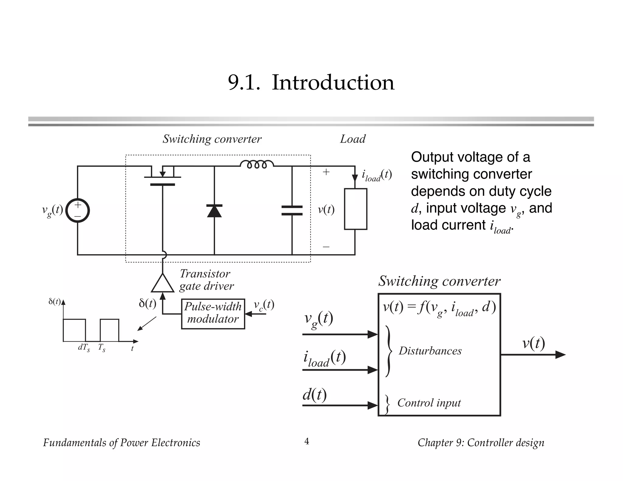
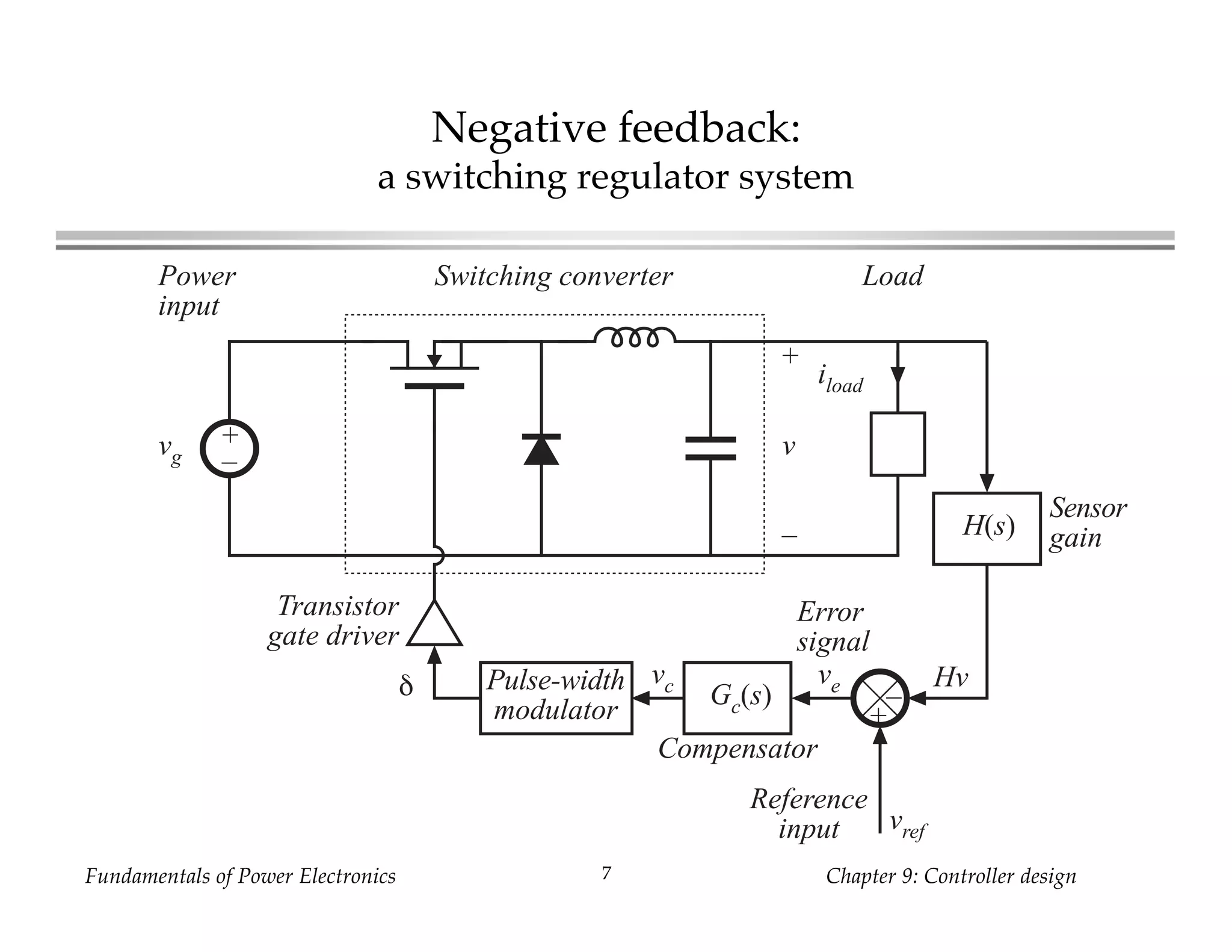
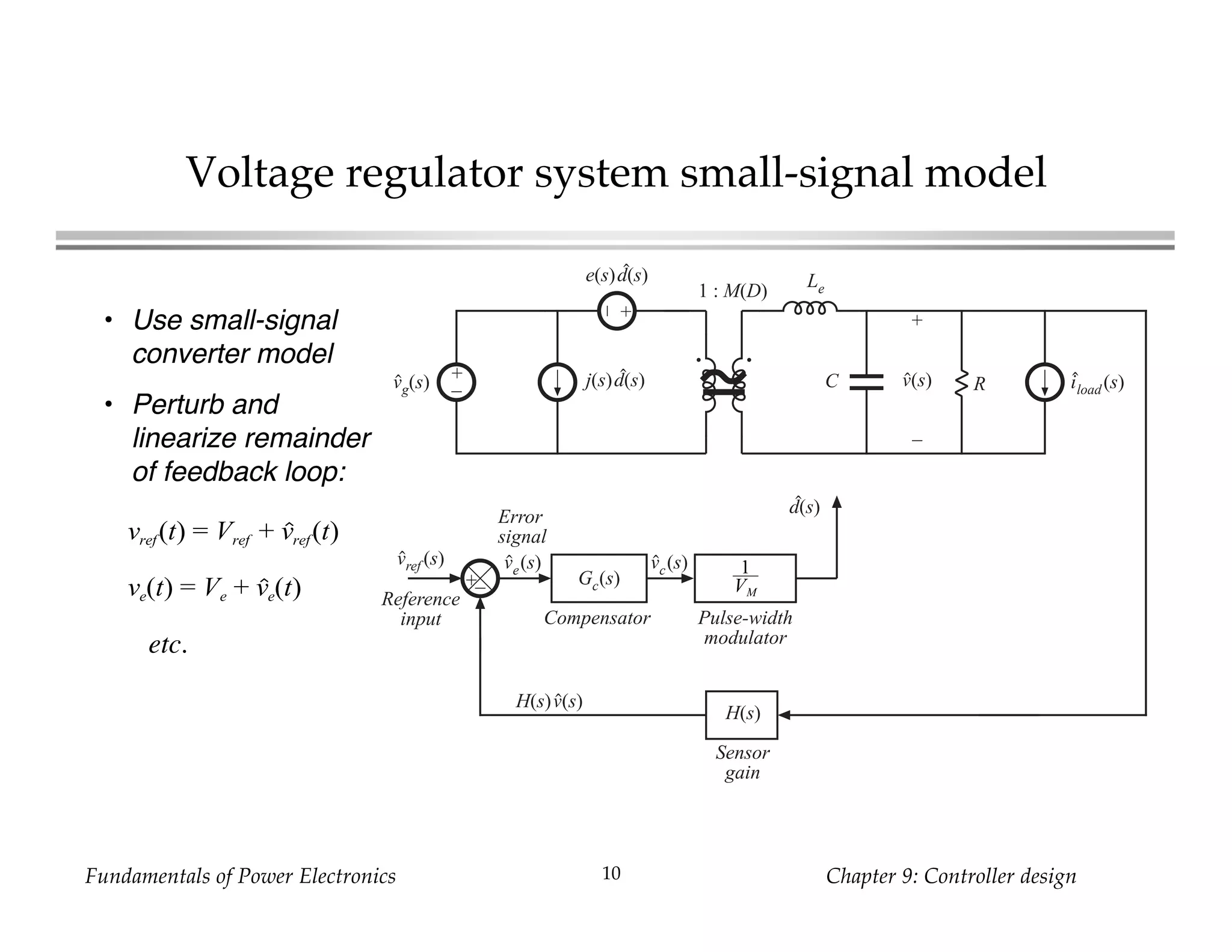
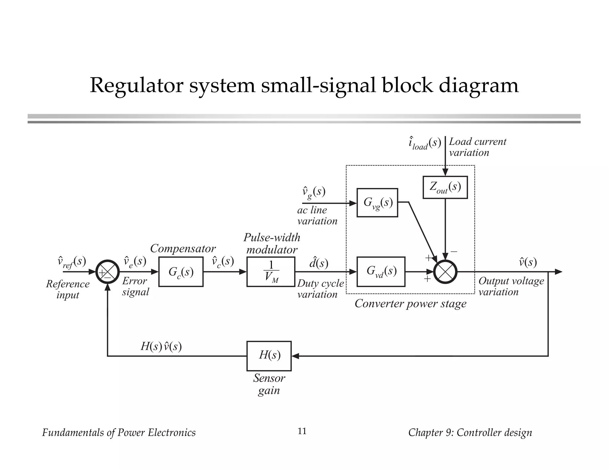
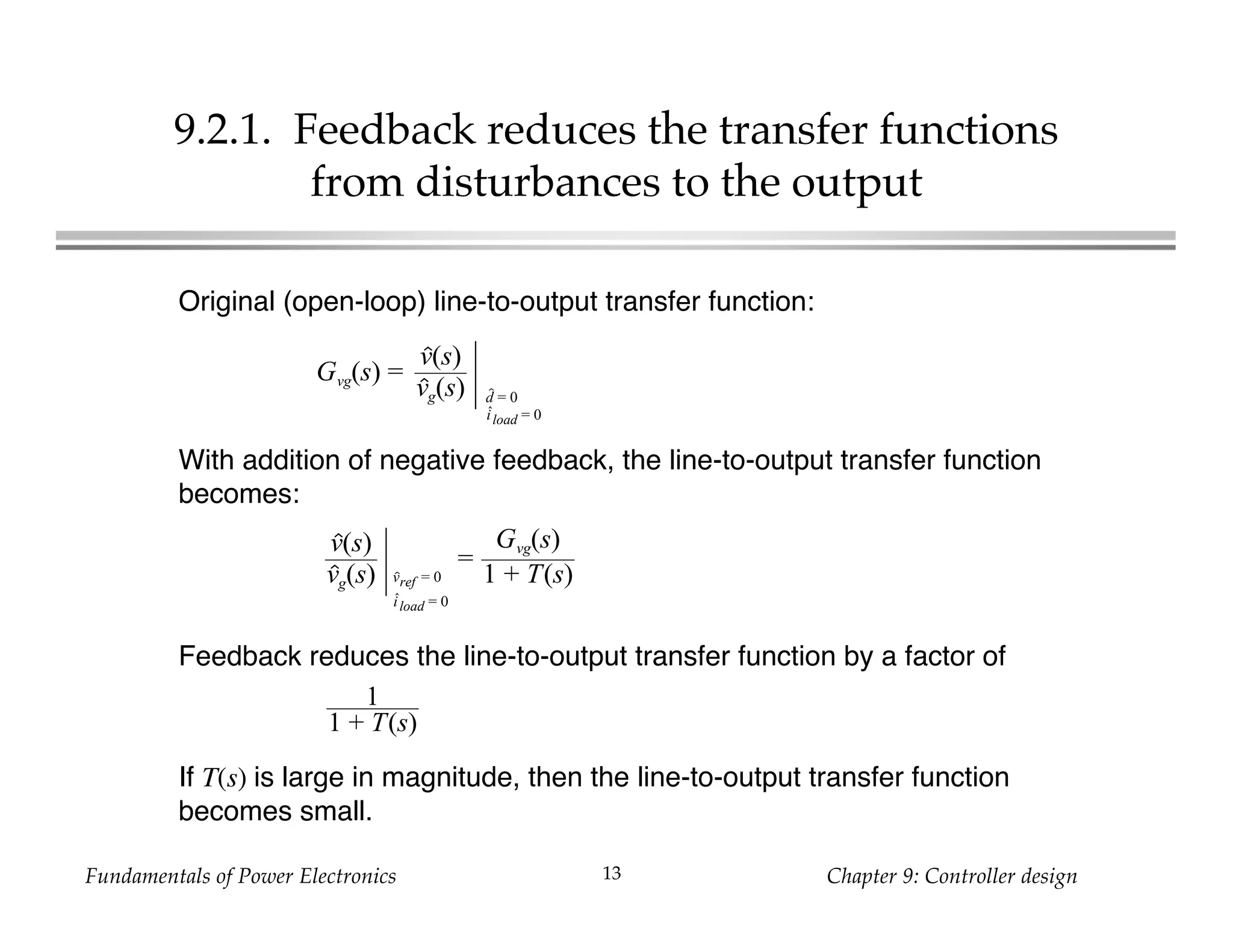
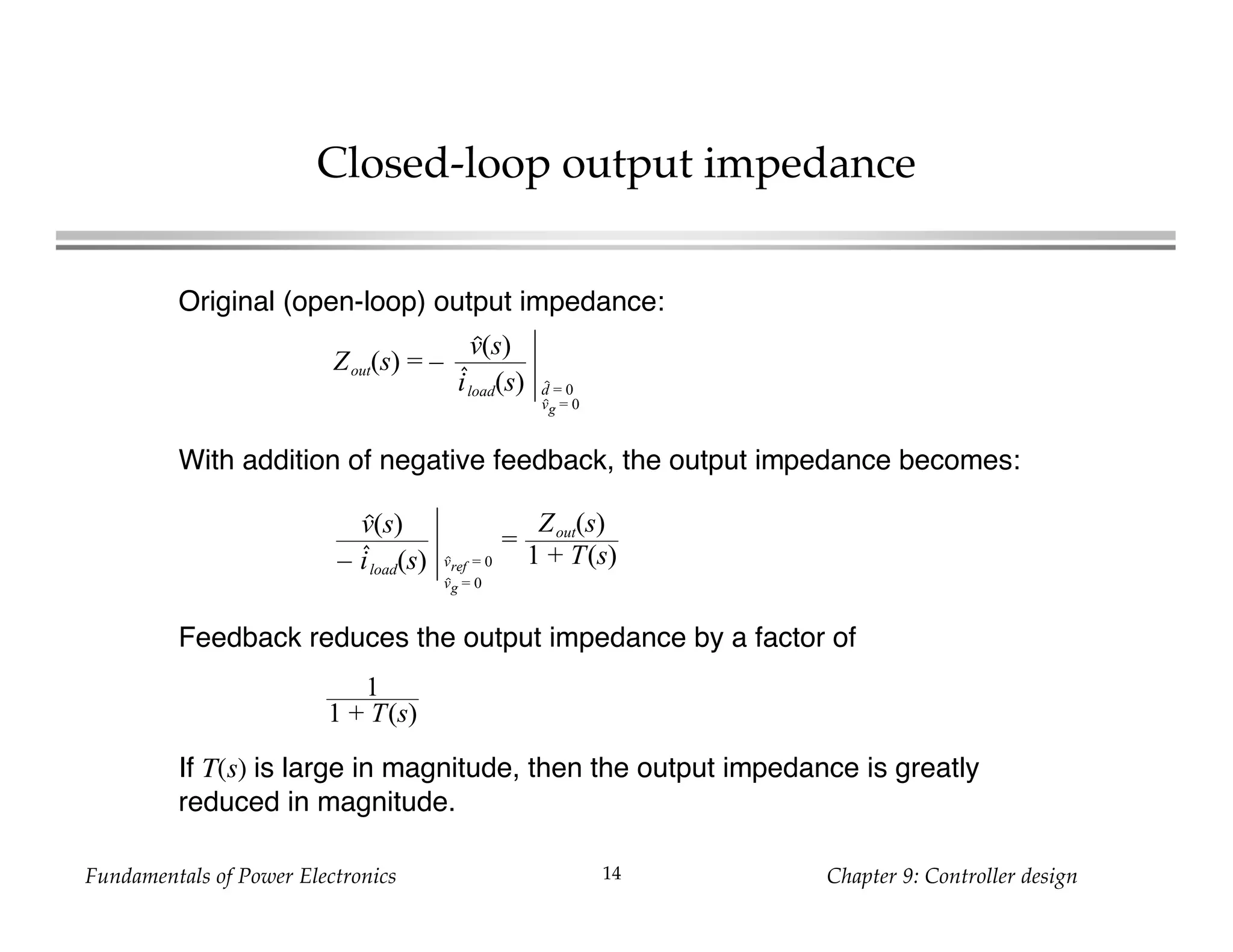
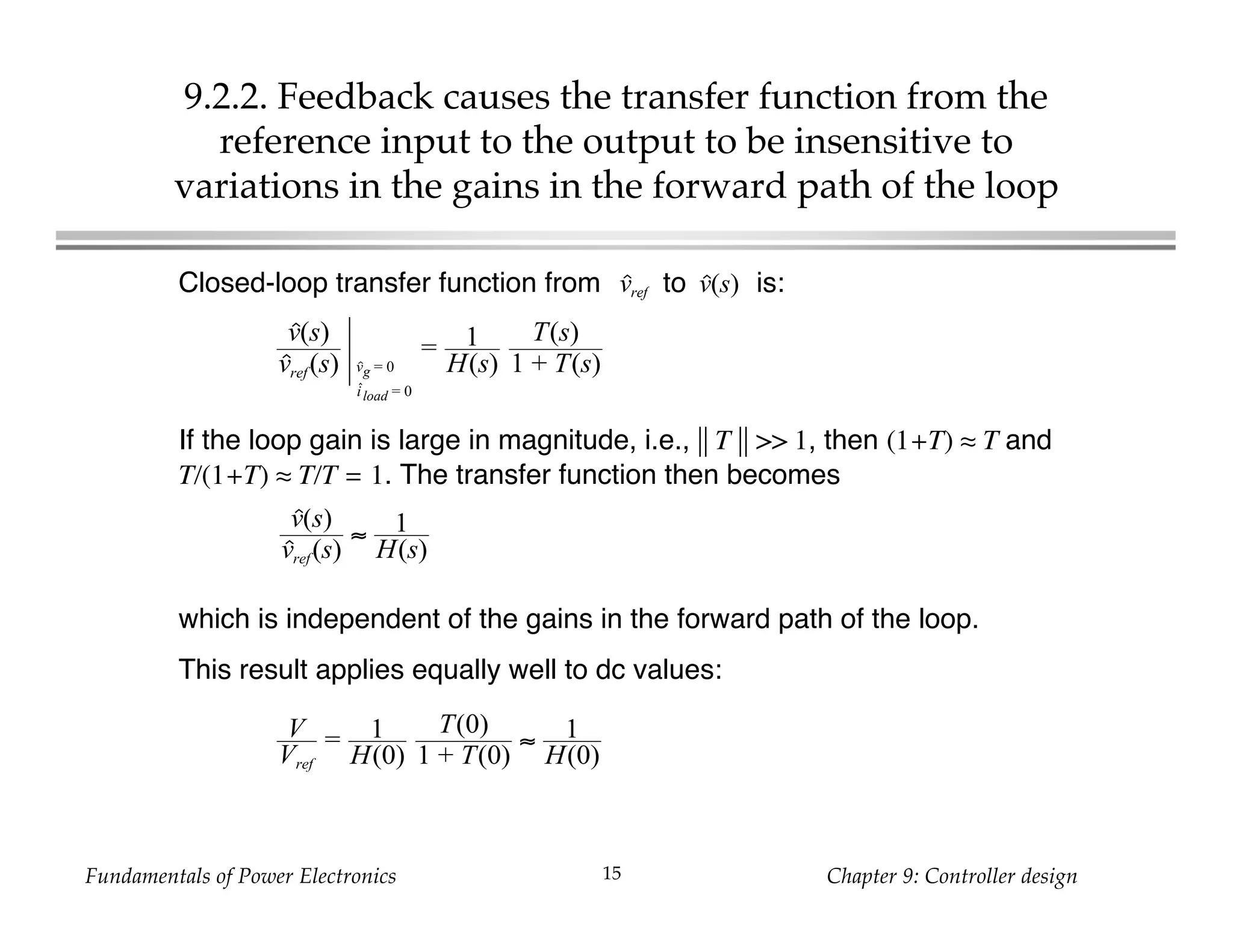
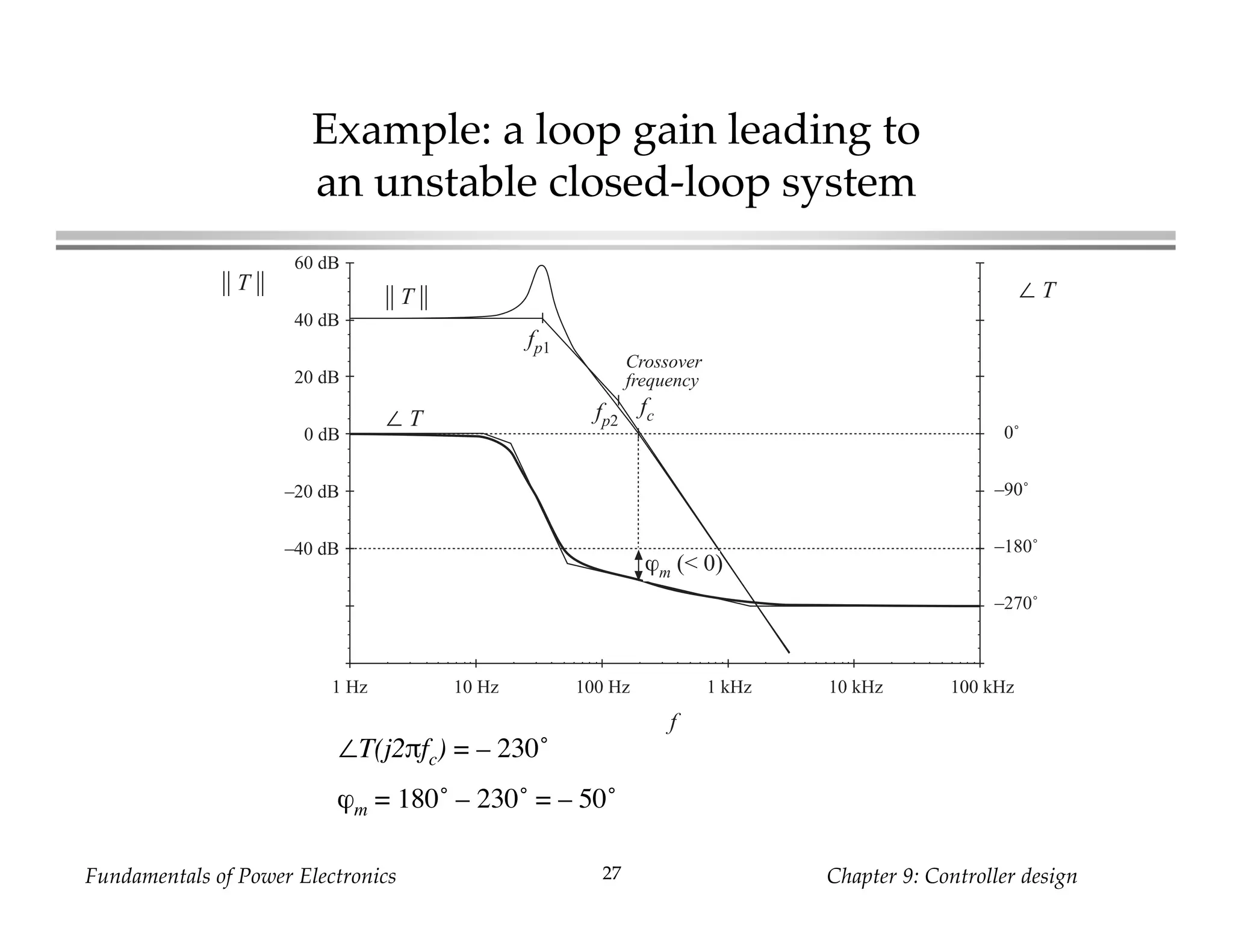
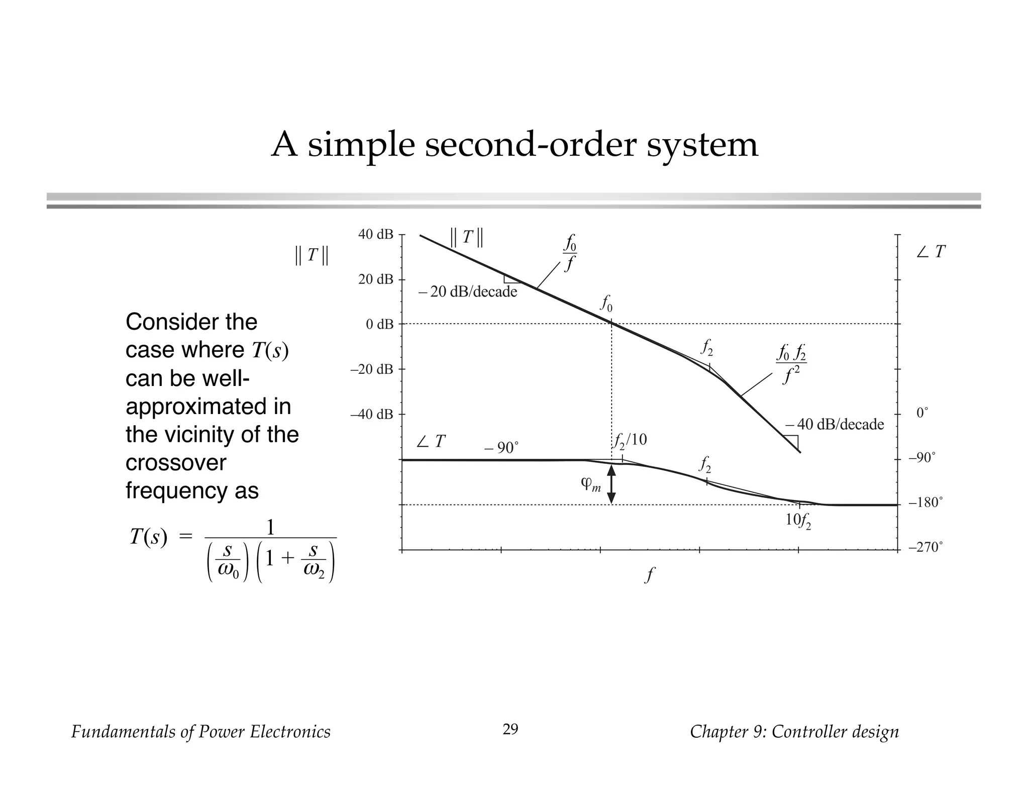
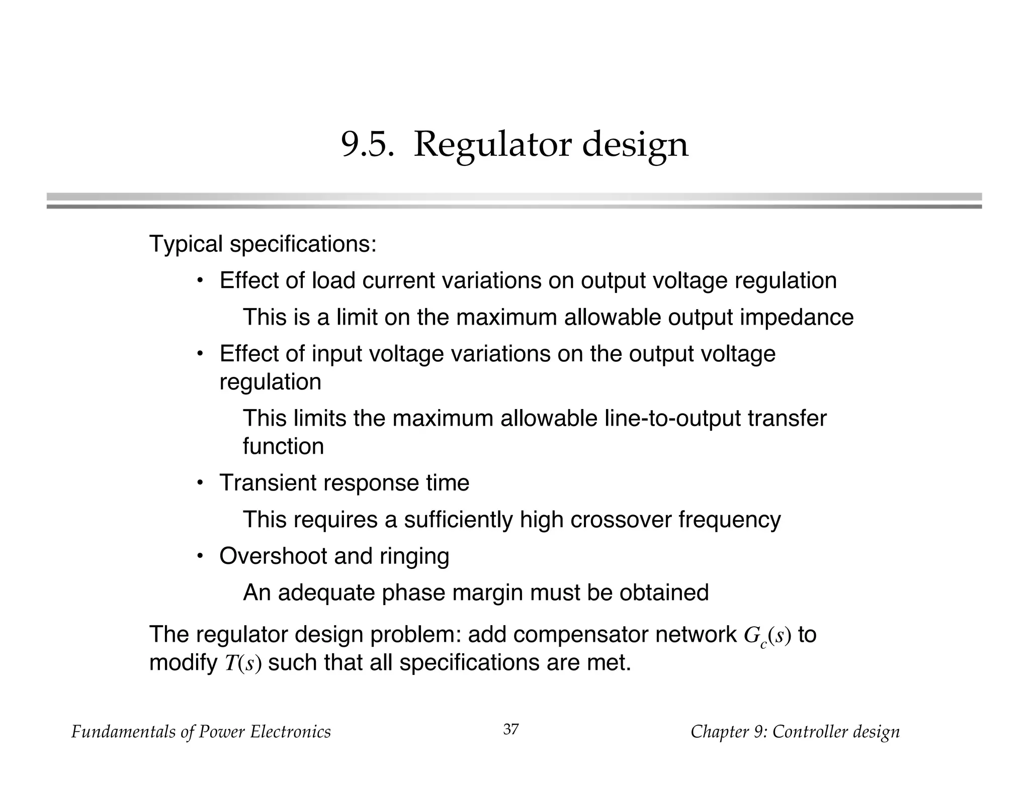
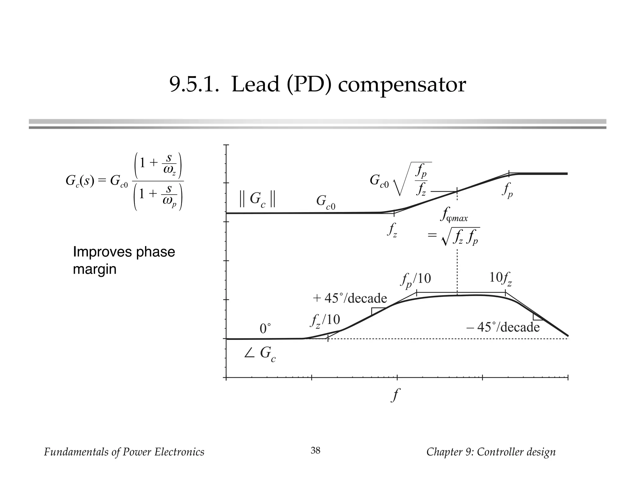
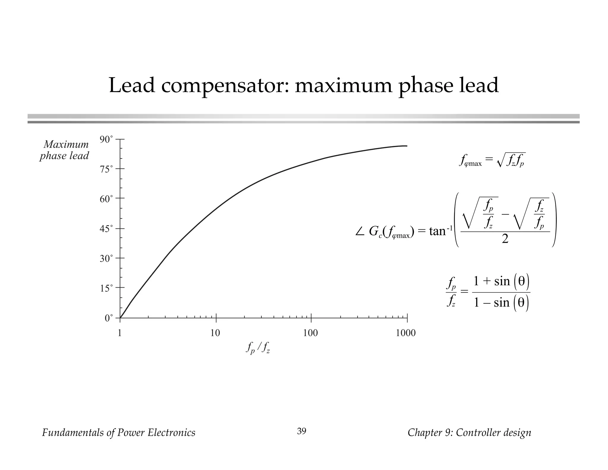
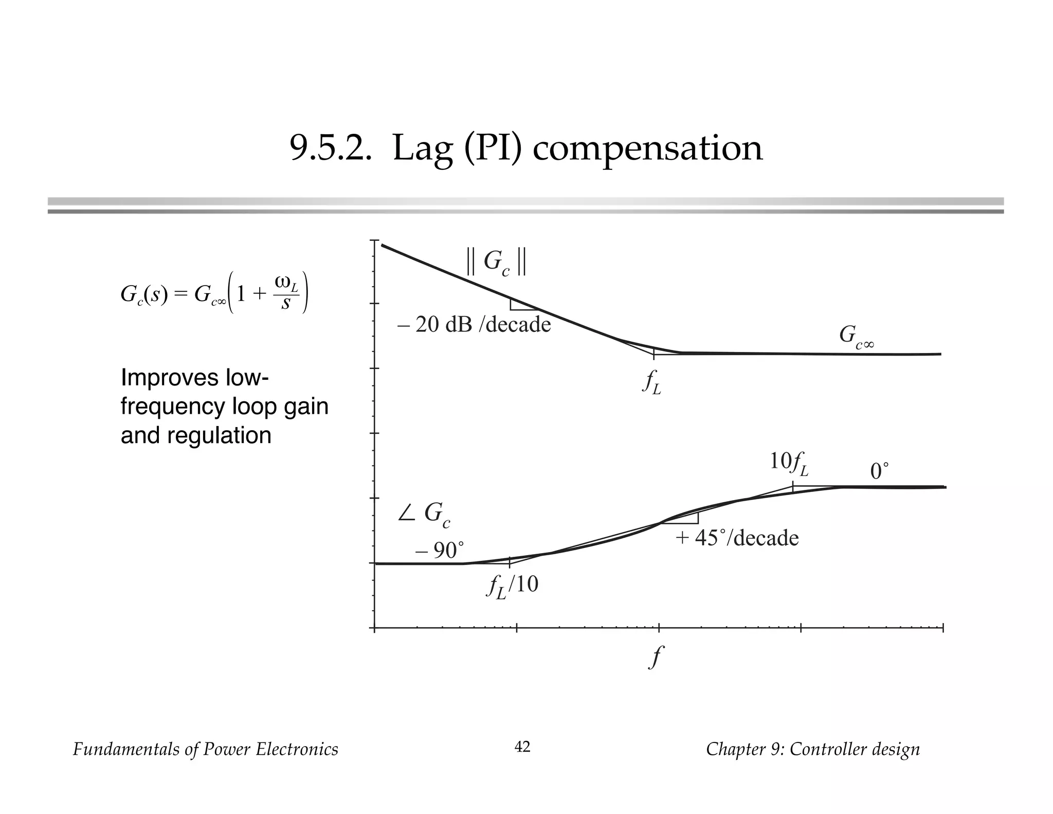
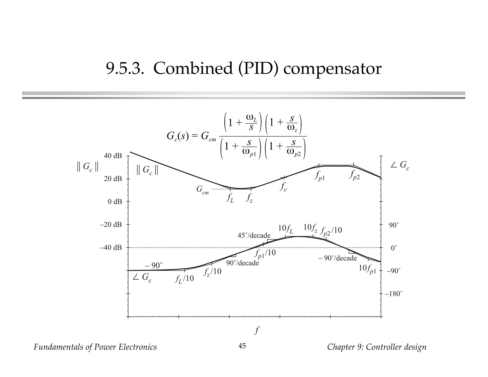
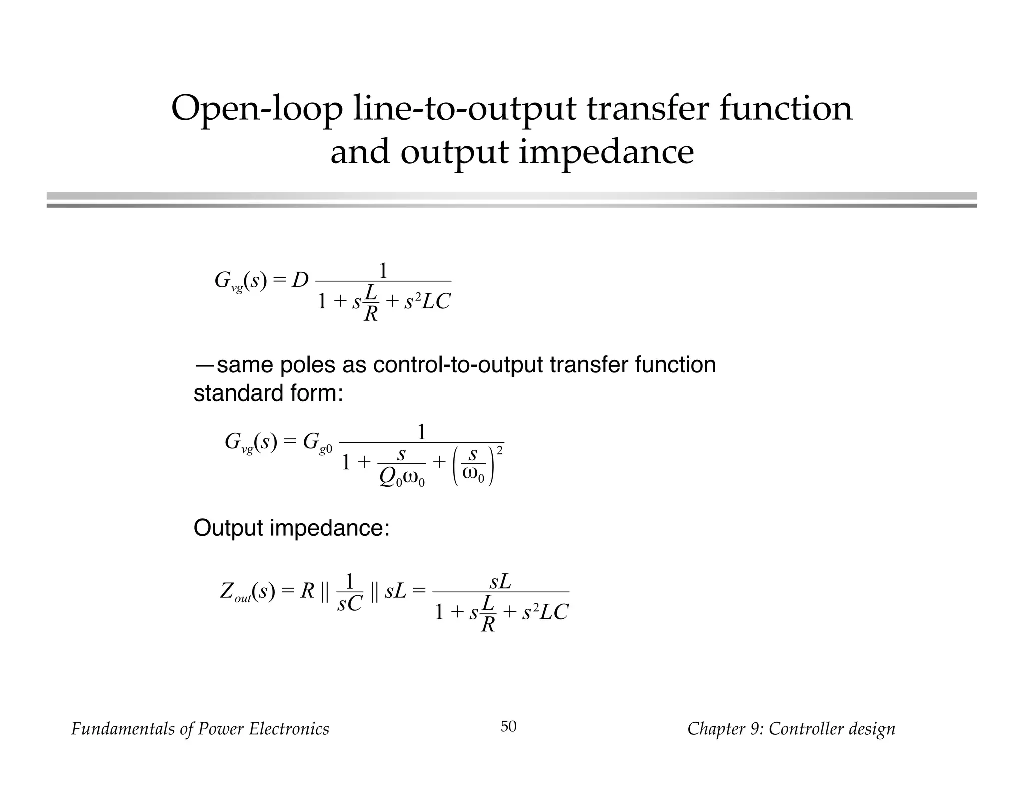
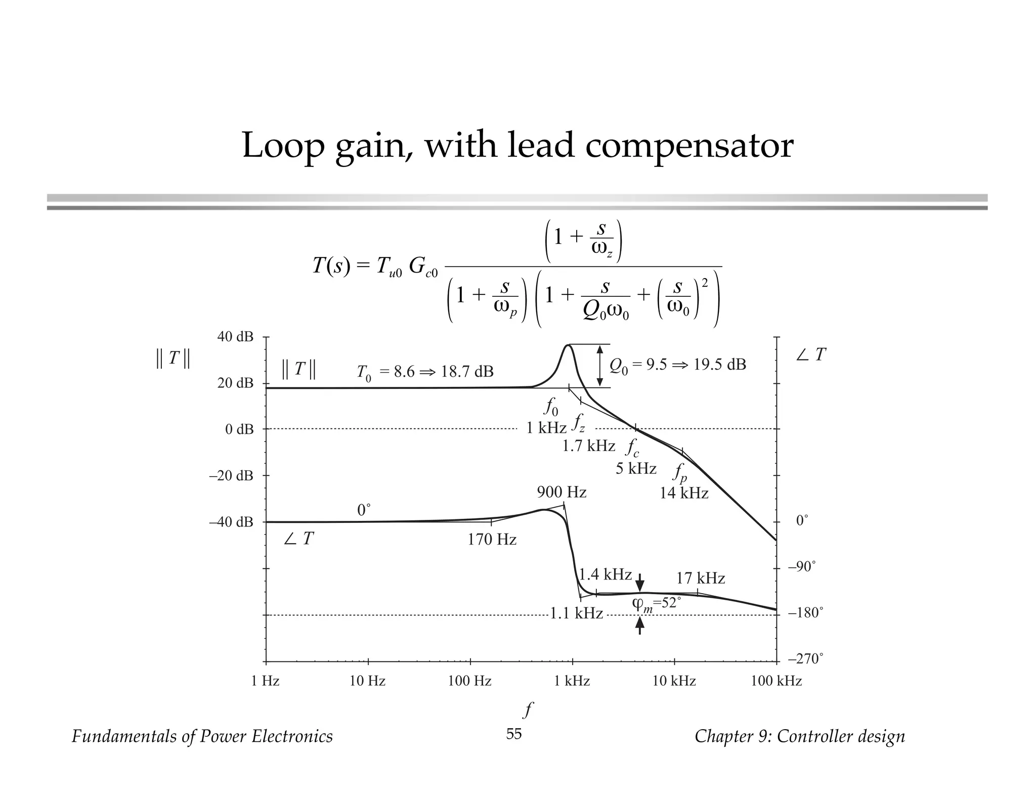
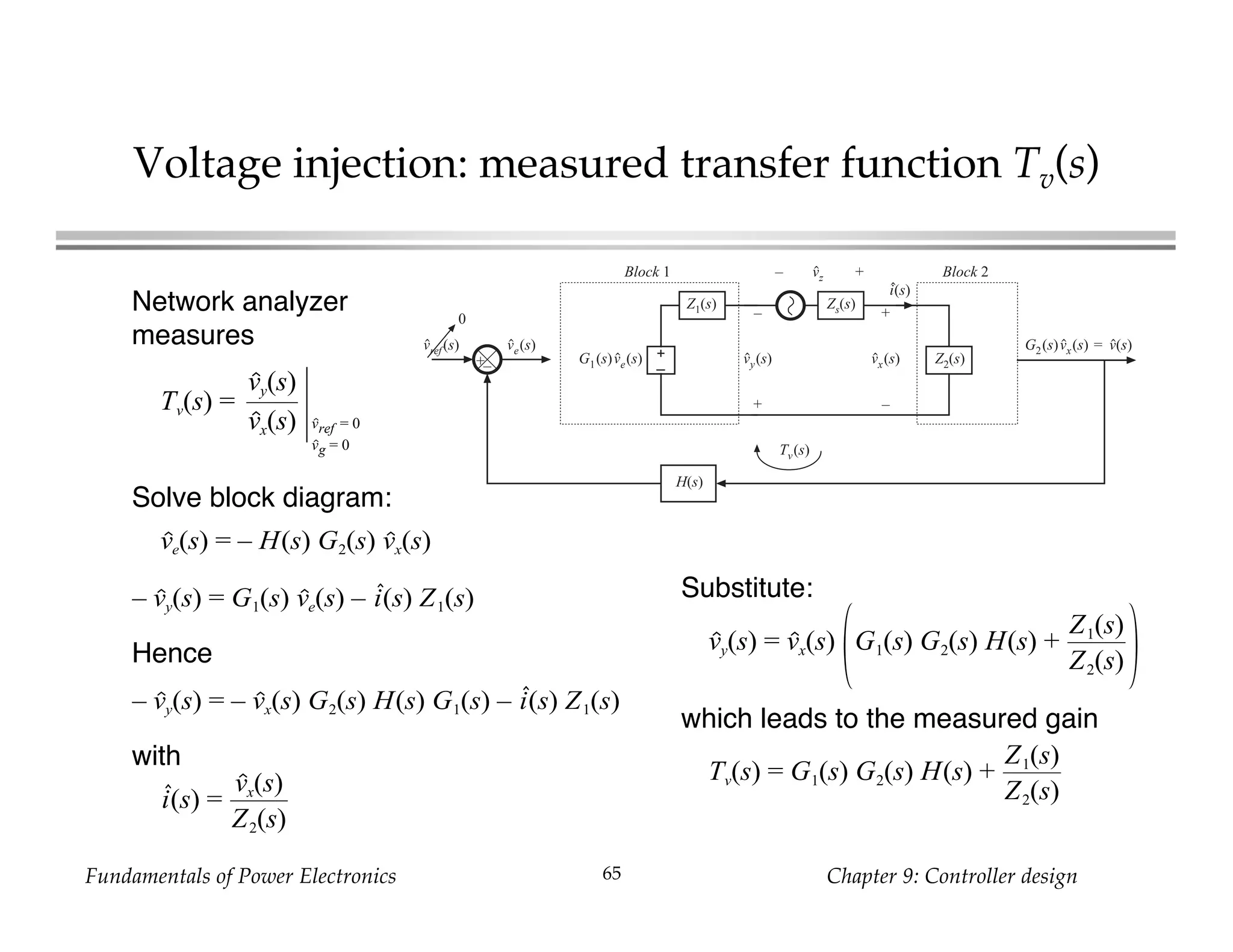
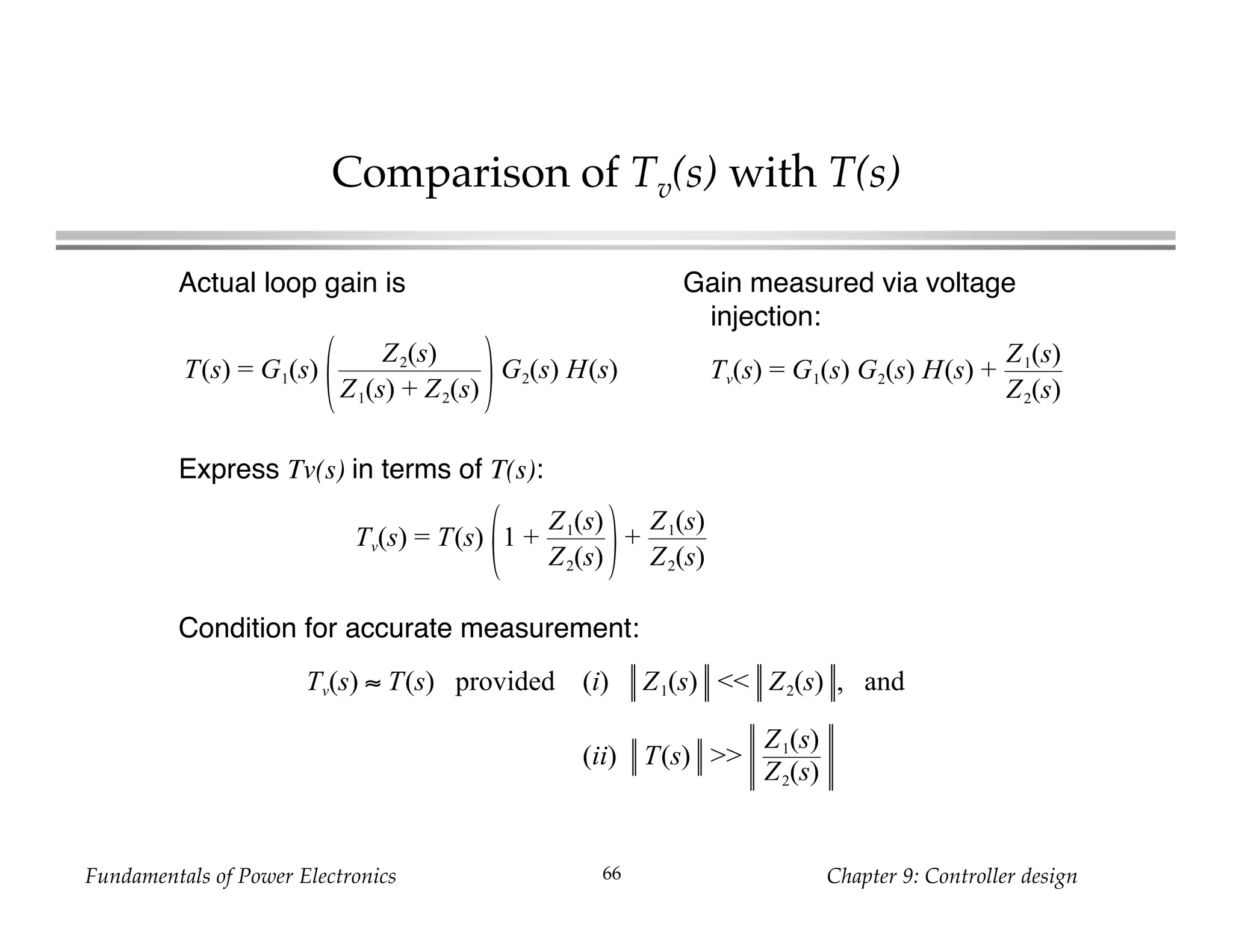
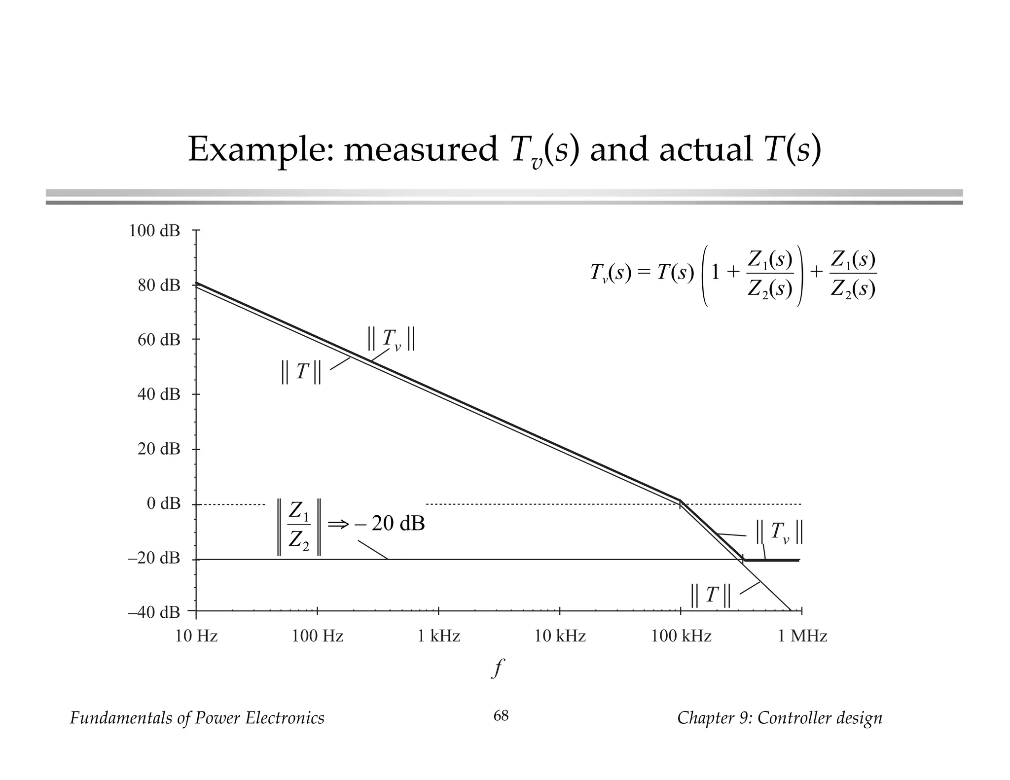
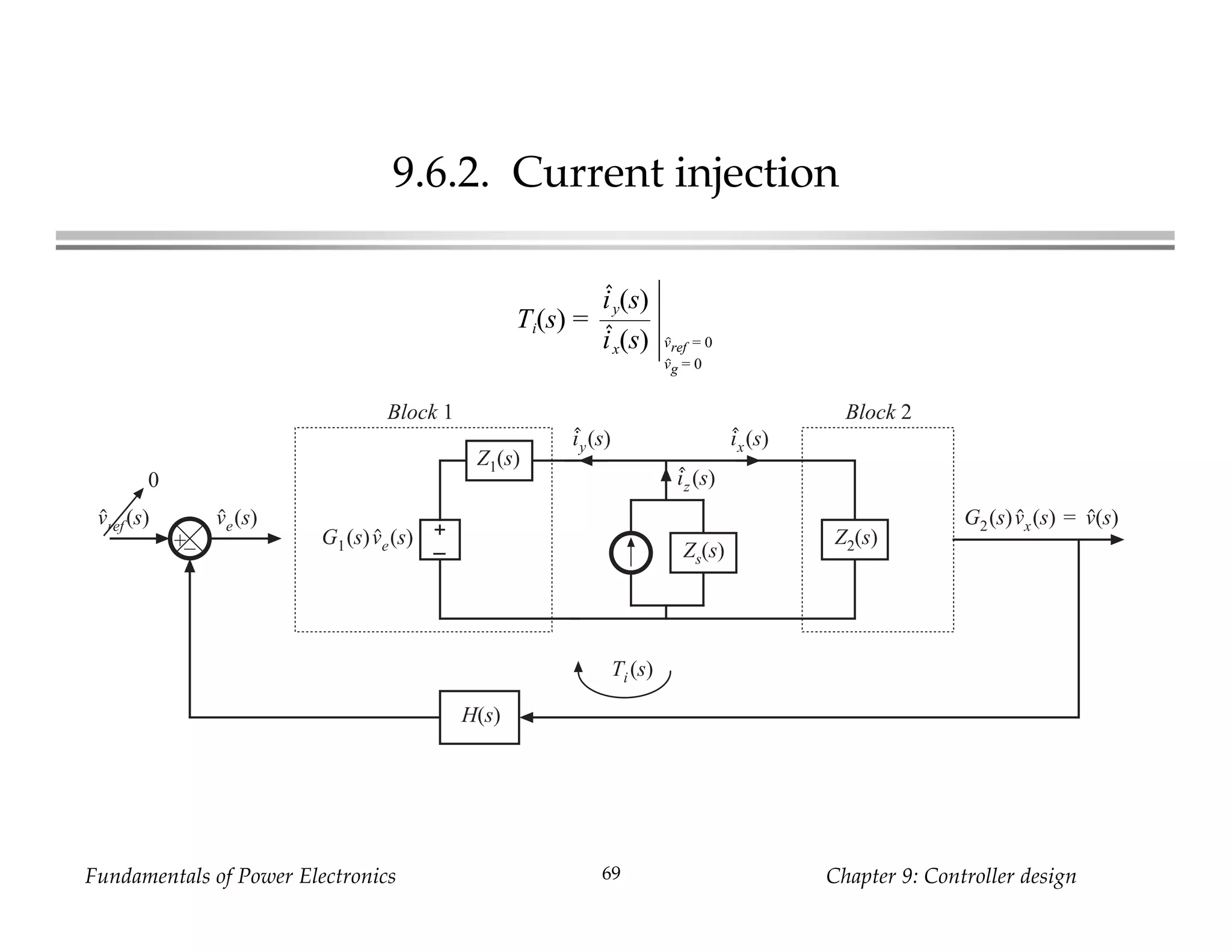
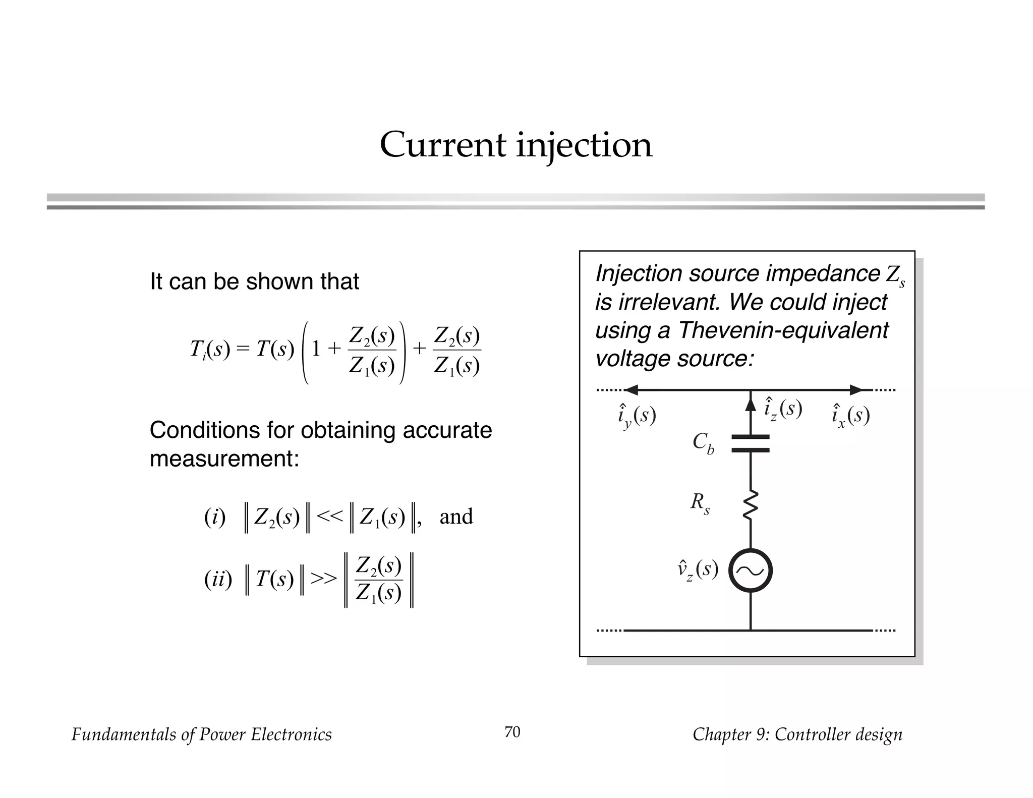
This chapter discusses controller design for power electronics. It begins by introducing negative feedback loops and their effects of reducing disturbances and making the output insensitive to variations in the forward path. Key terms like open-loop, closed-loop, loop gain, and transfer functions are defined. Stability is then analyzed using the phase margin test, which evaluates the phase of the loop gain at the crossover frequency to determine if the closed-loop system contains any right half-plane poles. The chapter covers designing compensators to shape the loop gain for stability and performance. It concludes with measuring loop gains using injection techniques.
IC Design of Power Management Circuits (IV)Claudia Sin
by Wing-Hung Ki
Integrated Power Electronics Laboratory
ECE Dept., HKUST
Clear Water Bay, Hong Kong
www.ee.ust.hk/~eeki
International Symposium on Integrated Circuits
Singapore, Dec. 14, 2009
IC Design of Power Management Circuits (IV)Claudia Sin
by Wing-Hung Ki
Integrated Power Electronics Laboratory
ECE Dept., HKUST
Clear Water Bay, Hong Kong
www.ee.ust.hk/~eeki
International Symposium on Integrated Circuits
Singapore, Dec. 14, 2009
This presentation explains about the introduction of Nyquist Stability criterion. It clearly shows advantages and disadvantages of Nyquist Stability criterion and also explains importance of Nyquist Stability criterion and steps required to sketch the Nyquist plot. It explains about the steps required to sketch Nyquist plot clearly. It also explains about sketching Nyquist plot and determines the stability by using Nyquist Stability criterion with an example.
An alternator is an electrical generator that converts mechanical energy to electrical energy in the form of alternating current. For reasons of cost and simplicity, most alternators use a rotating magnetic field with a stationary armature.
This presentation explains about the introduction of Polar Plot, advantages and disadvantages of polar plot and also steps to draw polar plot. and also explains about how to draw polar plot with an examples. It also explains how to draw polar plot with numerous examples and stability analysis by using polar plot.
Overlap Add, Overlap Save(digital signal processing)Gourab Ghosh
In DSP to solve a convolution of a long duration sequence there are two popular methods. Overlap Add, Overlap Save. In this presentation i've discussed about both.
- Gourab Ghosh
Analysis and Comparison of CMOS Comparator At 90 NM TechnologyIJERA Editor
In this paper, A CMOS comparator with low power dissipation is presented. The preamplifier latch comparator is compared with conventional double tail comparator. The comparators designed and simulated in 90nm Cadence virtuoso environment technology. The particular preamplifier latch comparator will be mix of a good amplifier and a latch comparator can easily effect higher velocity and also low electric power dissipation. The proposed circuit topology improves kickback noise and reduces power dissipation compared with a conventional double tail comparator.Analysis are testified and compared with conventional comparator and enhancements are detected in this paper.
Accelerate your Kubernetes clusters with Varnish CachingThijs Feryn
A presentation about the usage and availability of Varnish on Kubernetes. This talk explores the capabilities of Varnish caching and shows how to use the Varnish Helm chart to deploy it to Kubernetes.
This presentation was delivered at K8SUG Singapore. See https://feryn.eu/presentations/accelerate-your-kubernetes-clusters-with-varnish-caching-k8sug-singapore-28-2024 for more details.
UiPath Test Automation using UiPath Test Suite series, part 3DianaGray10
Welcome to UiPath Test Automation using UiPath Test Suite series part 3. In this session, we will cover desktop automation along with UI automation.
Topics covered:
UI automation Introduction,
UI automation Sample
Desktop automation flow
Pradeep Chinnala, Senior Consultant Automation Developer @WonderBotz and UiPath MVP
Deepak Rai, Automation Practice Lead, Boundaryless Group and UiPath MVP
Connector Corner: Automate dynamic content and events by pushing a buttonDianaGray10
Here is something new! In our next Connector Corner webinar, we will demonstrate how you can use a single workflow to:
Create a campaign using Mailchimp with merge tags/fields
Send an interactive Slack channel message (using buttons)
Have the message received by managers and peers along with a test email for review
But there’s more:
In a second workflow supporting the same use case, you’ll see:
Your campaign sent to target colleagues for approval
If the “Approve” button is clicked, a Jira/Zendesk ticket is created for the marketing design team
But—if the “Reject” button is pushed, colleagues will be alerted via Slack message
Join us to learn more about this new, human-in-the-loop capability, brought to you by Integration Service connectors.
And...
Speakers:
Akshay Agnihotri, Product Manager
Charlie Greenberg, Host
JMeter webinar - integration with InfluxDB and GrafanaRTTS
Watch this recorded webinar about real-time monitoring of application performance. See how to integrate Apache JMeter, the open-source leader in performance testing, with InfluxDB, the open-source time-series database, and Grafana, the open-source analytics and visualization application.
In this webinar, we will review the benefits of leveraging InfluxDB and Grafana when executing load tests and demonstrate how these tools are used to visualize performance metrics.
Length: 30 minutes
Session Overview
-------------------------------------------
During this webinar, we will cover the following topics while demonstrating the integrations of JMeter, InfluxDB and Grafana:
- What out-of-the-box solutions are available for real-time monitoring JMeter tests?
- What are the benefits of integrating InfluxDB and Grafana into the load testing stack?
- Which features are provided by Grafana?
- Demonstration of InfluxDB and Grafana using a practice web application
To view the webinar recording, go to:
https://www.rttsweb.com/jmeter-integration-webinar
UiPath Test Automation using UiPath Test Suite series, part 4DianaGray10
Welcome to UiPath Test Automation using UiPath Test Suite series part 4. In this session, we will cover Test Manager overview along with SAP heatmap.
The UiPath Test Manager overview with SAP heatmap webinar offers a concise yet comprehensive exploration of the role of a Test Manager within SAP environments, coupled with the utilization of heatmaps for effective testing strategies.
Participants will gain insights into the responsibilities, challenges, and best practices associated with test management in SAP projects. Additionally, the webinar delves into the significance of heatmaps as a visual aid for identifying testing priorities, areas of risk, and resource allocation within SAP landscapes. Through this session, attendees can expect to enhance their understanding of test management principles while learning practical approaches to optimize testing processes in SAP environments using heatmap visualization techniques
What will you get from this session?
1. Insights into SAP testing best practices
2. Heatmap utilization for testing
3. Optimization of testing processes
4. Demo
Topics covered:
Execution from the test manager
Orchestrator execution result
Defect reporting
SAP heatmap example with demo
Speaker:
Deepak Rai, Automation Practice Lead, Boundaryless Group and UiPath MVP
The Art of the Pitch: WordPress Relationships and SalesLaura Byrne
Clients don’t know what they don’t know. What web solutions are right for them? How does WordPress come into the picture? How do you make sure you understand scope and timeline? What do you do if sometime changes?
All these questions and more will be explored as we talk about matching clients’ needs with what your agency offers without pulling teeth or pulling your hair out. Practical tips, and strategies for successful relationship building that leads to closing the deal.
GDG Cloud Southlake #33: Boule & Rebala: Effective AppSec in SDLC using Deplo...James Anderson
Effective Application Security in Software Delivery lifecycle using Deployment Firewall and DBOM
The modern software delivery process (or the CI/CD process) includes many tools, distributed teams, open-source code, and cloud platforms. Constant focus on speed to release software to market, along with the traditional slow and manual security checks has caused gaps in continuous security as an important piece in the software supply chain. Today organizations feel more susceptible to external and internal cyber threats due to the vast attack surface in their applications supply chain and the lack of end-to-end governance and risk management.
The software team must secure its software delivery process to avoid vulnerability and security breaches. This needs to be achieved with existing tool chains and without extensive rework of the delivery processes. This talk will present strategies and techniques for providing visibility into the true risk of the existing vulnerabilities, preventing the introduction of security issues in the software, resolving vulnerabilities in production environments quickly, and capturing the deployment bill of materials (DBOM).
Speakers:
Bob Boule
Robert Boule is a technology enthusiast with PASSION for technology and making things work along with a knack for helping others understand how things work. He comes with around 20 years of solution engineering experience in application security, software continuous delivery, and SaaS platforms. He is known for his dynamic presentations in CI/CD and application security integrated in software delivery lifecycle.
Gopinath Rebala
Gopinath Rebala is the CTO of OpsMx, where he has overall responsibility for the machine learning and data processing architectures for Secure Software Delivery. Gopi also has a strong connection with our customers, leading design and architecture for strategic implementations. Gopi is a frequent speaker and well-known leader in continuous delivery and integrating security into software delivery.
State of ICS and IoT Cyber Threat Landscape Report 2024 previewPrayukth K V
The IoT and OT threat landscape report has been prepared by the Threat Research Team at Sectrio using data from Sectrio, cyber threat intelligence farming facilities spread across over 85 cities around the world. In addition, Sectrio also runs AI-based advanced threat and payload engagement facilities that serve as sinks to attract and engage sophisticated threat actors, and newer malware including new variants and latent threats that are at an earlier stage of development.
The latest edition of the OT/ICS and IoT security Threat Landscape Report 2024 also covers:
State of global ICS asset and network exposure
Sectoral targets and attacks as well as the cost of ransom
Global APT activity, AI usage, actor and tactic profiles, and implications
Rise in volumes of AI-powered cyberattacks
Major cyber events in 2024
Malware and malicious payload trends
Cyberattack types and targets
Vulnerability exploit attempts on CVEs
Attacks on counties – USA
Expansion of bot farms – how, where, and why
In-depth analysis of the cyber threat landscape across North America, South America, Europe, APAC, and the Middle East
Why are attacks on smart factories rising?
Cyber risk predictions
Axis of attacks – Europe
Systemic attacks in the Middle East
Download the full report from here:
https://sectrio.com/resources/ot-threat-landscape-reports/sectrio-releases-ot-ics-and-iot-security-threat-landscape-report-2024/
Smart TV Buyer Insights Survey 2024 by 91mobiles.pdf91mobiles
91mobiles recently conducted a Smart TV Buyer Insights Survey in which we asked over 3,000 respondents about the TV they own, aspects they look at on a new TV, and their TV buying preferences.
GraphRAG is All You need? LLM & Knowledge GraphGuy Korland
Guy Korland, CEO and Co-founder of FalkorDB, will review two articles on the integration of language models with knowledge graphs.
1. Unifying Large Language Models and Knowledge Graphs: A Roadmap.
https://arxiv.org/abs/2306.08302
2. Microsoft Research's GraphRAG paper and a review paper on various uses of knowledge graphs:
https://www.microsoft.com/en-us/research/blog/graphrag-unlocking-llm-discovery-on-narrative-private-data/
1. Fundamentals of Power Electronics Chapter 9: Controller design1
Chapter 9. Controller Design
9.1. Introduction
9.2. Effect of negative feedback on the network transfer
functions
9.2.1. Feedback reduces the transfer function from disturbances
to the output
9.2.2. Feedback causes the transfer function from the reference
input to the output to be insensitive to variations in the gains
in the forward path of the loop
9.3. Construction of the important quantities 1/(1+T) and
T/(1+T) and the closed-loop transfer functions
2. Fundamentals of Power Electronics Chapter 9: Controller design2
Controller design
9.4. Stability
9.4.1. The phase margin test
9.4.2. The relation between phase margin and closed-loop
damping factor
9.4.3. Transient response vs. damping factor
9.5. Regulator design
9.5.1. Lead (PD) compensator
9.5.2. Lag (PI) compensator
9.5.3. Combined (PID) compensator
9.5.4. Design example
3. Fundamentals of Power Electronics Chapter 9: Controller design3
Controller design
9.6. Measurement of loop gains
9.6.1. Voltage injection
9.6.2. Current injection
9.6.3. Measurement of unstable systems
9.7. Summary of key points
4. Fundamentals of Power Electronics Chapter 9: Controller design4
9.1. Introduction
Output voltage of a
switching converter
depends on duty cycle
d, input voltage vg, and
load current iload.
+
–
+
v(t)
–
vg(t)
Switching converter Load
Pulse-width
modulator
vc(t)
Transistor
gate driver
δ(t)
iload(t)
δ(t)
TsdTs t v(t)
vg(t)
iload(t)
d(t)
Switching converter
Disturbances
Control input
}
}
v(t) = f(vg, iload, d)
5. Fundamentals of Power Electronics Chapter 9: Controller design5
The dc regulator application
Objective: maintain constant
output voltage v(t) = V, in spite
of disturbances in vg(t) and
iload(t).
Typical variation in vg(t): 100Hz
or 120Hz ripple, produced by
rectifier circuit.
Load current variations: a significant step-change in load current, such
as from 50% to 100% of rated value, may be applied.
A typical output voltage regulation specification: 5V ± 0.1V.
Circuit elements are constructed to some specified tolerance. In high
volume manufacturing of converters, all output voltages must meet
specifications.
v(t)
vg(t)
iload(t)
d(t)
Switching converter
Disturbances
Control input
}
}
v(t) = f(vg
, iload
, d)
6. Fundamentals of Power Electronics Chapter 9: Controller design6
The dc regulator application
So we cannot expect to set the duty cycle to a single value, and obtain
a given constant output voltage under all conditions.
Negative feedback: build a circuit that automatically adjusts the duty
cycle as necessary, to obtain the specified output voltage with high
accuracy, regardless of disturbances or component tolerances.
7. Fundamentals of Power Electronics Chapter 9: Controller design7
Negative feedback:
a switching regulator system
+
–
+
v
–
vg
Switching converterPower
input
Load
–+
Compensator
vref
Reference
input
HvPulse-width
modulator
vc
Transistor
gate driver
δ Gc(s)
H(s)
ve
Error
signal
Sensor
gain
iload
8. Fundamentals of Power Electronics Chapter 9: Controller design8
Negative feedback
vref
Reference
input
vcve(t)
Error
signal
Sensor
gain
v(t)
vg(t)
iload(t)
d(t)
Switching converter
Disturbances
Control input
}
}+– Pulse-width
modulator
Compensator
v(t) = f(vg, iload, d)
9. Fundamentals of Power Electronics Chapter 9: Controller design9
9.2. Effect of negative feedback on the
network transfer functions
Small signal model: open-loop converter
Output voltage can be expressed as
where
v(s) = Gvd(s) d(s) + Gvg(s) vg(s) – Zout(s) iload(s)
Gvd(s) =
v(s)
d(s) vg = 0
iload = 0
Gvg(s) =
v(s)
vg(s) d = 0
iload = 0
Zout(s) = –
v(s)
iload(s) d = 0
vg = 0
+
–
+
– 1 : M(D)
Le
C Rvg(s) j(s)d(s)
e(s)d(s)
iload(s)
+
v(s)
–
10. Fundamentals of Power Electronics Chapter 9: Controller design10
Voltage regulator system small-signal model
• Use small-signal
converter model
• Perturb and
linearize remainder
of feedback loop:
vref(t) = Vref + vref(t)
ve(t) = Ve + ve(t)
etc.
Reference
input
Error
signal
+
–
Pulse-width
modulator
Compensator
Gc(s)
Sensor
gain
H(s)
1
VM
+
–
+
–
1 : M(D)
Le
C Rvg(s) j(s)d(s)
e(s)d(s)
iload(s)
+
v(s)
–
d(s)
vref (s)
H(s)v(s)
ve(s) vc(s)
11. Fundamentals of Power Electronics Chapter 9: Controller design11
Regulator system small-signal block diagram
Reference
input
Error
signal
+
–
Pulse-width
modulatorCompensator
Sensor
gain
H(s)
1
VM
Duty cycle
variation
Gc(s) Gvd(s)
Gvg(s)
Zout(s)
ac line
variation
Load current
variation
+
–
+
Output voltage
variation
Converter power stage
vref(s) ve(s) vc(s) d(s)
vg(s)
iload(s)
v(s)
H(s)v(s)
12. Fundamentals of Power Electronics Chapter 9: Controller design12
Solution of block diagram
v = vref
GcGvd / VM
1 + HGcGvd / VM
+ vg
Gvg
1 + HGcGvd / VM
– iload
Zout
1 + HGcGvd / VM
Manipulate block diagram to solve for . Result isv(s)
which is of the form
v = vref
1
H
T
1 + T
+ vg
Gvg
1 + T
– iload
Zout
1 + T
with T(s) = H(s) Gc(s) Gvd(s) / VM = "loop gain"
Loop gain T(s) = products of the gains around the negative
feedback loop.
13. Fundamentals of Power Electronics Chapter 9: Controller design13
9.2.1. Feedback reduces the transfer functions
from disturbances to the output
Original (open-loop) line-to-output transfer function:
Gvg(s) =
v(s)
vg(s) d = 0
iload = 0
With addition of negative feedback, the line-to-output transfer function
becomes:
v(s)
vg(s) vref = 0
iload = 0
=
Gvg(s)
1 + T(s)
Feedback reduces the line-to-output transfer function by a factor of
1
1 + T(s)
If T(s) is large in magnitude, then the line-to-output transfer function
becomes small.
14. Fundamentals of Power Electronics Chapter 9: Controller design14
Closed-loop output impedance
Original (open-loop) output impedance:
With addition of negative feedback, the output impedance becomes:
Feedback reduces the output impedance by a factor of
1
1 + T(s)
If T(s) is large in magnitude, then the output impedance is greatly
reduced in magnitude.
Zout(s) = –
v(s)
iload(s) d = 0
vg = 0
v(s)
– iload(s) vref = 0
vg = 0
=
Zout(s)
1 + T(s)
15. Fundamentals of Power Electronics Chapter 9: Controller design15
9.2.2. Feedback causes the transfer function from the
reference input to the output to be insensitive to
variations in the gains in the forward path of the loop
Closed-loop transfer function from to is:
which is independent of the gains in the forward path of the loop.
This result applies equally well to dc values:
v(s)vref
v(s)
vref(s) vg = 0
iload = 0
= 1
H(s)
T(s)
1 + T(s)
If the loop gain is large in magnitude, i.e., || T || >> 1, then (1+T) ≈ T and
T/(1+T) ≈ T/T = 1. The transfer function then becomes
v(s)
vref(s)
≈ 1
H(s)
V
Vref
= 1
H(0)
T(0)
1 + T(0)
≈ 1
H(0)
16. Fundamentals of Power Electronics Chapter 9: Controller design16
9.3. Construction of the important quantities
1/(1+T) and T/(1+T)
Example
T(s) = T0
1 + s
ωz
1 + s
Qωp1
+ s
ωp1
2
1 + s
ωp2
At the crossover frequency fc, || T || = 1
fp1
QdB
– 40 dB/decade
| T0 |dB
fz
fc
fp2
– 20 dB/decade
Crossover
frequency
f
|| T ||
0 dB
–20 dB
–40 dB
20 dB
40 dB
60 dB
80 dB
– 40 dB/decade
1 Hz 10 Hz 100 Hz 1 kHz 10 kHz 100 kHz
17. Fundamentals of Power Electronics Chapter 9: Controller design17
Approximating 1/(1+T) and T/(1+T)
T
1 + T
≈
1 for || T || >> 1
T for || T || << 1
1
1+T(s)
≈
1
T(s)
for || T || >> 1
1 for || T || << 1
18. Fundamentals of Power Electronics Chapter 9: Controller design18
Example: construction of T/(1+T)
T
1 + T
≈
1 for || T || >> 1
T for || T || << 1
fp1
fz
fc
fp2
– 20 dB/decade
– 40 dB/decade
Crossover
frequency
f
|| T ||
0 dB
–20 dB
–40 dB
20 dB
40 dB
60 dB
80 dB
T
1 + T
1 Hz 10 Hz 100 Hz 1 kHz 10 kHz 100 kHz
19. Fundamentals of Power Electronics Chapter 9: Controller design19
Example: analytical expressions for approximate
reference to output transfer function
v(s)
vref(s)
= 1
H(s)
T(s)
1 + T(s)
≈ 1
H(s)
v(s)
vref(s)
= 1
H(s)
T(s)
1 + T(s)
≈
T(s)
H(s)
=
Gc(s)Gvd(s)
VM
At frequencies sufficiently less that the crossover frequency, the loop
gain T(s) has large magnitude. The transfer function from the reference
to the output becomes
This is the desired behavior: the output follows the reference
according to the ideal gain 1/H(s). The feedback loop works well at
frequencies where the loop gain T(s) has large magnitude.
At frequencies above the crossover frequency, || T || < 1. The quantity
T/(1+T) then has magnitude approximately equal to 1, and we obtain
This coincides with the open-loop transfer function from the reference
to the output. At frequencies where || T || < 1, the loop has essentially
no effect on the transfer function from the reference to the output.
20. Fundamentals of Power Electronics Chapter 9: Controller design20
Same example: construction of 1/(1+T)
1
1+T(s)
≈
1
T(s)
for || T || >> 1
1 for || T || << 1fp1
QdB
– 40 dB/decade
| T0 |dB
fz
fc
fp2
Crossover
frequency
|| T ||
0 dB
–20 dB
–40 dB
20 dB
40 dB
60 dB
80 dB
–60 dB
–80 dB
f
1 Hz 10 Hz 100 Hz 1 kHz 10 kHz 100 kHz
QdB
– | T0 |dB
fp1
fz
1
1 + T
– 40 dB/decade
+ 40 dB/decade
+ 20 dB/decade
– 20 dB/decade
21. Fundamentals of Power Electronics Chapter 9: Controller design21
Interpretation: how the loop rejects disturbances
Below the crossover frequency: f < fc
and || T || > 1
Then 1/(1+T) ≈ 1/T, and
disturbances are reduced in
magnitude by 1/ || T ||
Above the crossover frequency: f > fc
and || T || < 1
Then 1/(1+T) ≈ 1, and the
feedback loop has essentially
no effect on disturbances
1
1+T(s)
≈
1
T(s)
for || T || >> 1
1 for || T || << 1
22. Fundamentals of Power Electronics Chapter 9: Controller design22
Terminology: open-loop vs. closed-loop
Original transfer functions, before introduction of feedback (“open-loop
transfer functions”):
Upon introduction of feedback, these transfer functions become
(“closed-loop transfer functions”):
The loop gain:
Gvd(s) Gvg(s) Zout(s)
1
H(s)
T(s)
1 + T(s)
Gvg(s)
1 + T(s)
Zout(s)
1 + T(s)
T(s)
23. Fundamentals of Power Electronics Chapter 9: Controller design23
9.4. Stability
Even though the original open-loop system is stable, the closed-loop
transfer functions can be unstable and contain right half-plane poles. Even
when the closed-loop system is stable, the transient response can exhibit
undesirable ringing and overshoot, due to the high Q -factor of the closed-
loop poles in the vicinity of the crossover frequency.
When feedback destabilizes the system, the denominator (1+T(s)) terms in
the closed-loop transfer functions contain roots in the right half-plane (i.e.,
with positive real parts). If T(s) is a rational fraction of the form N(s) / D(s),
where N(s) and D(s) are polynomials, then we can write
T(s)
1 + T(s)
=
N(s)
D(s)
1 +
N(s)
D(s)
=
N(s)
N(s) + D(s)
1
1 + T(s)
= 1
1 +
N(s)
D(s)
=
D(s)
N(s) + D(s)
• Could evaluate stability by
evaluating N(s) + D(s), then
factoring to evaluate roots.
This is a lot of work, and is
not very illuminating.
24. Fundamentals of Power Electronics Chapter 9: Controller design24
Determination of stability directly from T(s)
• Nyquist stability theorem: general result.
• A special case of the Nyquist stability theorem: the phase margin test
Allows determination of closed-loop stability (i.e., whether 1/(1+T(s))
contains RHP poles) directly from the magnitude and phase of T(s).
A good design tool: yields insight into how T(s) should be shaped, to
obtain good performance in transfer functions containing 1/(1+T(s))
terms.
25. Fundamentals of Power Electronics Chapter 9: Controller design25
9.4.1. The phase margin test
A test on T(s), to determine whether 1/(1+T(s)) contains RHP poles.
The crossover frequency fc is defined as the frequency where
|| T(j2πfc) || = 1 ⇒ 0dB
The phase margin ϕm is determined from the phase of T(s) at fc , as
follows:
ϕm = 180˚ + ∠T(j2πfc)
If there is exactly one crossover frequency, and if T(s) contains no
RHP poles, then
the quantities T(s)/(1+T(s)) and 1/(1+T(s)) contain no RHP poles
whenever the phase margin ϕm is positive.
26. Fundamentals of Power Electronics Chapter 9: Controller design26
Example: a loop gain leading to
a stable closed-loop system
∠T(j2πfc) = – 112˚
ϕm = 180˚ – 112˚ = + 68˚
fc
Crossover
frequency
0 dB
–20 dB
–40 dB
20 dB
40 dB
60 dB
f
fp1
fz
|| T ||
0˚
–90˚
–180˚
–270˚
ϕm
∠ T
∠ T|| T ||
1 Hz 10 Hz 100 Hz 1 kHz 10 kHz 100 kHz
27. Fundamentals of Power Electronics Chapter 9: Controller design27
Example: a loop gain leading to
an unstable closed-loop system
∠T(j2πfc) = – 230˚
ϕm = 180˚ – 230˚ = – 50˚
fc
Crossover
frequency
0 dB
–20 dB
–40 dB
20 dB
40 dB
60 dB
f
fp1
fp2
|| T ||
0˚
–90˚
–180˚
–270˚
∠ T
∠ T|| T ||
ϕm (< 0)
1 Hz 10 Hz 100 Hz 1 kHz 10 kHz 100 kHz
28. Fundamentals of Power Electronics Chapter 9: Controller design28
9.4.2. The relation between phase margin
and closed-loop damping factor
How much phase margin is required?
A small positive phase margin leads to a stable closed-loop system
having complex poles near the crossover frequency with high Q. The
transient response exhibits overshoot and ringing.
Increasing the phase margin reduces the Q. Obtaining real poles, with
no overshoot and ringing, requires a large phase margin.
The relation between phase margin and closed-loop Q is quantified in
this section.
29. Fundamentals of Power Electronics Chapter 9: Controller design29
A simple second-order system
Consider the
case where T(s)
can be well-
approximated in
the vicinity of the
crossover
frequency as
T(s) = 1
s
ω0
1 + s
ω2
0 dB
–20 dB
–40 dB
20 dB
40 dB
f
|| T ||
0˚
–90˚
–180˚
–270˚
∠ T
|| T || ∠ T
f0
– 90˚
f2
ϕm
f2
f2
/10
10f2
f0
f
f0 f2
f 2
– 20 dB/decade
– 40 dB/decade
30. Fundamentals of Power Electronics Chapter 9: Controller design30
Closed-loop response
T(s) = 1
s
ω0
1 + s
ω2
T(s)
1 + T(s)
= 1
1 + 1
T(s)
= 1
1 + s
ω0
+ s2
ω0ω2
T(s)
1 + T(s)
= 1
1 + s
Qωc
+ s
ωc
2
If
Then
or,
where
ωc = ω0ω2 = 2πfc Q =
ω0
ωc
=
ω0
ω2
31. Fundamentals of Power Electronics Chapter 9: Controller design31
Low-Q case
Q =
ω0
ωc
=
ω0
ω2
Q ωc = ω0
ωc
Q
= ω2
low-Q approximation:
0 dB
–20 dB
–40 dB
20 dB
40 dB
f
|| T ||
f0
f2
f0
f
f0 f2
f 2
– 20 dB/decade
– 40 dB/decade
T
1 + T
fc = f0 f2
Q = f0 / fc
32. Fundamentals of Power Electronics Chapter 9: Controller design32
High-Q case
ωc = ω0ω2 = 2πfc Q =
ω0
ωc
=
ω0
ω2
f
|| T ||
f0
f2
f0
f
f0 f2
f 2
– 20 dB/decade
– 40 dB/decade
T
1 + T
fc = f0 f2
Q = f0/fc
0 dB
–20 dB
–40 dB
20 dB
40 dB
60 dB
33. Fundamentals of Power Electronics Chapter 9: Controller design33
Q vs. ϕm
Solve for exact crossover frequency, evaluate phase margin, express
as function of ϕm. Result is:
Q =
cos ϕm
sin ϕm
ϕm = tan-1 1 + 1 + 4Q4
2Q4
34. Fundamentals of Power Electronics Chapter 9: Controller design34
Q vs. ϕm
0° 10° 20° 30° 40° 50° 60° 70° 80° 90°
ϕm
Q
Q = 1 ⇒ 0 dB
Q = 0.5 ⇒ –6 dB
ϕm
= 52˚
ϕm = 76˚
–20 dB
–15 dB
–10 dB
–5 dB
0 dB
5 dB
10 dB
15 dB
20 dB
35. Fundamentals of Power Electronics Chapter 9: Controller design35
9.4.3. Transient response vs. damping factor
Unit-step response of second-order system T(s)/(1+T(s))
v(t) = 1 +
2Q e-ωct/2Q
4Q2
– 1
sin
4Q2
– 1
2Q
ωc t + tan-1
4Q2
– 1
v(t) = 1 –
ω2
ω2 – ω1
e–ω1t
–
ω1
ω1 – ω2
e–ω2t
ω1, ω2 =
ωc
2Q
1 ± 1 – 4Q2
Q > 0.5
Q < 0.5
peak v(t) = 1 + e– π / 4Q2 – 1
For Q > 0.5 , the peak value is
37. Fundamentals of Power Electronics Chapter 9: Controller design37
9.5. Regulator design
Typical specifications:
• Effect of load current variations on output voltage regulation
This is a limit on the maximum allowable output impedance
• Effect of input voltage variations on the output voltage
regulation
This limits the maximum allowable line-to-output transfer
function
• Transient response time
This requires a sufficiently high crossover frequency
• Overshoot and ringing
An adequate phase margin must be obtained
The regulator design problem: add compensator network Gc(s) to
modify T(s) such that all specifications are met.
38. Fundamentals of Power Electronics Chapter 9: Controller design38
9.5.1. Lead (PD) compensator
Gc(s) = Gc0
1 + s
ωz
1 + s
ωp
Improves phase
margin
f
|| Gc ||
∠ Gc
Gc0
0˚
fp
fz /10
fp/10 10fz
fϕmax
= fz fp
+ 45˚/decade
– 45˚/decade
fz
Gc0
fp
fz
39. Fundamentals of Power Electronics Chapter 9: Controller design39
Lead compensator: maximum phase lead
fϕmax = fz fp
∠ Gc(fϕmax) = tan-1
fp
fz
–
fz
fp
2
fp
fz
=
1 + sin θ
1 – sin θ
1 10 100 1000
Maximum
phase lead
0˚
15˚
30˚
45˚
60˚
75˚
90˚
fp / fz
40. Fundamentals of Power Electronics Chapter 9: Controller design40
Lead compensator design
To optimally obtain a compensator phase lead of θ at frequency fc, the
pole and zero frequencies should be chosen as follows:
fz = fc
1 – sin θ
1 + sin θ
fp = fc
1 + sin θ
1 – sin θ
If it is desired that the magnitude
of the compensator gain at fc be
unity, then Gc0 should be chosen
as
Gc0 =
fz
fp
f
|| Gc ||
∠ Gc
Gc0
0˚
fp
fz /10
fp/10 10fz
fϕmax
= fz fp
+ 45˚/decade
– 45˚/decade
fz
Gc0
fp
fz
41. Fundamentals of Power Electronics Chapter 9: Controller design41
Example: lead compensation
f
|| T ||
0˚
–90˚
–180˚
–270˚
∠ T
|| T || ∠ T
T0
f0
0˚
fz
fc
ϕm
T0
Gc0 Original gain
Compensated gain
Original phase asymptotes
Compensated phase asymptotes
0 dB
–20 dB
–40 dB
20 dB
40 dB
60 dB
fp
42. Fundamentals of Power Electronics Chapter 9: Controller design42
9.5.2. Lag (PI) compensation
Gc(s) = Gc∞ 1 +
ωL
s
Improves low-
frequency loop gain
and regulation
f
|| Gc ||
∠ Gc
Gc∞
0˚
fL/10
+ 45˚/decade
fL
– 90˚
10fL
– 20 dB /decade
43. Fundamentals of Power Electronics Chapter 9: Controller design43
Example: lag compensation
original
(uncompensated)
loop gain is
Tu(s) =
Tu0
1 + s
ω0
compensator:
Gc(s) = Gc∞ 1 +
ωL
s
Design strategy:
choose
Gc∞ to obtain desired
crossover frequency
ωL sufficiently low to
maintain adequate
phase margin
0 dB
–20 dB
–40 dB
20 dB
40 dB
f
90˚
0˚
–90˚
–180˚
Gc∞Tu0
fL
f0
Tu0
∠ Tu
|| Tu ||
f0
|| T ||
fc
∠ T
10fL
10f0 ϕm
1 Hz 10 Hz 100 Hz 1 kHz 10 kHz 100 kHz
44. Fundamentals of Power Electronics Chapter 9: Controller design44
Example, continued
Construction of 1/(1+T), lag compensator example:
0 dB
–20 dB
–40 dB
20 dB
40 dB
f
Gc∞
Tu0
fL f0
|| T ||
fc
1
1 + T
fL
f0
1
Gc∞ Tu0
1 Hz 10 Hz 100 Hz 1 kHz 10 kHz 100 kHz
45. Fundamentals of Power Electronics Chapter 9: Controller design45
9.5.3. Combined (PID) compensator
Gc(s) = Gcm
1 +
ωL
s 1 + s
ωz
1 + s
ωp1
1 + s
ωp2
0 dB
–20 dB
–40 dB
20 dB
40 dB
f
|| Gc ||
∠ Gc
|| Gc || ∠ Gc
Gcm
fz
– 90˚
fp1
90˚
0˚
–90˚
–180˚
fz /10
fp1/10
10fz
fL
fc
fL /10
10fL
90˚/decade
45˚/decade
– 90˚/decade
fp2
fp2 /10
10fp1
46. Fundamentals of Power Electronics Chapter 9: Controller design46
9.5.4. Design example
+
–
+
v(t)
–
vg(t)
28 V
–
+
Compensator
HvPulse-width
modulator
vc
Transistor
gate driver
δ Gc(s)
H(s)
ve
Error
signal
Sensor
gain
iload
L
50 µH
C
500 µF
R
3 Ω
fs = 100 kHz
VM = 4 V vref
5 V
47. Fundamentals of Power Electronics Chapter 9: Controller design47
Quiescent operating point
Input voltage Vg = 28V
Output V = 15V, Iload = 5A, R = 3Ω
Quiescent duty cycle D = 15/28 = 0.536
Reference voltage Vref = 5V
Quiescent value of control voltage Vc = DVM = 2.14V
Gain H(s) H = Vref/V = 5/15 = 1/3
48. Fundamentals of Power Electronics Chapter 9: Controller design48
Small-signal model
+
–
+
–
1 : D
L
C R
+
v(s)
–
V
D2 d
V
R
d
Error
signal
+
–
Compensator
Gc(s)
H(s)
1
VM
T(s)
VM = 4 V
H = 1
3
vg(s) iload(s)
ve(s) vc(s)
d(s)
vref (= 0)
H(s)v(s)
49. Fundamentals of Power Electronics Chapter 9: Controller design49
Open-loop control-to-output transfer function Gvd(s)
Gvd(s) = V
D
1
1 + sL
R
+ s2
LC
Gvd(s) = Gd0
1
1 + s
Q0ω0
+ s
ω0
2
Gd0 = V
D
= 28V
f0 =
ω0
2π
= 1
2π LC
= 1kHz
Q0 = R C
L
= 9.5 ⇒ 19.5dB
standard form:
salient features:
f
0˚
–90˚
–180˚
–270˚
∠ Gvd
f0
|| Gvd || Gd0 = 28 V ⇒ 29 dBV
|| Gvd || ∠ Gvd
0 dBV
–20 dBV
–40 dBV
20 dBV
40 dBV
60 dBV
Q0 = 9.5 ⇒ 19.5 dB
10–1/2Q0 f0 = 900 Hz
101/2Q0 f0 = 1.1 kHz
1 Hz 10 Hz 100 Hz 1 kHz 10 kHz 100 kHz
50. Fundamentals of Power Electronics Chapter 9: Controller design50
Open-loop line-to-output transfer function
and output impedance
Gvg(s) = D 1
1 + sL
R
+ s2
LC
Gvg(s) = Gg0
1
1 + s
Q0ω0
+ s
ω0
2
Zout(s) = R || 1
sC
|| sL = sL
1 + sL
R
+ s2
LC
—same poles as control-to-output transfer function
standard form:
Output impedance:
51. Fundamentals of Power Electronics Chapter 9: Controller design51
System block diagram
T(s) = Gc(s) 1
VM
Gvd(s) H(s)
T(s) =
Gc(s) H(s)
VM
V
D
1
1 + s
Q0ω0
+ s
ω0
2
+
–
H(s)
1
VM
Duty cycle
variation
Gc(s) Gvd(s)
Gvg(s)
Zout(s)
ac line
variation
Load current
variation
+
–+
Converter power stage
T(s)
VM = 4 V
H = 1
3
v(s)d(s)
vg(s)
vc(s)ve(s)
iload(s)
vref ( = 0 )
52. Fundamentals of Power Electronics Chapter 9: Controller design52
Uncompensated loop gain (with Gc = 1)
With Gc = 1, the
loop gain is
Tu(s) = Tu0
1
1 + s
Q0ω0
+ s
ω0
2
Tu0 = H V
D VM
= 2.33 ⇒ 7.4dB
fc = 1.8 kHz, ϕm = 5˚
0 dB
–20 dB
–40 dB
20 dB
40 dB
f
|| Tu ||
0˚
–90˚
–180˚
–270˚
∠ Tu
|| Tu || ∠ Tu
Tu0
2.33 ⇒ 7.4 dB
f0
1 kHz
0˚ 10
– 1
2Q f0 = 900 Hz
10
1
2Q f0 = 1.1 kHz
Q0 = 9.5 ⇒ 19.5 dB
– 40 dB/decade
1 Hz 10 Hz 100 Hz 1 kHz 10 kHz 100 kHz
53. Fundamentals of Power Electronics Chapter 9: Controller design53
Lead compensator design
• Obtain a crossover frequency of 5 kHz, with phase margin of 52˚
• Tu has phase of approximately – 180˚ at 5 kHz, hence lead (PD)
compensator is needed to increase phase margin.
• Lead compensator should have phase of + 52˚ at 5 kHz
• Tu has magnitude of – 20.6 dB at 5 kHz
• Lead compensator gain should have magnitude of + 20.6 dB at 5 kHz
• Lead compensator pole and zero frequencies should be
fz = (5kHz)
1 – sin (52°)
1 + sin (52°)
= 1.7kHz
fp = (5kHz)
1 + sin (52°)
1 – sin (52°)
= 14.5kHz
• Compensator dc gain should be Gc0 =
fc
f0
2
1
Tu0
fz
fp
= 3.7 ⇒ 11.3dB
54. Fundamentals of Power Electronics Chapter 9: Controller design54
Lead compensator Bode plot
fc
= fz fp0 dB
–20 dB
–40 dB
20 dB
40 dB
f
|| Gc ||
∠ Gc
|| Gc || ∠ Gc
Gc0
fz
0˚
fp
Gc0
fp
fz
90˚
0˚
–90˚
–180˚
fz /10
fp /10 10fz
1 Hz 10 Hz 100 Hz 1 kHz 10 kHz 100 kHz
55. Fundamentals of Power Electronics Chapter 9: Controller design55
Loop gain, with lead compensator
T(s) = Tu0 Gc0
1 + s
ωz
1 + s
ωp
1 + s
Q0ω0
+ s
ω0
2
0 dB
–20 dB
–40 dB
20 dB
40 dB
f
|| T ||
0˚
–90˚
–180˚
–270˚
∠ T
|| T || ∠ T
T0 = 8.6 ⇒ 18.7 dB
f0
1 kHz
0˚
Q0 = 9.5 ⇒ 19.5 dB
fz
fp
1.7 kHz
14 kHz
fc
5 kHz
170 Hz
1.1 kHz
1.4 kHz
900 Hz
17 kHz
ϕm=52˚
1 Hz 10 Hz 100 Hz 1 kHz 10 kHz 100 kHz
56. Fundamentals of Power Electronics Chapter 9: Controller design56
1/(1+T), with lead compensator
• need more
low-frequency
loop gain
• hence, add
inverted zero
(PID controller)
0 dB
–20 dB
–40 dB
20 dB
40 dB
f
|| T || T0
= 8.6 ⇒ 18.7 dB
f0
Q0 = 9.5 ⇒ 19.5 dB
fz
fp
fc
Q0
1/T0
= 0.12 ⇒ – 18.7 dB
1
1 + T
1 Hz 10 Hz 100 Hz 1 kHz 10 kHz 100 kHz
57. Fundamentals of Power Electronics Chapter 9: Controller design57
Improved compensator (PID)
Gc(s) = Gcm
1 + s
ωz
1 +
ωL
s
1 + s
ωp
• add inverted
zero to PD
compensator,
without
changing dc
gain or corner
frequencies
• choose fL to be
fc/10, so that
phase margin
is unchanged
0 dB
–20 dB
–40 dB
20 dB
40 dB
f
|| Gc ||
∠ Gc
|| Gc || ∠ Gc
Gcm
fz
– 90˚
fp
90˚
0˚
–90˚
–180˚
fz /10
fp /10
10fz
fL
fc
fL /10
10fL
90˚/decade
45˚/decade – 45˚/dec
1 Hz 10 Hz 100 Hz 1 kHz 10 kHz 100 kHz
58. Fundamentals of Power Electronics Chapter 9: Controller design58
T(s) and 1/(1+T(s)), with PID compensator
f
|| T ||
f0
fz
fp
fc
Q01
1 + T
fL
Q0
0 dB
–20 dB
–40 dB
20 dB
40 dB
60 dB
–60 dB
–80 dB
1 Hz 10 Hz 100 Hz 1 kHz 10 kHz 100 kHz
59. Fundamentals of Power Electronics Chapter 9: Controller design59
Line-to-output transfer function
D
Tu0Gcm
f
fz
fc
fL
v
vg
Open-loop || Gvg ||
Closed-loop
Gvg
1 + T
–40 dB
–60 dB
–80 dB
–20 dB
0 dB
20 dB
–100 dB
f0
Q0Gvg(0) = D
– 40 dB/decade
20 dB/decade
1 Hz 10 Hz 100 Hz 1 kHz 10 kHz 100 kHz
60. Fundamentals of Power Electronics Chapter 9: Controller design60
9.6. Measurement of loop gains
Objective: experimentally determine loop gain T(s), by making
measurements at point A
Correct result is
T(s) = G1(s)
Z2(s)
Z1(s) + Z2(s)
G2(s) H(s)
+
–
H(s)
+
–
Z1(s)
Z2(s)
A
+
vx(s)
–
T(s)
Block 1 Block 2
vref(s)
G1(s)ve(s)
ve(s) G2(s)vx(s) = v(s)
61. Fundamentals of Power Electronics Chapter 9: Controller design61
Conventional approach: break loop,
measure T(s) as conventional transfer function
Tm(s) =
vy(s)
vx(s) vref = 0
vg = 0
measured gain is
Tm(s) = G1(s) G2(s) H(s)
+
–
H(s)
+
–
Z1(s)
Z2(s)
Block 1 Block 2
dc bias
VCC
0
Tm(s)
+
vx(s)
–
vref(s)
G1(s)ve(s)
ve(s) G2(s)vx(s) = v(s)
–
vy(s)
+
vz
62. Fundamentals of Power Electronics Chapter 9: Controller design62
Measured vs. actual loop gain
T(s) = G1(s)
Z2(s)
Z1(s) + Z2(s)
G2(s) H(s)
Tm(s) = G1(s) G2(s) H(s)
Tm(s) = T(s) 1 +
Z1(s)
Z2(s)
Tm(s) ≈ T(s) provided that Z2 >> Z1
Actual loop gain:
Measured loop gain:
Express Tm as function of T:
63. Fundamentals of Power Electronics Chapter 9: Controller design63
Discussion
• Breaking the loop disrupts the loading of block 2 on block 1.
A suitable injection point must be found, where loading is not
significant.
• Breaking the loop disrupts the dc biasing and quiescent operating
point.
A potentiometer must be used, to correctly bias the input to block 2.
In the common case where the dc loop gain is large, it is very
difficult to correctly set the dc bias.
• It would be desirable to avoid breaking the loop, such that the biasing
circuits of the system itself set the quiescent operating point.
64. Fundamentals of Power Electronics Chapter 9: Controller design64
9.6.1. Voltage injection
• Ac injection source vz is connected between blocks 1 and 2
• Dc bias is determined by biasing circuits of the system itself
• Injection source does modify loading of block 2 on block 1
+
–
H(s)
+
–
Z2(s)
Block 1 Block 2
0
Tv(s)
Z1(s) Zs(s)
– +
+
vx(s)
–
vref(s)
G1(s)ve(s)
ve(s) G2(s)vx(s) = v(s)
–
vy(s)
+
vz
i(s)
66. Fundamentals of Power Electronics Chapter 9: Controller design66
Comparison of Tv(s) with T(s)
T(s) = G1(s)
Z2(s)
Z1(s) + Z2(s)
G2(s) H(s)
Actual loop gain is Gain measured via voltage
injection:
Tv(s) = G1(s) G2(s) H(s) +
Z1(s)
Z2(s)
Express Tv(s) in terms of T(s):
Tv(s) = T(s) 1 +
Z1(s)
Z2(s)
+
Z1(s)
Z2(s)
Condition for accurate measurement:
Tv(s) ≈ T(s) provided (i) Z1(s) << Z2(s) , and
(ii) T(s) >>
Z1(s)
Z2(s)
68. Fundamentals of Power Electronics Chapter 9: Controller design68
Example: measured Tv(s) and actual T(s)
Tv(s) = T(s) 1 +
Z1(s)
Z2(s)
+
Z1(s)
Z2(s)
f
|| T ||
0 dB
–20 dB
–40 dB
20 dB
40 dB
60 dB
80 dB
100 dB
|| Tv ||
Z1
Z2
⇒ – 20 dB || Tv ||
|| T ||
10 Hz 100 Hz 1 kHz 10 kHz 100 kHz 1 MHz
69. Fundamentals of Power Electronics Chapter 9: Controller design69
9.6.2. Current injection
Ti(s) =
iy(s)
ix(s) vref = 0
vg = 0
+
–
H(s)
+
–
Z2(s)
Block 1 Block 2
0
Ti(s)
Z1(s)
Zs(s)
ix(s)
vref(s)
G1(s)ve(s)
ve(s) G2(s)vx(s) = v(s)
iy(s)
iz (s)
70. Fundamentals of Power Electronics Chapter 9: Controller design70
Current injection
It can be shown that
Ti(s) = T(s) 1 +
Z2(s)
Z1(s)
+
Z2(s)
Z1(s)
Conditions for obtaining accurate
measurement:
Injection source impedance Zs
is irrelevant. We could inject
using a Thevenin-equivalent
voltage source:
(i) Z2(s) << Z1(s) , and
(ii) T(s) >>
Z2(s)
Z1(s)
Rs
Cb
ix(s)iy(s) iz (s)
vz (s)
71. Fundamentals of Power Electronics Chapter 9: Controller design71
9.6.3. Measurement of unstable systems
• Injection source impedance Zs
does not affect measurement
• Increasing Zs reduces loop
gain of circuit, tending to
stabilize system
• Original (unstable) loop gain is
measured (not including Zs ),
while circuit operates stabily
+–
H(s)
+
–
Z2(s)
Block 1 Block 2
0
Tv(s)
Z1(s)
Rext
Lext
Zs(s)
– +
+
vx(s)
–
vref(s)
G1(s)ve(s)
ve(s) G2(s)vx(s) = v(s)
–
vy(s)
+
vz
72. Fundamentals of Power Electronics Chapter 9: Controller design72
9.7. Summary of key points
1. Negative feedback causes the system output to closely follow the
reference input, according to the gain 1/H(s). The influence on the
output of disturbances and variation of gains in the forward path is
reduced.
2. The loop gain T(s) is equal to the products of the gains in the
forward and feedback paths. The loop gain is a measure of how well
the feedback system works: a large loop gain leads to better
regulation of the output. The crossover frequency fc is the frequency
at which the loop gain T has unity magnitude, and is a measure of
the bandwidth of the control system.
73. Fundamentals of Power Electronics Chapter 9: Controller design73
Summary of key points
3. The introduction of feedback causes the transfer functions from
disturbances to the output to be multiplied by the factor 1/(1+T(s)). At
frequencies where T is large in magnitude (i.e., below the crossover
frequency), this factor is approximately equal to 1/T(s). Hence, the
influence of low-frequency disturbances on the output is reduced by a
factor of 1/T(s). At frequencies where T is small in magnitude (i.e.,
above the crossover frequency), the factor is approximately equal to 1.
The feedback loop then has no effect. Closed-loop disturbance-to-
output transfer functions, such as the line-to-output transfer function or
the output impedance, can easily be constructed using the algebra-on-
the-graph method.
4. Stability can be assessed using the phase margin test. The phase of T
is evaluated at the crossover frequency, and the stability of the
important closed-loop quantities T/(1+T) and 1/(1+T) is then deduced.
Inadequate phase margin leads to ringing and overshoot in the system
transient response, and peaking in the closed-loop transfer functions.
74. Fundamentals of Power Electronics Chapter 9: Controller design74
Summary of key points
5. Compensators are added in the forward paths of feedback loops to
shape the loop gain, such that desired performance is obtained.
Lead compensators, or PD controllers, are added to improve the
phase margin and extend the control system bandwidth. PI
controllers are used to increase the low-frequency loop gain, to
improve the rejection of low-frequency disturbances and reduce the
steady-state error.
6. Loop gains can be experimentally measured by use of voltage or
current injection. This approach avoids the problem of establishing
the correct quiescent operating conditions in the system, a common
difficulty in systems having a large dc loop gain. An injection point
must be found where interstage loading is not significant. Unstable
loop gains can also be measured.