1) The document describes an experiment to test for non-linearities in a V265 ADC using signals from a photomultiplier tube (PMT) over a range of input voltages.
2) The results showed different behavior between the channels of the V265 ADC and a calibrated QDC. This indicates the V265 ADC has non-linear response characteristics that vary between channels.
3) Additional tests using a signal generator confirmed the V265 ADC has a non-linear response, while the QDC behaved linearly as expected. The experiment allowed the V265 ADC non-linearity to be quantified for each channel.
Designed a Switched Capacitor Low Pass Filter with a sampling frequency of 60 Hz.
Simulated the filter to have a ripple within 0.2 dB under 3.6 MHz and a stopband attenuation of atleast -51 dB after 7.2 MHz.
Applied dynamic range optimization, Dynamic Range Scaling and Chip Area scaling to get maximum output swing while occupying minimum area on chip.
Tested the filter with non-idealities of the amplifier, such as finite gain, bandwidth, offset voltage, charge injection, etc.
Design and implementation of qpsk modulator using digital subcarrierGongadi Nagaraju
The digitally implemented QPSK modulator is developed for satellite communication for future satellite missions. As we know that for space application power and bandwidth are most important parameters.The size of PCB and component count are also important parameters. To reduce these all parameters we design new approach. The new approach also minimizes the component count and hence reduces the PCB size. In this modulator summation, orthogonal sub-carrier generation and mixing of subcarrier with data are all digitally implemented inside the FPGA
introduce the basic modulation tech (PSK, FSK, QAM etc)
and comparison between them.
ref : Communication System (4ed, Haykin)
this ppt is for my seminar
UNIT III BASEBAND TRANSMISSION
Properties of Line codes- Power Spectral Density of Unipolar / Polar RZ & NRZ – Bipolar NRZ - Manchester- ISI – Nyquist criterion for distortionless transmission – Pulse shaping – Correlative coding - Mary schemes – Eye pattern – Equalization
Design of an ADC using High Precision Comparator with Time Domain Offset Canc...IJTET Journal
Abstract— The comparator is a combinational logic circuit that plays an important role in the design of analog to digital converter. One of its most important properties is its input referred offset. When mismatches are present in a dynamic comparator, due to internal positive feedback and transient response, it is always challenging to analytically predict the input-referred random offset voltages since the operating points of transistors are time varying. To overcome the offset effect a novel time-domain bulk-tuned offset cancellation method is applied to a low power dynamic comparator. Using this comparator in analog to digital converter it does not increase the power consumption, but at the same time the delay is reduced and the speed is increased. The comparator is designed using the 250-nm CMOS technology in mentor graphics tool. Operating at a supply voltage of 5v and clock frequency 100MHZ, the comparator together with the offset cancellation circuitry dissipates 335.49nW of power and dissipates 1.027uW of power for comparator without offset cancellation circuit. The simulation result indicates that the offset cancellation circuitry consumes negligible power and it does not draw any static current. Using this high precision offset cancelled comparator in the analog to digital converter circuit the static power consumption is less and it is able to work under very low supply voltage.
• Designed a Wilkinson Combiner at 30 GHz using microstrip transmission line and then at 60 GHz using coplanar waveguide.
• Simulated the Layout of the testbench using the EM Simulator at RF.
Design of a Sample and Hold Circuit using Rail to Rail Low Voltage Compact Op...IJERA Editor
This paper presents a low power high performance and higher sampling speed sample and hold circuit. The
proposed circuit is designed at 180 nm technology and has high linearity. The circuit can be used for the ADC
frontend applications and supports double sampling architecture. The proposed sample and hold circuit has
common mode range beyond rail to rail and uses two differential pairs transistor stages connected in parallel as
its input stage.
International Journal of Engineering Research and Applications (IJERA) is a team of researchers not publication services or private publications running the journals for monetary benefits, we are association of scientists and academia who focus only on supporting authors who want to publish their work. The articles published in our journal can be accessed online, all the articles will be archived for real time access.
Our journal system primarily aims to bring out the research talent and the works done by sciaentists, academia, engineers, practitioners, scholars, post graduate students of engineering and science. This journal aims to cover the scientific research in a broader sense and not publishing a niche area of research facilitating researchers from various verticals to publish their papers. It is also aimed to provide a platform for the researchers to publish in a shorter of time, enabling them to continue further All articles published are freely available to scientific researchers in the Government agencies,educators and the general public. We are taking serious efforts to promote our journal across the globe in various ways, we are sure that our journal will act as a scientific platform for all researchers to publish their works online.
Simulation of 3 bit Flash ADC in 0.18μmTechnology using NG SPICE Tool for Hig...ijsrd.com
This paper provides the basic simulation result for the 3 bit flash type ADC in 0.18μm technology using the NG Spice device simulator tool. It includes two stages, first stage includes 7 comparators and second stage has a thermometer encoder. The simulation is done in NG spice tool developed by university of California at Berkeley (USA).The response time of the comparator and ADC are 3.7ns and 4.9ns respectively with 50.01μw power dissipation which makes the ADC more suitable for high speed application with lower power devices.
International Journal of Engineering Research and Applications (IJERA) is an open access online peer reviewed international journal that publishes research and review articles in the fields of Computer Science, Neural Networks, Electrical Engineering, Software Engineering, Information Technology, Mechanical Engineering, Chemical Engineering, Plastic Engineering, Food Technology, Textile Engineering, Nano Technology & science, Power Electronics, Electronics & Communication Engineering, Computational mathematics, Image processing, Civil Engineering, Structural Engineering, Environmental Engineering, VLSI Testing & Low Power VLSI Design etc.
A Novel Topology of Multilevel Inverter with Reduced Number of Switches and D...IAES-IJPEDS
This paper introduces new topology of cascaded multilevel inverter, with considerable reduction in the number of switches and DC voltage sources. The proposed topology is based on asymmetrical multilevel inverter which produces 21 levels of output with the use of 11 unidirectional switches, 3 diodes and 4 DC voltage sources. The advantages of this topology are reduction in the number of switches (2 nos.) and gate driver circuits (2 nos.), reduction in the number of DC sources (2 nos.) also cost, complexity, and space required for hardware is reduced without sacrificing the quality output of the inverter. To reduce the THD further Level shifting SPWM techniques such as PD, POD & APOD are used and comparison is shown on the basis of THDs obtained from the above SPWM techniques. Frequency of carrier waves is 1KHz, and modulation index is 1.0. To validate the proposed topology the circuit is simulated and verified by using MATLAB/Simulink.
In this paper Low power low voltage CMOS analog multiplier circuit is proposed. It is based on flipped voltage
follower. It consists of four voltage adders and a multiplier core. The circuit is analyzed and designed in 0.18um
CMOS process model and simulation results have shown that, under single 0.9V supply voltage, and it
consumes only 31.8μW quiescent power and 110MHZ bandwidth.
Design, Development and Simulation of Front End Electronics for Nuclear Detec...ijtsrd
Design, Development and Simulation of Front end Electronics for nuclear detectors Preamplifier Amplifier Shaper Discriminator has been presented in this article. The Nuclear Detector Signal Channel NDSC comprises of charge sensitive preamplifier, single stage gain amplifier, CR RC shaping amplifier and integral discriminator. The charge sensitive preamplifier feedback circuit has 1M resistor and 10 pF capacitor that gives its decay time constant t of 10 µs. The gain of amplifier used in this channel is 51. Shaping amplifier which is the combination of high pass and low pass filter with equal time constant t1=t2=t of 5 µs to increase the signal to noise ratio. Single ended or integral discriminator function is to eliminate the system noise and pulse height discrimination. The NDSC has been designed and verified in Proteus 7.7 simulation platform. And the simulation results have been presented to show the performance and characteristics of the channel. M. N. Islam | M. S. Alam | S. Sultana | H. Akhter | M. A. S. Haque "Design, Development and Simulation of Front-End Electronics for Nuclear Detectors: Preamplifier-Amplifier-Shaper-Discriminator" Published in International Journal of Trend in Scientific Research and Development (ijtsrd), ISSN: 2456-6470, Volume-6 | Issue-7 , December 2022, URL: https://www.ijtsrd.com/papers/ijtsrd52588.pdf Paper URL: https://www.ijtsrd.com/engineering/electronics-and-communication-engineering/52588/design-development-and-simulation-of-frontend-electronics-for-nuclear-detectors-preamplifieramplifiershaperdiscriminator/m-n-islam
Fermilab Muon g − 2 Experiment: Laser Based Gain Calibration SystemAtanu Nath
The Muon g-2 experiment at Fermilab (E989) is currently measuring the muon magnetic anomaly with a goal precision of 140 parts per billion, which will be a fourfold precision improvement over the current best measurement by the previous muon g-2 experiment at the Brookhaven Laboratory (BNL). The BNL-measured value of the muon magnetic anomaly and the corresponding Standard Model (SM) best estimate, differ by more than three standard deviation which inspired the current measurement as well as a theoretical drive for a significantly more precise calculation of the muon magnetic anomaly to rule out (or establish) statistical fluctuation as the origin of such a huge discrepancy. Stable central values along with 4-fold precision improvements in both theoretical (SM) and experimental fronts, would imply a ∼ 7σ discrepancy and that will be a clear hint of the physics beyond the Standard Model. Such unprecedented precision demands state-of-the-art technological improvements in all involved components to keep the systematic uncertainty below 70 ppb. This paper reports the current status of the E989 experiment after two years of data acquisition.
Fermilab Muon g − 2 Experiment: Current StatusAtanu Nath
The anomalous magnetic dipole moment of the muon can be both measured and computed to very high precision, making it a powerful probe to test the standard model and search for new physics such as SUSY. The previous measurement by the Brookhaven E821 experiment found a ~3 standard deviation discrepancy from the predicted value. The new g-2 experiment at Fermilab will improve the precision by a factor of four through a factor of twenty increase in statistics and a reduced systematic uncertainties with an upgraded apparatus. A central component to reach this fourfold improvement in accuracy is the high-precision laser calibration system, which is designed to monitor the gain fluctuations of the calorimeters (photo-detectors) at 0.04% accuracy during the time muons are revolving inside the storage ring (700 μsec). Over longer data collection periods the goal is to keep systematics contributions due to gain fluctuations at the sub-percent level. The experiment will also carry out an improved measurement of the muon electric dipole moment. BNL statistics has already been crossed in Run-1 (JUL. 2017 - OCT. 2018). The laser calibration pulses are also used (prior to data taking), to simulate physics events and to test the calorimeters. We report here the current status of the experiment, and specifically the laser calibration system, and some results with real data.
Magnetic Moment of Muons and New PhysicsAtanu Nath
A talk delivered to the undergrad students of physics of Gurucharan College Silchar, Silchar, Assam. The talk was based on the "Muon g-2 experiment of Fermilab, USA" but to get there I tried to introduce the students to a few things like particle physics, Feynman diagrams, weak interaction, parity and its violation etc. This talk is useful for an undergrad of physics.
Muon g-2 and Physics Beyond Standard ModelAtanu Nath
A talk delivered at the department of Physics of Assam University Silchar, especially directed towards the masters students. Central topic is the "Muon g-2 Experiment of Fermilab, USA" and how it might lead to the discovery of new physics (beyond the standard model of physics). This is a very basic introduction to the g-2 experiment.
Rare Kaon Decays: Matching Long and Short Distance Physics in K-> Pi e+ e-
finalreport
1. Determination of The Degree of Non Linearities In the Charge to
Digital V265 ADC Using The Known Photomultiplier Tube and
Possible Calibration
Atanu Nath
Project Supervisor: Prof. Gobinda Majumder
Department of High Energy Physics, Tata Institute of Fundamental Research.
Abstract
In a typical high energetic particle detection exper-
iment, the generated signal has to be passed through a
number of electronics circuits before getting stored in
a memory for analysis. During those processes signal
can get modified due to circuit non-linearities and/or
various noises can get added to the signal resulting in
a great loss of information. This project deals with the
test of response of the PMT plus V265 ADC (Charge
to Digital Converter) for signals at various applied high
voltages applied to the PMT. Search for possible non-
linearities have been done and possible calibration is
suggested.
Introduction
Most of the particle detection and determination of
various relevant physical quantities of interest are based
on the measurement of current and/or voltage signal
produced by the Photo Multiplier Tubes as a result of
incident photons created by the high energetic parti-
cles in the scintillator which is fed to the electronics
modules and will be finally digitized to store for anal-
ysis. Usually several steps are there in this process
and maintaining the original form of the signal is ex-
tremely important so that the actual physical quantities
of the particles can be reproduced. In these steps var-
ious noise and also the circuit non-linearity can enter
leading to the distortion of the signal . A step by step
test is necessary before one runs a real experiment.
The calibration for the type of the experiment that
we were doing can be schematically represented as fol-
lows:
Distortion can enter in the PMT and/or in the
later electronics (various circuits inside the ADC) and
also from coaxial cable connections if proper impedance
matching (50 Ω) is not done . We have studied the
Most Probable Value of the ADC distribution as a
function of the High Voltage applied to the PMT and
checked for possible non-linearity and attempted a
remedy for that.
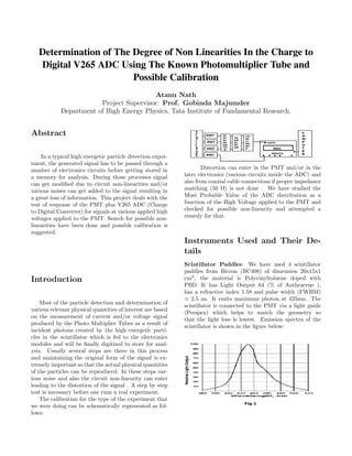
Instruments Used and Their De-
tails
Scintillator Paddles: We have used 4 scintillator
paddles from Bicron (BC408) of dimension 20x15x1
cm3
, the material is Polyvinyltoluene doped with
PBD. It has Light Output 64 (% of Anthracene ),
has a refractive index 1.58 and pulse width (FWHM)
2.5 ns. It emits maximum photon at 425nm. The
scintillator is connected to the PMT via a light guide
(Perspex) which helps to match the geometry so
that the light loss is lowest. Emission spectra of the
scintillator is shown in the figure below:
2. Photomultiplier Tubes: Four PMTs (9807B,
Electron Tubes Limited) for four paddles are used.
It is a 51 mm diameter, end window photomultiplier
with blue-green sensitive bialkali photocathode and
have 12 stages of BeCu dynodes. It is of linear focused
design for good linearity and timing. The curve for
quantum efficiency and the electrical circuit diagram of
the PMT are displayed in Fig.2 and Fig.3 respectively.
Constant Fraction Discriminator (V814): It
is a low threshold constant fraction discriminator
with negative input signals and ECL output. The
threshold of which can be varied from -1mV to -255
mV, in our experiment we set it at 30 mV as the
signals due to Muons are much stronger ( typically
more than 100 mV I have observed), but signal due to
other possible events like scintillation due to electron
strike or PMT dark current are much below 30 mv.
More over P1, P3 and P4 AND Gated pulse was
given as a trigger to the GATE os the ADC to reduce
chance coincidence due to noise trigger. CFD has
got maximum input frequency of 60 MHz, output
width can be varied in the range 6ns-95ns, I have
used 72 ns and that includes most of the significant
part of the signal even including some tail part, an
oscilloscope image describing the situation can be seen
in Fig.4(B). Time delay of this module is 10.5 ± 1.5 ns.
NIM-ECL/ECL-NIM Translator And Fan Out
(V538A): 8 channel accepts ECL/NIM signals and
converts it to NIM/ECL respectively. For each input
there corresponds four output options. ECL signal
frequency < 300MHz (NIM) and < 250MHz (ECL)
signal is accepted in the inputs. Time delay for
ECL-NIM is 2.5-3 ns and for NIM-ECL 3.5-4ns.
Four-fold Coincidence Fan-in/out Translator
(V976): This has 16 inputs and 16 outputs 2-fold, 3-
fold and 4-fold adjustable AND/OR gating is possible,
minimum signal width and also minimum coincidence
width is 2ns, time delay of operation is of 11.5 ns.
Charge Integrating ADC (V265): this has got 8
channels and full-scale of it is 800 pC(12 bit ADC
range), conversion gain 5 counts/pC.
Scematic Diagram of The Experiment
Notations: We use the following notations for clarity:
Signal from PMT-1 of Paddle-1 ≡ P1
Signal from PMT-2 of Paddle-2 ≡ P2
Signal from PMT-3 of Paddle-2 ≡ P3
Signal from PMT-4 of Paddle-2 ≡ P4
All the voltages are in Volts
Details of the connections and operating volt-
ages are given in the table below:
Constant Fraction Dis-
criminator (V814)
Threshold = 30 mV.
Gate width 72 ns.
P1, P3 and P4 are in
the inputs.
PMT-1 of Paddle-1
(Lower most)
HV= 1411 V.
PMT-2 of Paddle-2
(2nd from the bottom)
HV = Variable in my
experiment 1254 V -
1788 V
PMT-3 of Paddle-3
(3rd from the bottom)
HV = 1498 V.
PMT-4 of Paddle-4
(Top most)
HV = 1500V.
Four-fold Coincidence
Fan in Fan out Trans-
lator (V976)
P1, P3 and P4 com-
ing out of the CFD
outputs are three-fold
AND-gated.
Quad Linear Fan in Fan
out (PS Mod.740)
P2 is in the input and 4
outputs are taken in the
output which are P21,
P22, P23, P24.
3. Charge Integrating
ADC (V265)
P21, P22, P23 and P24
are conncetd to the four
channels ch0, ch2, ch4
and ch6. Three-fold
AND-gated output is
fed to the GATE of
the CFD after match-
ing the delays such that
P21, P22, P23, P24 are
well inside 72 ns GATE
trigger pulse.
Linearity Check of PMT and ADC
P21, P22, P23 and P24 are conncetd to the
four channels ch0, ch2, ch4 and ch6, actually out of
the 8 channels odd numbered ones (ch1, ch3, ch5 and
ch 7) happened to be not working well that was tested
in the beginning of this experiment and it was seen
that these odd channels posses no pedastal values
and hence the pedestal positions were undetermined
therefore the even numbered channels were chosen
for the experiment. Typical signal distribution and
corresponding pedestal distribution are displayed in
Fig.5(B) and Fig.5(A) respectively. Where the
signal distribution is fitted with Landau function
and the pedestal is fitted with Gaussian distribution
function, pedestal mean values for the channels 0,2,4
and 6 have been shown in the Table.2.
Channel No Pedestal Value
0 208.2
2 143.5
4 170.00
6 239.4
Two sets of data were taken, in the
first set, for 10 different voltages ADC was
run and the results are shown in Fig.6
First of all these four channels have identical inputs as
these were the 4 outputs of fan-out of the same signal
from Paddle-2, but the graphs shows they are giving
different results, thing to notice is that the points are
differing more and more as we go to higher and higher
voltages, so this clearly show that the channels are
working differently.
Suppose there are N-stages of dynodes in the PMT
and gi and Ri are the gain and resistance for each
stage respectively then the total gain (G) is given by:
G ∝
N
i
gi ∝
N
i
RiV α
ΣRi
= A0V Nα
Final gain of the PMT is the product of gain in each
dynode stage gain, and gain of a stage is proportional
to the applied voltage to that dynode and its previous
stage. This voltage dependence can take complicated
non-linear form but we consider a simple power law for
for this dependence,
M = B0Gβ
= B0(A0V Nα
)β
=> log(M) = p1 log(V ) + p0
Where, p1 = Nαβ and p0 = B0Aβ
0 .
To test our assumption we plot our results in
Log-Log, which is shown in Fig. 7 below.
4. This shows that p1 = Nαβ 7.4 on the average which
is far from 12 and approximately p1 vary 8 %. p1 closed
to 12 (as N=12) was rather expected. So to be sure
of the results we take second set of data considering
the same connections by reconnecting them again.
Second set consists of 6 different voltages but the range
of voltage change kept the same as that of first set,
results for this case are displayed in Fig.8 and Fig.9.
Results (p1 7.5) are not much different from the
first set. Now the question that we can ask is:Is
ADC/PMT Nonlinear ? if yes then both of them
or one of them are non-linear ? And at what extent
they are non-linear?
For a better understanding we needed an al-
ready calibrated ADC. Fortunately we had and
already calibrated QDC (V792N 16 channel QDC)3
,
we repeated our experiment for three channels 6,8 and
14 keeping the earlier situation intact. The result that
we got is displayed in Fig.10 and Fig.11.
Above graphs say p1 11.14 and the point to
notice is that it is the same PMT so α has not changed
its the β that has changed by a factor of 1.5 hence
non-linearity is mainly entering due to the V265 ADC.
So for QDC V792N, p1 = Nα = 11.14 and hence
β 0.673 on the average and particularly for the
channel no. 2 it is 0.665 (which we will need later).
One can think that the Fan-in/out may also contribute
to this results. But this is certainly not the case,
because of two facts, first: the oscilloscope image
shows exactly identical signals, second: 10 shows that
indeed they are identical.
PMT Independent Measurement
This time we took a signal generator and cho-
sen a square pulse of width 10 ns and frequency 10 Hz
(oscilloscope image is shown in Fig.12 ) and fan-out it
two four signals which were finally fed to channel no.
2 of V265ADC and data were taken.
5. A typical ADC distribution along with Gaussian fit
is displayed in Fig.13 below:
Though the pulse was supposed to be 10 ns wide but ac-
tually it is 16 ns at the top and 8 ns at the bottom, the
estimated area under this signal is 16H − 4H = 12H
so charge contained in this puls is 12H/R (where
R = 50Ω) finally for V265 ADC charge contained in
one bin = 0.2 pC hence this pulse will correspond
to ADC bin number 12H/(50 × 0.2) = 1.2H taking
logarithm we get log(ADCPeak) = log(H)+constant.
This line, we expect to describe the ADC be-
haviour in principle, but practically we consider
log(ADCPeak) = β log(H) + constant, but we expect
the slope β to be 1 if the ADC is linear. Following are
the experimental results:
Clearly β 0.651 for channel no. 2. This again
shows that this ADC is non-linear and the QDC
V792N is indeed a good one as we obtained the slope
11.14 for that QDC with PMT from where we obtained
the value of β to be 0.665. But to check V792N with
this pulse method we repeated the same experiment
with this same signal generator pulse and the result is
displayed in Fig.16:
The slope is 1 which strongly suggest that QDC
V792N is definitely linear.
Conclusion
The conclusions those we can draw are:
˙ ADC V265 is non linear.
˙ Our assumed power law successfully describes
the ADC V265 data.
M = B0Gβ
with β 0.651 for channel 2 and each channel
have different β. Through beta we have
quantified the amount of non-linearity.
˙ QDC V265 is linear whcih confirms that the
earlier calibration was right.
Appendix
Tables
set-I V265 ADC (Channel 0)
Voltage Pedestal Separated MPV Error
1254 109.824 ±0.464915
1303 134.957 ±0.524712
1371 198.181 ±0.700580
1422 257.639 ±0.843207
1503 386.879 ±1.22332
1567 508.655 ±1.45834
1604 593.924 ±1.61694
1682 872.7 ±2.29109
1706 976.86 ±2.54258
1788 1410.6 ±3.82075
7. Acknowledgement
I would like to thank Prof. Gobinda Majumder for
his sincere guidance through out the project and for
his help to understand every bit of the experiment. I
am also thankful to Deepak Samuel (Project Scientist)
for his help to understand his codes written for some
of the VME modules. I would also like to thank
my senior Research Scholar Esha Kundu for valuable
discussions and for her earlier calibration of QDC
V792N which helped me to calibrate the V265 ADC. I
thank my colleague Soureek Mitra for his co-operation
and understanding for sharing the same high voltage
supply and for important conceptual discussions.
References
[1] Glenn F. Knoll, Radiation Detection and
Measurement, Third Edition, Reprint 2009.
[2] W. R. Leo, Techniques for Nuclear and
Particle Physics Experiments, Second Revised
Edition, Indian Reprint 2010.
[3] Esha Kundu, Calibration of Versa Module
Europa (VME) Modules , Experimental Project,
February 2011.
[5] CAEN, V265 ADC User Manual.
[6] CAEN, V814 CFD User Manual.
[7] CAEN, V538A ECL-NIM/NIM-ECL Translator
User Manual.
[8] CAEN, V976 Four Fold Coincidence Fan In
Fan Out Translator User Manual.
[9] Phillips Scientific, Quad Linear Fan In Fan Out
User Manual.
[10] CAEN, V792N QDC User Manual
[11] http://my.et-enterprises.com/