Download to read offline

![International Research Journal of Engineering and Technology (IRJET) e-ISSN: 2395-0056
Volume: 06 Issue: 09 | Sep 2019 www.irjet.net p-ISSN: 2395-0072
© 2019, IRJET | Impact Factor value: 7.34 | ISO 9001:2008 Certified Journal | Page 2017
start discharging with different rates depending on the
corresponding input voltage.
Assuming the case where IN1>IN2, Out1 discharges
faster than Out2, the corresponding pMOS transistor (M5)
will turn on initiating the latch regeneration caused by
back-to-back inverters (M3, M5 and M4, M6). Thus, Out2
pulls to VDD and Out1 discharges to ground. If IN1 <IN2,
the circuits works vice versa.
Fig. 1. Circuit diagram of a conventional Single tail
comparator
2.2 DOUBLE TAIL COMPARATOR
The architecture of a Double tail dynamic comparator
which is designed to operate at low voltages is shown in
the figure. It can be observed from figure that the
architecture contains separate input gain stage and output
latch stage. This comparator architecture does not require
too many transistors and are designed to operate at lower
supply voltages when compared to conventional
comparators.
The double tail architecture contains wider Mtail2 for
fast latching and low current in the input stage due to
small Mtail1. This small Mtail1 reduces offset and fast
latching is found to be independent of the input common-
mode voltage (Vcm). At the Reset phase, when CLK=0 both
the tail transistors Mtail1 and Mtail2 are in OFF state
,while M3 and M4 transistors makes the fn and fp nodes to
be charged to VDD denoting the start condition.
During the comparison phase, when CLK=VDD, the tail
transistors becomes ON, while the p-mos transistors M3
and M4 turns OFF. Meanwhile voltages at fn and fp nodes
start to discharge depending on the input voltages. The
two cases depending on the input voltages are: If
VINP>VINN, fn starts discharging at a rate faster than the
node fp, which results more current in M2 than in M1. If
VINN >VINP, fp starts discharging at a rate faster than the
node fn.
The differential voltage builds up, is passed through the
MR1 and MR2 transistors to the back to back cross coupled
inverters and protects the circuit from the adverse effects
of switching noise called kickback noise [3]. With less
stacking, this type of architecture is suited for low supply
voltages. But, during reset phase, fn and fp nodes have to
be charged from ground to VDD, which increases power
consumption.
Fig. 2. Circuit diagram of conventional double tail
comparator
2.3 DOUBLE TAIL COMPARATOR IN 16T
CONFIGURATION
The configuration is named so due to the use of a total of
16 transistors in the circuit. It includes seven pmos and
nine nmos transistors. The 16T configuration includes the
use of two control transistors, two intermediate
transistors and two nmos switches. The introduction of
these additional transistors leads to reduction in the value
of power and delay.
The control transistors in the double tail comparator
with control transistors architecture form a direct current
path from VDD to ground leads to static power
consumption. During the reset phase, both the outputs
which were precharged to VDD is grounded by the
intermediate transistors. Another change in the circuit is
the presence of two nmos switches. In order to minimize
static power, two NMOS switches [Msw1 and Msw2] are
added below the input transistors [IN1 and IN2].
At the beginning of the decision making process, both the
switches are closed, since F1 and F2 nodes are charged to
VDD.
While in evaluation phase nodes F1 and F2 start to reduce
with different discharging rates. Switch in the F2 charging
path is opened in this case, where F2 is pulling up to the
VDD, meanwhile F1 should be discharged completely. This
prevents current drawn from VDD to drop through the F2](https://image.slidesharecdn.com/irjet-v6i9313-191219084658/75/IRJET-A-Novel-High-Speed-Power-Efficient-Double-Tail-Comparator-in-180nm-CMOS-Technology-2-2048.jpg)

![International Research Journal of Engineering and Technology (IRJET) e-ISSN: 2395-0056
Volume: 06 Issue: 09 | Sep 2019 www.irjet.net p-ISSN: 2395-0072
© 2019, IRJET | Impact Factor value: 7.34 | ISO 9001:2008 Certified Journal | Page 2020
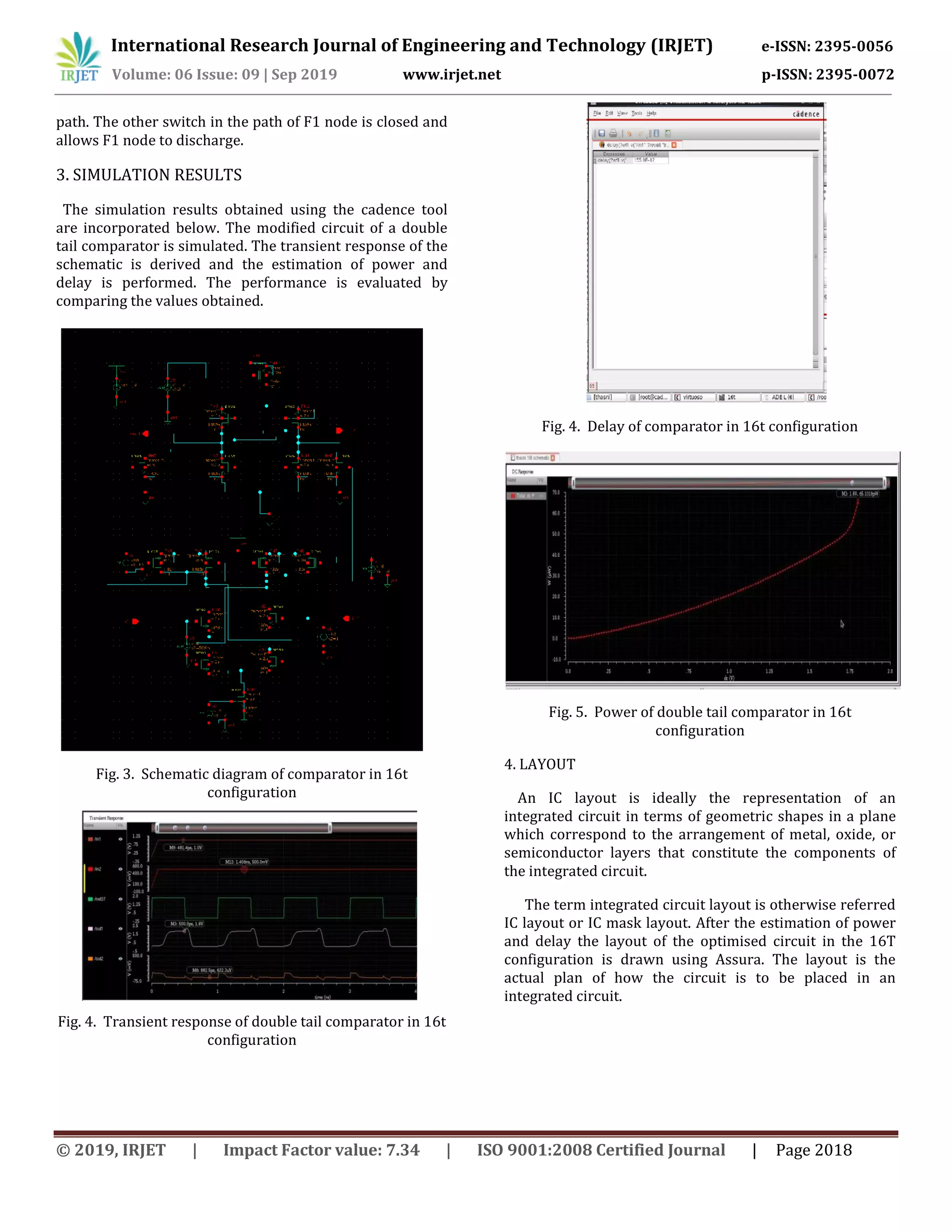
Fig. 9. Result of LVS run
Fig. 10. Tabulation of power and delay values obtained
by simulation
Fig. 11. Comparison of results obtained in simulation
ACKNOWLEDGMENT
This project work would not have been possible without
the sincere assistance of a number of eminent people. I
take this opportunity to acknowledge my heartfelt
gratitude to our respected principal Dr. Jalaja M.J for
providing all the necessary facilities in this institution to
complete my work. I express profound and sincere thanks
to Dr.Leena Mary, the project coordinator and Head of the
Department of Electronics and Communication
Engineering for the valuable supervision.
I am deeply indebted to my guide Mrs.Lekshmi T ,Assistant
Professor, Department of Electronics and Communication
Engg. and Mr.Ben P. Babu, Assistant Professor, Department
of Electronics and Communication Engg., for careful
attention and support to my work.I would like to express
my deepest appreciation to my advisor for helping me to
overcome several constraints. I extend my special thanks
to all my friends for their enthusiastic encouragement and
full support. More than anybody else, I am grateful to my
parents for their encouragement, support, and blessing.
REFERENCES
[1] K. Dinesh, P. Giribabu”Area Efficient Low Power Double
tail Comparator Using SwitchingTransistors, ” IJRAET,
Volume 4, Issue1, APR 2015.
[2] Sri Harsha Gubbala, Venkata Sai Rohit Bhagavatula”
Design of a Single Tail Comparatoron a 90nm Technology,”
International Journal of Engineering Research Technology
(IJERT), ISSN:22780181, IJERTV4IS100269 Vol. 4Issue10,
2015.
[3] Vaishnavi Jumade, Prof. Amol Boke”Designing Of
Double Tail Comparator For HighSpeed Application,”
International Research Journal of Engineering and
Technology (IRJET),e-ISSN: 2395 -0056 Volume: 03 Issue:
04 — Apr-2016.
[4] Rahul Jain, K. Dubey”Design of Low-Power High-Speed
Double-Tail Dynamic CMOSComparator using Novel Latch
Structure, ”IEEE International Conference on Electrical,
Computer and Electronics (UPCON)., IEEE 2017.
[5] Ghazal A. Fahmy”A 6.25ghz, 2.7microwatt, 0.5V,
Double-tail Comparator Using Charge-steering Approach,”
IEEE International Conference on Electrical, Computer and
Electronics (UPCON)., IEEE 2017
[6] Amol D. Shinde, Manish Sharma” Low Power, Area
Efficient Dynamic Comparator With Reduced Activity
Factor,” IEEE International Conference on Electrical,
Computer and Electronics (UPCON).,IEEE 2017.](https://image.slidesharecdn.com/irjet-v6i9313-191219084658/75/IRJET-A-Novel-High-Speed-Power-Efficient-Double-Tail-Comparator-in-180nm-CMOS-Technology-5-2048.jpg)
![International Research Journal of Engineering and Technology (IRJET) e-ISSN: 2395-0056
Volume: 06 Issue: 09 | Sep 2019 www.irjet.net p-ISSN: 2395-0072
© 2019, IRJET | Impact Factor value: 7.34 | ISO 9001:2008 Certified Journal | Page 2021
[7] Shruti Pancholi ,Dr. R.S.Meena” A New Design of a
CMOS Comparator using 45nmTechnology , ”IJISET ,
International Journal of Innovative Science, Engineering
Technology, Vol. 2 Issue 9, September 2015.,IJISET2015.
[8] Nidhi Tarun, Shruti Suman, P. K. Ghosh” Design of Low
Offset and High Speed CMOS Comparator for Analog to
Digital Converter,” IISET, Innovative Systems Design and
Engineering ISSN 2222-1727 (Paper) ISSN 2222-2871
(Online) Vol.5, No.4, 2014.
[9] Yusuke Okaniwa, Hirotaka Tamura,” A 40-Gb/s CMOS
Clocked Comparator With Bandwidth Modulation
Technique,” IEEE JOURNAL OF SOLID-STATE
CIRCUITS,VOL. 40,NO. 8, AUGUST 2005.
[10] Shweta Jadhav, Sujeet Mishra,”A Design of High Speed
and Low Power Clocked Com-parator,” International
Journal of Engineering Science and Computing, November
2016,Volume6 Issue No. 11,IJESC 2016.
[11] Bao-ni Han, Yin-tang Yang, Zhang-ming Zhu,”A Novel
1.25GSPS Ultra High-Speed Comparator in 180nm
CMOS,”International Institute of Microelectronics, Xidian
University, Xian 710071, China, 2016.](https://image.slidesharecdn.com/irjet-v6i9313-191219084658/75/IRJET-A-Novel-High-Speed-Power-Efficient-Double-Tail-Comparator-in-180nm-CMOS-Technology-6-2048.jpg)

This document presents a novel double tail comparator design that aims to improve speed and power efficiency over existing comparator designs. It first discusses conventional comparator designs and their limitations at lower voltages. It then introduces a new 16 transistor double tail comparator configuration that includes control transistors, intermediate transistors, and NMOS switches to reduce power and delay. Simulation results show the transient response and estimate the power and delay of the new design, demonstrating performance improvements over conventional designs. The design was laid out using the Cadence Virtuoso tool.


![[IJET V2I5P8] Authors: Lakshmi K R, Kavitha Issac, Kiran Boby](https://cdn.slidesharecdn.com/ss_thumbnails/ijet-v2i5p8-161107140749-thumbnail.jpg?width=640&height=640&fit=bounds)


![Analysis and design_of_a_low-voltage_low-power[1]](https://cdn.slidesharecdn.com/ss_thumbnails/analysisanddesignofalow-voltagelow-power1-140802050345-phpapp02-thumbnail.jpg?width=640&height=640&fit=bounds)


