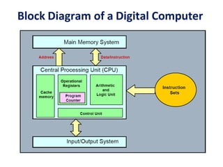
COMPUTER
ORGANIZATION AND
ARCHITECTURE
K.PRASHANTH
Asst. Professor
UNIT-I
•Digital Computers: Introduction, Block diagram of Digital
computer
•Definition of Computer Organization , Computer Design
and Architecture
•Computer Types
•Functional units
•Basic operational concepts
•Bus structures
•Register Transfer Language
•Register transfer
•Bus and Memory Transfers
•Micro Operations (Arithmetic, logical, shift)
•Arithmetic Logic Shift Unit
•Instruction Codes
•Computer Registers
•Computer instructions
•Timing and Control
•Memory Reference instructions
•Input-Output instructions
•Interrupt
3
What is a computer?
• a computer is a sophisticated electronic calculating
machine that:
– Accepts input information,
– Processes the information according to a list of internally
stored instructions and
– Produces the resulting output information.
• Functions performed by a computer are:
– Accepting information to be processed as input.
– Storing a list of instructions to process the information.
– Processing the information according to the list of
instructions.
– Providing the results of the processing as output.
Block Diagram of a Digital Computer
COMPUTER ORGANISATION AND
ARCHITECTURE
• The components from which computers are built,
i.e., computer organization.
• In contrast, computer architecture is the science of
integrating those components to achieve a level of
functionality and performance.
• It is as if computer organization examines the
lumber, bricks, nails, and other building material
• While computer architecture looks at the design of
the house.
Brief History of Computer Evolution
Two phases:
1. before VLSI 1945 – 1978
• ENIAC
• IAS
• IBM
• PDP-8
2. VLSI 1978  present day
• microprocessors !
VLSI = Very Large
Scale Integration
Evolution of Computers
FIRST GENERATION (1945 – 1955)
• Program and data reside in the same memory
(stored program concepts – John von Neumann)
• ALP was made used to write programs
• Vacuum tubes were used to implement the functions
(ALU & CU design)
• Magnetic core and magnetic tape storage devices are
used
• Using electronic vacuum tubes, as the switching
components
SECOND GENERATION (1955 – 1965)
• Transistor were used to design ALU & CU
• HLL is used (FORTRAN)
• To convert HLL to MLL compiler were used
• Separate I/O processor were developed to operate in
parallel with CPU, thus improving the performance
• Invention of the transistor which was faster, smaller
and required considerably less power to operate
• IC technology improved
• Improved IC technology helped in designing low cost, high
speed processor and memory modules
• Multiprogramming, pipelining concepts were incorporated
• DOS allowed efficient and coordinate operation of computer
system with multiple users
• Cache and virtual memory concepts were developed
• More than one circuit on a single silicon chip became
available
THIRD GENERATION (1965-1975)
FOURTH GENERATION (1975-1985)
• CPU – Termed as microprocessor
• INTEL, MOTOROLA, TEXAS,NATIONAL
semiconductors started developing microprocessor
• Workstations, microprocessor (PC) & Notebook
computers were developed
• Interconnection of different computer for better
communication LAN,MAN,WAN
• Computational speed increased by 1000 times
• Specialized processors like Digital Signal Processor
were also developed
• E-Commerce, E- banking, home office
• ARM, AMD, INTEL, MOTOROLA
• High speed processor - GHz speed
• Because of submicron IC technology lot of
added features in small size
BEYOND THE FOURTH GENERATION
(1985 – TILL DATE)
Slide 12
Generations of Progress
Table 3.2 The 5 generations of digital computers, and their ancestors.
Generation
(begun)
Processor
technology
Memory
innovations
I/O devices
introduced
Dominant
look & fell
0 (1600s) (Electro-)
mechanical
Wheel, card Lever, dial,
punched card
Factory
equipment
1 (1950s) Vacuum tube Magnetic
drum
Paper tape,
magnetic tape
Hall-size
cabinet
2 (1960s) Transistor Magnetic
core
Drum, printer,
text terminal
Room-size
mainframe
3 (1970s) SSI/MSI RAM/ROM
chip
Disk, keyboard,
video monitor
Desk-size
mini
4 (1980s) LSI/VLSI SRAM/DRAM Network, CD,
mouse,sound
Desktop/
laptop micro
5 (1990s) ULSI/GSI/
WSI, SOC
SDRAM,
flash
Sensor/actuator,
point/click
Invisible,
embedded
COMPUTER TYPES
Computers are classified based on the
parameters like
• Speed of operation
• Cost
• Computational power
• Type of application
DESK TOP COMPUTER
• Processing &storage units, visual display &audio uits,
keyboards
• Storage media-Hard disks, CD-ROMs
• Eg: Personal computers which is used in homes and offices
• Advantage: Cost effective, easy to operate, suitable for general
purpose educational or business application
NOTEBOOK COMPUTER
• Compact form of personal computer (laptop)
• Advantage is portability
WORK STATIONS
• More computational power than PC
•Costlier
•Used to solve complex problems which arises in engineering
application (graphics, CAD/CAM etc)
ENTERPRISE SYSTEM (MAINFRAME)
•More computational power
•Larger storage capacity
•Used for business data processing in large organization
•Commonly referred as servers or super computers
SERVER SYSTEM
• Supports large volumes of data which frequently need to be
accessed or to be modified
•Supports request response operation
SUPER COMPUTERS
•Faster than mainframes
•Helps in calculating large scale numerical and algorithm
calculation in short span of time
•Used for aircraft design and testing, military application and
weather forecasting
HANDHELD
• Also called a PDA (Personal
Digital Assistant).
• A computer that fits into a
pocket, runs on batteries, and
is used while holding the unit
in your hand.
• Typically used as an
appointment book, address
book, calculator, and notepad.
• Can be synchronized with a
personal microcomputer as a
backup.
Basic Terminology
• Computer
– A device that accepts input,
processes data, stores data, and
produces output, all according to
a series of stored instructions.
• Hardware
– Includes the electronic and
mechanical devices that process
the data; refers to the computer
as well as peripheral devices.
• Software
– A computer program that tells
the computer how to perform
particular tasks.
• Network
– Two or more computers and
other devices that are
connected, for the purpose of
sharing data and programs.
• Peripheral devices
– Used to expand the computer’s
input, output and storage
capabilities.
Basic Terminology
• Input
– Whatever is put into a computer system.
• Data
– Refers to the symbols that represent facts, objects, or ideas.
• Information
– The results of the computer storing data as bits and bytes; the words,
numbers, sounds, and graphics.
• Output
– Consists of the processing results produced by a computer.
• Processing
– Manipulation of the data in many ways.
• Memory
– Area of the computer that temporarily holds data waiting to be processed,
stored, or output.
• Storage
– Area of the computer that holds data on a permanent basis when it is not
immediately needed for processing.
Basic Terminology
•Assembly language program (ALP) – Programs are written using
mnemonics
•Mnemonic – Instruction will be in the form of English like form
•Assembler – is a software which converts ALP to MLL (Machine
Level Language)
•HLL (High Level Language) – Programs are written using English
like statements
•Compiler - Convert HLL to MLL, does this job by reading source
program at once
Basic Terminology
•Interpreter – Converts HLL to MLL, does this job
statement by statement
•System software – Program routines which aid the user
in the execution of programs eg: Assemblers, Compilers
•Operating system – Collection of routines responsible
for controlling and coordinating all the activities in a
computer system
Computing Systems
Computers have two kinds of components:
• Hardware, consisting of its physical devices
(CPU, memory, bus, storage devices, ...)
• Software, consisting of the programs it has
(Operating system, applications, utilities, ...)
Functions of computer
• ALL computer functions are:
– Data PROCESSING
– Data STORAGE
– Data MOVEMENT
– CONTROL
Data = Information
Coordinates How
Information is Used
Functional Units of a Computer
Control
ALU
Memory
Processor
Input
Output
Since 1946 all computers have had 5 components!!!
25
Functional units of a computer
I/O Processor
Output
Memory
Instr1
Instr2
Instr3
Data1
Data2
Input
Control
Arithmetic
& Logic
Input unit accepts
information:
•Human operators,
•Electromechanical devices (keyboard)
•Other computers
Output unit sends
results of processing:
•To a monitor display,
•To a printer
Arithmetic and logic unit(ALU):
•Performs the desired
operations on the input
information as determined
by instructions in the memory
Control unit coordinates
various actions
•Input,
•Output
•Processing
Stores
information:
•Instructions,
•Data
FUNCTIONAL UNITS OF COMPUTER
• Input Unit
• Output Unit
• Central processing Unit (ALU and Control Units)
• Memory
• Bus Structure
INPUT UNIT:
•Converts the external world data to a binary format, which can
be understood by CPU
•Eg: Keyboard, Mouse, Joystick etc
OUTPUT UNIT:
•Converts the binary format data to a format that a common
man can understand
•Eg: Monitor, Printer, LCD, LED etc
28
Input unit
Input Unit
Processor
Memory
Keyboard
Audio input
……
Binary information must be presented to a computer in a specific format. This
task is performed by the input unit:
- Interfaces with input devices.
- Accepts binary information from the input devices.
- Presents this binary information in a format expected by the computer.
- Transfers this information to the memory or processor.
Real world Computer
29
Output unit
•Computers represent information in a specific binary form. Output units:
- Interface with output devices.
- Accept processed results provided by the computer in specific binary form.
- Convert the information in binary form to a form understood by an
output device.
Output Unit
Processor
Memory
Computer Real world
Printer
Graphics display
Speakers
……
CPU
•The “brain” of the machine
•Responsible for carrying out computational task
•Contains ALU, CU, Registers
•ALU Performs Arithmetic and logical operations
•CU Provides control signals in accordance with some
timings which in turn controls the execution process
•Register Stores data and result and speeds up the
operation
31
Arithmetic and logic unit (ALU)
• Operations are executed in the Arithmetic and
Logic Unit (ALU).
– Arithmetic operations such as addition, subtraction.
– Logic operations such as comparison of numbers.
• In order to execute an instruction, operands need
to be brought into the ALU from the memory.
– Operands are stored in general purpose registers available in the ALU.
– Access times of general purpose registers are faster than the cache.
• Results of the operations are stored back in the
memory or retained in the processor for
immediate use.
32
Control unit
• Operation of a computer can be summarized as:
– Accepts information from the input units (Input unit).
– Stores the information (Memory).
– Processes the information (ALU).
– Provides processed results through the output units (Output unit).
• Operations of Input unit, Memory, ALU and
Output unit are coordinated by Control unit.
• Instructions control “what” operations take place
(e.g. data transfer, processing).
• Control unit generates timing signals which
determines “when” a particular operation takes
place.
MEMORY
•Stores data, results, programs
•Two class of storage
(i) Primary (ii) Secondary
•Two types are RAM or R/W memory and ROM read only memory
•ROM is used to store data and program which is not going to change.
•Secondary storage is used for bulk storage or mass storage
34
Memory unit
• Memory unit stores instructions and data.
– Recall, data is represented as a series of bits.
– To store data, memory unit thus stores bits.
• Processor reads instructions and reads/writes
data from/to the memory during the
execution of a program.
– In theory, instructions and data could be fetched one bit at a time.
– In practice, a group of bits is fetched at a time.
– Group of bits stored or retrieved at a time is termed as “word”
– Number of bits in a word is termed as the “word length” of a computer.
• In order to read/write to and from memory, a
processor should know where to look:
– “Address” is associated with each word location.
35
Memory unit (contd..)
• Processor reads/writes to/from memory
based on the memory address:
– Access any word location in a short and fixed amount of time based on the
address.
– Random Access Memory (RAM) provides fixed access time independent of
the location of the word.
– Access time is known as “Memory Access Time”.
• Memory and processor have to
“communicate” with each other in order to
read/write information.
– In order to reduce “communication time”, a small amount of RAM (known as
Cache) is tightly coupled with the processor.
• Modern computers have three to four levels of RAM units with different speeds
and sizes:
– Fastest, smallest known as Cache
– Slowest, largest known as Main memory.
36
Memory unit (contd..)
• Primary storage of the computer consists of RAM units.
– Fastest, smallest unit is Cache.
– Slowest, largest unit is Main Memory.
• Primary storage is insufficient to store large amounts of
data and programs.
– Primary storage can be added, but it is expensive.
• Store large amounts of data on secondary storage
devices:
– Magnetic disks and tapes,
– Optical disks (CD-ROMS).
– Access to the data stored in secondary storage in slower, but take advantage of the fact that
some information may be accessed infrequently.
• Cost of a memory unit depends on its access time,
lesser access time implies higher cost.
MEMORY LOCATIONS AND ADDRESSES
•Main memory is the second major subsystem in a
computer. It consists of a collection of storage locations,
each with a unique identifier, called an address.
•Data is transferred to and from memory in groups of
bits called words. A word can be a group of 8 bits, 16
bits, 32 bits or 64 bits (and growing).
•If the word is 8 bits, it is referred to as a byte. The term
“byte” is so common in computer science that
sometimes a 16-bit word is referred to as a 2-byte word,
or a 32-bit word is referred to as a 4-byte word.
Figure 5.3 Main memory
Memory addresses are defined using unsigned
binary integers.
i
Basic Operational Concepts
Basic Function of Computer
• To Execute a given task as per the appropriate program
• Program consists of list of instructions stored in
memory
Interconnection between Processor and Memory
Registers
Registers are fast stand-alone storage locations that hold data
temporarily. Multiple registers are needed to facilitate the
operation of the CPU. Some of these registers are
 Two registers-MAR (Memory Address Register) and
MDR (Memory Data Register) : To handle the data
transfer between main memory and processor. MAR-
Holds addresses, MDR-Holds data
 Instruction register (IR) : Hold the Instructions that is
currently being executed
 Program counter: Points to the next instructions that is
to be fetched from memory
•(PC) (MAR)( the contents of
PC transferred to MAR)
•(MAR) (Address bus) Select a
particular memory location
•Issues RD control signals
•Reads instruction present in memory
and loaded into MDR
•Will be placed in IR (Contents transferred
from MDR to IR)
•Instruction present in IR will be decoded by
which processor understand what operation it has
to perform
•Increments the contents of PC by 1, so that it
points to the next instruction address
•If data required for operation is available in
register, it performs the operation
•If data is present in memory following sequence
is performed
•Address of the data MAR
•MAR Address bus select memory
location where is issued RD signal
•Reads data via data bus MDR
•From MDR data can be directly routed to ALU or it
can be placed in register and then operation can be
performed
•Results of the operation can be directed towards
output device, memory or register
•Normal execution preempted (interrupt)
BUS STRUCTURE
Connecting CPU and memory
The CPU and memory are normally connected by three
groups of connections, each called a bus: data bus, address
bus and control bus
Connecting CPU and memory using three buses
BUS STRUCTURE
•Group of wires which carries information form CPU to peripherals or vice
– versa
•Single bus structure: Common bus used to communicate between
peripherals and microprocessor
SINGLE BUS STRUCTURE
INPUT MEMORY PROCESSOR OUTPUT
Continued:-
• To improve performance multibus structure can be used
•In two – bus structure : One bus can be used to fetch
instruction other can be used to fetch data, required for
execution.
•Thus improving the performance ,but cost increases
A2 A1 A0 Selected
location
0 0 0 0th Location
0 0 1 1st Location
0 1 0
0 1 1
1 0 0
1 0 1
1 1 0
1 1 1
D0
D0 D7 D7
RD
PROCESSOR
CS
W/R
A0
A1
A2
CONTROL BUS
ADDRESS BUS
DATA BUS
Cont:-
•23 = 8 i.e. 3 address line is required to select 8 location
•In general 2x = n where x number of address lines
(address bit) and n is number of location
•Address bus : unidirectional : group of wires which
carries address information bits form processor to
peripherals (16,20,24 or more parallel signal lines)
Cont:-
•Databus: bidirectional : group of wires which
carries data information bit form processor to
peripherals and vice – versa
•Controlbus: bidirectional: group of wires which
carries control signals form processor to
peripherals and vice – versa
•Figure below shows address, data and control bus
and their connection with peripheral and
microprocessor
PERFORMANCE
•Time taken by the system to execute a program
•Parameters which influence the performance are
•Clock speed
•Type and number of instructions available
•Average time required to execute an instruction
•Memory access time
•Power dissipation in the system
•Number of I/O devices and types of I/O devices connected
•The data transfer capacity of the bus
54
Information in a computer -- Instructions
• Instructions specify commands to:
– Transfer information within a computer (e.g., from
memory to ALU)
– Transfer of information between the computer and I/O
devices (e.g., from keyboard to computer, or computer to
printer)
– Perform arithmetic and logic operations (e.g., Add two
numbers, Perform a logical AND).
• A sequence of instructions to perform a task is
called a program, which is stored in the memory.
• Processor fetches instructions that make up a
program from the memory and performs the
operations stated in those instructions.
55
Information in a computer -- Data
• Data are the “operands” upon which
instructions operate.
• Data could be:
– Numbers,
– Encoded characters.
• Data, in a broad sense means any digital
information.
• Computers use data that is encoded as a string
of binary digits called bits.
56
How are the functional units connected?
•For a computer to achieve its operation, the functional units need to
communicate with each other.
•In order to communicate, they need to be connected.
Memory
Output Processor
Input
Bus
•Functional units may be connected by a group of parallel wires.
•The group of parallel wires is called a bus.
•Each wire in a bus can transfer one bit of information.
•The number of parallel wires in a bus is equal to the word length of
a computer
57
Organization of cache and main
memory
Main
memory Processor
Bus
Cache
memory
Why is the access time of the cache memory lesser than the
access time of the main memory?
Computer Components: Top-Level View
Basic Operational Concepts
Slide 60
Computer Systems and Their Parts
The space of computer systems, with what we normally mean by the
word “computer” highlighted.
Computer
Analog
Fixed-function Stored-program
Electronic Nonelectronic
General-purpose Special-purpose
Number cruncher Data manipulator
Digital
REGISTER TRANSFER LANGUAGE
• The symbolic notation used to describe the micro-operation transfer
among registers is called RTL (Register Transfer Language).
• The information transformed from one register to another register is
represented in symbolic form by replacement operator is called Register
Transfer.
•
The use of symbols instead of a narrative explanation provides an
organized and concise manner for listing the micro-operation sequences in
registers and the control functions that initiate them.
•
A register transfer language is a system for expressing in symbolic form the
microoperation sequences among the registers of a digital module.
• It is a convenient tool for describing the internal organization of digital
computers in concise and precise manner.
• Registers:
•
• Computer registers are designated by upper case letters (and
optionally followed by digits or letters) to denote the function of
the register.
• For example, the register that holds an address for the memory unit
is usually called a memory address register and is designated by the
name MAR.
• Other designations for registers are PC (for program counter), IR
(for instruction register, and R1
• (for processor register).
• The individual flip-flops in an n-bit register are numbered in
sequence from 0 through n-1, starting from 0 in the rightmost
position and increasing the numbers toward the left.
Register Transfer Logic
• Register Transfer:
• Information transfer from one register to another
is designated in symbolic form by means of a
• replacement operator.
• The statement R2← R1 denotes a transfer of the
content of register R1 into register R2.
• It designates a replacement of the content of R2
by the content of R1.
• By definition, the content of the source register R
1 does not change after the transfer.
• If we want the transfer to occur only under a predetermined control
condition then it can be shown by an if-then statement.
•
if (P=1) then R2← R1
•
P is the control signal generated by a control section.
• We can separate the control variables from the register transfer operation
by specifying a Control Function.
• Control function is a Boolean variable that is equal to 0 or 1.
• control function is included in the statement as
• P: R2← R1
• Control condition is terminated by a colon implies transfer operation
be executed by the hardware only if P=1.
• Every statement written in a register transfer notation implies a hardware
construction for implementing the transfer.
Basic symbols of the register transfer
notation
Symbol Description Examples
Letters(and
numerals)
Denotes a register MAR, R2
Parentheses ( )
Denotes a part of a
register R2(0-7), R2(L)
Arrow <-- Denotes transfer of
information
R2 <-- R1
Comma ,
Separates two
microoperations
R2 <- R1, R1<-R2
• A comma is used to separate two or more
operations that are executed at the same
time.
• The statement
(exchange
• T : R2← R1, R1← R2
operation)
• denotes an operation that exchanges the
contents of two rgisters during one common
clock pulse provided that T=1.
•
• Bus and Memory Transfers:
• A more efficient scheme for transferring information
between registers in a multiple-register configuration
is a Common Bus System.
• A common bus consists of a set of common lines, one
for each bit of a register.
Control signals determine which register is selected
by the bus during each particular register transfer.
• Different ways of constructing a Common Bus System
• Using Multiplexers
• Using Tri-state Buffers
• In general a bus system has
•
multiplex “k” Registers
•
each register of “n” bits
• to produce “n-line bus”
• no. of multiplexers required = n
• size of each multiplexer = k x 1
• When the bus is includes in the statement, the register transfer is symbolized as
follows:
• BUS← C, R1← BUS
• The content of register C is placed on the bus, and the content of the bus is loaded
into register R1 by activating its load control input. If the bus is known to exist in
the system, it may be convenient just to show the direct transfer.
• R1← C
• Three-State Bus Buffers:
•
• A bus system can be constructed with three-state gates instead of
multiplexers.
• A three-state gate is a digital circuit that exhibits three states.
• Two of the states are signals equivalent to logic 1 and 0 as in a
conventional gate.
• The third state is a high-impedance state.
• The high-impedance state behaves like an open circuit, which means that
the output is disconnected and does not have logic significance.
• Because of this feature, a large number of three-state gate outputs can be
connected with wires to form a common bus line without endangering
loading effects.
•
The graphic symbol of a three-state buffer gate is shown in Fig. 4-4.
• Memory Transfer:
• The transfer of information from a memory word to the outside
environment is called a read
• operation.
• The transfer of new information to be stored into the memory is
called a write operation.
• A memory word will be symbolized by the letter M.
• The particular memory word among the many available is selected
by the memory address during the transfer.
• It is necessary to specify the address of M when writing memory
transfer operations.
• This will be done by enclosing the address in square brackets
following the letter M.
•
• Consider a memory unit that receives the address from a register,
called the address register, symbolized by AR.
• The data are transferred to another register, called the data register,
symbolized by DR.
• The read operation can be stated as follows:
• Read: DR<- M [AR]
•
• This causes a transfer of information into DR from the memory
word M selected by the address in AR.
• The write operation transfers the content of a data register to a
memory word M selected by the address. Assume that the input
data are in register R1 and the address is in AR.
• The write operation can be stated as follows:
• Write: M [AR] <- R1
Micro-operations
• Types of Micro-operations:
• Register Transfer Micro-operations: Transfer binary information
from one register to another.
• Arithmetic Micro-operations: Perform arithmetic operation on
numeric data stored in registers.
• Logical Micro-operations: Perform bit manipulation operations on
data stored in registers.
• Shift Micro-operations: Perform shift operations on data stored in
registers.
Register Transfer Micro-operation doesn’t change the information
content when the binary information moves from source register to
destination register.
Other three types of micro-operations change the information
change the information content during the transfer.
Arithmetic Micro Operations
•
• The basic arithmetic micro-operations are
• Addition
• Subtraction
• Increment
• Decrement
• Shift
• The arithmetic Micro-operation defined by the statement below specifies the add
micro- operation.
• R3 ← R1 + R2
• It states that the contents of R1 are added to contents of R2 and sum is transferred
to R3.
To implement this statement hardware requires 3 registers and digital
component that performs addition
• Subtraction is most often implemented through complementation and addition.
• The subtract operation is specified by the following statement
• R3 ← R1 + R2 + 1
• instead of minus operator, we can write as
• R2 is the symbol for the 1’s complement of R2
• Adding 1 to 1’s complement produces 2’s complement
• Adding the contents of R1 to the 2's complement of R2 is
equivalent to R1-R2.
• Binary Adder:
• Digital circuit that forms the arithmetic sum of 2 bits and the
previous carry is called FULL ADDER.
• Digital circuit that generates the arithmetic sum of 2 binary
numbers of any lengths is called
• BINARY ADDER.
• Figure 4-6 shows the interconnections of four full-adders (FA) to
provide a 4-bit binary adder.
• The augends bits of A and the addend bits of B are designated by
subscript numbers from right to left, with subscript 0 denoting the
low-order bit.
• The carries are connected in a chain through the full-adders. The
input carry to the binary adder is Co and the output carry is C4. The
S outputs of the full-adders generate the required sum bits.
• An n-bit binary adder requires n full-adders.
• Binary Adder – Subtractor:
• The addition and subtraction operations can be combined into one common circuit
by including an exclusive-OR gate with each full-adder.
• A 4-bit adder-subtractor circuit is shown in Fig. 4-7.
• The mode input M controls the operation. When M = 0 the circuit is an adder and
when M = 1 the circuit becomes a subtractor.
• Each exclusive-OR gate receives input M and one of the inputs of B
• When M = 0, we have B xor 0 = B. The full-adders receive the value of B, the
input carry is 0, and the circuit performs A plus B.
• When M = 1, we have B xor 1 = B' and Co = 1.
• The B inputs are all complemented and a 1 is added through the input carry.
• The circuit performs the operation A plus the 2's complement of B.
Logical Micro Operations
• Logic Micro-operations:
• Logic microoperations specify binary operations for strings
of bits stored in registers.
• These operations consider each bit of the register
separately and treat them as binary variables.
• For example, the exclusive-OR microoperation with the
contents of two registers RI and R2 is symbolized by the
statement
• It specifies a logic microoperation to be executed on the
individual bits of the registers provided that the control
variable P = 1.
• Hardware Implementation:
• The hardware implementation of logic microoperations
requires that logic gates be inserted for each bit or pair of
bits in the registers to perform the required logic function.
• Although there are 16 logic microoperations, most
computers use only four--AND, OR, XOR (exclusive-OR), and
complement from which all others can be derived.
Shift Micro Operations
• Shift microoperations are used for serial transfer of
data.
• The contents of a register can be shifted to the left or
the right.
• During a shift-left operation the serial input transfers a
bit into the rightmost position.
• During a shift-right operation the serial input transfers
a bit into the leftmost position.
• There are three types of shifts: logical, circular, and
arithmetic.
• The symbolic notation for the shift microoperations is
shown in Table 4-7.
• Logical Shift:
• A logical shift is one that transfers 0 through the serial input.
• The symbols shl and shr for logical shift-left and shift-right
microoperations.
The microoperations that specify a 1-bit shift to the left of the
content of register R and a 1-bit shift to the right of the content of
register R shown in table 4.7.
• The bit transferred to the end position through the serial input is
assumed to be 0 during a logical shift.
• Circular Shift:
• The circular shift (also known as a rotate operation) circulates the
bits of the register around the two ends without loss of
information.
• This is accomplished by connecting the serial output of the shift
register to its serial input.
• We will use the symbols cil and cir for the circular shift left and
right, respectively.
• Arithmetic Shift:
• An arithmetic shift is a microoperation that shifts
a signed binary number to the left or right.
• An arithmetic shift-left multiplies a signed binary
number by 2.
• An arithmetic shift-right divides the number by 2.
• Arithmetic shifts must leave the sign bit
unchanged because the sign of the number
remains the same when it is multiplied or divided
by 2.
Arithmetic Logic Shift Unit
• Instead of having individual registers performing the
microoperations directly, computer systems employ a number of
storage registers connected to a common operational unit called an
arithmetic logic unit, abbreviated ALU.
• The ALU is a combinational circuit so that the entire register
transfer operation from the
• source registers through the ALU and into the destination register
can be performed during one clock pulse period.
• The shift microoperations are often performed in a separate unit,
but sometimes the shift unit is made part of the overall ALU.
• The arithmetic, logic, and shift circuits introduced in previous
sections can be combined into one ALU with common selection
variables. One stage of an arithmetic logic shift unit is shown in Fig.
4- 13.
• Particular microoperation is selected with inputs S1 and S0. A 4 x 1
multiplexer at the output chooses between an arithmetic output in
Di and a logic output in Ei.
• The data in the multiplexer are selected with inputs S3 and S2. The
other two data inputs to the multiplexer receive inputs Ai-1 for the
shift-right operation and Ai+1 for the shift-left operation.
• The circuit whose one stage is specified in Fig. 4-13 provides eight
arithmetic operation, four logic operations, and two shift
operations.
• Each operation is selected with the five variables S3, S2, S1, S0 and
Cin.
• The input carry Cin is used for selecting an arithmetic operation
only.
90
Instruction Codes
• Instruction:
• Instructions specify commands to:
– Transfer information within a computer (e.g., from memory to
ALU)
– Transfer of information between the computer and I/O devices
(e.g., from keyboard to computer, or computer to printer)
– Perform arithmetic and logic operations (e.g., Add two numbers,
Perform a logical AND).
• A sequence of instructions to perform a task is called a
program, which is stored in the memory.
• Processor fetches instructions that make up a program
from the memory and performs the operations stated
in those instructions.
Instruction Codes
● The organization of the computer is defined by its
internal registers, the timing and control structure,
and the set of instructions that it uses.
● A computer instruction is a binary code that
specifies a sequence of microoperations for the
computer.
● An instruction code is a group of bits that instruct
the computer to perform a specific operation.
● Instruction code is usually divided into two parts.
○ Operation part - Group of bits that define such
operations as add, subtract, multiply, shift, and
complement.
○ Address part - Contains registers or memory words
where the address of operand is found or the result is to
be stored.
● Each computer has its own instruction code format.
Operation Code
● The operation code(op-code) of an
instruction is a group of bits that define such
operations as add, subtract, multiply, shift,
and complement.
● The number of bits required for the operation
code of an instruction depends on the total
number of operations available in the
computer.(n bits for 2n operations)
● An operation code is sometimes called a
macro-operation because it specifies a set
of micro-operations.
Stored Program Organization
● Simplest way to organize computer is to have
one processor register(Accumulator AC) and an
instruction code format with two parts.
○ First-Operation to be performed(Opcode)
○ Second – Address
● The memory address tells the control where to
find an operand in memory.
● This operand is read from memory and used as
the data to be operated on together with the
data stored in the processor register.
● Instructions are stored
in one section of the
memory and data in
another.
● For a memory unit with
4096 words we need 12
bits to specify an
address since
212=4096.
● 4 bits are available for
opcode to specify one
out of 16 possible
operations.
● The control reads a 16-bit instruction from
the program portion of memory.
● It uses the 12-bit address part of the
instruction to read a 16-bit operand from
the data portion of memory.
● It then executes the operation specified
by the operation code.
● The operation is performed with the
memory operand and the content of AC.
Computer Registers
Need of Registers?
● Computer instructions are normally stored in consecutive memory
locations and are executed sequentially one at a time.
● The control reads an instruction from a specific address in memory
and executes it. It then continues by reading the next instruction in
sequence and executes it, and so on.
● This type of instruction sequencing needs a counter to calculate
the address of the next instruction after execution of the current
instruction is completed.
● It is also necessary to provide a register in the control unit for
storing the instruction code after it is read from memory.
● The computer needs processor registers for manipulating data and
a register for holding a memory address.
List of basic Registers
Code Bits Name Purpose
DR 16 Data Register Holds memory operand
AR 12 Address register Holds address for memory
AC 16 Accumulator Processor register
IR 16 Instruction register Holds instruction code
PC 12 Program counter Holds address of instruction
TR 16 Temporary register Holds temporary data
INPR 8 Input register Holds input character
OUTR 8 Output register Holds output character
Common Bus System
Need of Common Bus System ?
● The basic computer has eight registers, a memory
unit, and a control unit.
● Paths must be provided to transfer information from
one register to another and between memory and
registers.
● The number of wires will be excessive if connections
are made between the outputs of each register and
the inputs of the other registers.
● Hence more efficient scheme with a common bus is
used.
● The outputs of seven registers and memory are connected to
the common bus.
● The specific output that is selected for the bus lines at any
given time is determined from the binary value of the
selection variables S2, S1, and S0.
● The number along each output shows the decimal equivalent
of the required binary selection.
● For example, the number along the output of DR is 3. The
16-bit outputs of DR are placed on the bus lines when
S2S1S0 =011 since this is the binary value of decimal 3.
● The lines from the common bus are connected to the inputs
of each register and the data inputs of the memory.
● The particular register whose LD (load) input is enabled
receives the data from the bus during the next clock pulse
transition.
● The memory receives the contents of the bus when its write
input is activated.
● The memory places its 16-bit output onto the bus when the
read input is activated and S2S1S0 =111.
● INPR is connected to provide information to the bus
but OUTR can only receive information from the bus.
● This is because INPR receives a character from an
input device which is then transferred to AC.
● OUTR receives a character from AC and delivers it to
an output device.
● There is no transfer from OUTR to any of the other
registers.
● The inputs of AC come from an adder and logic
circuit.
● This circuit has three sets of inputs.
● One set of 16-bit inputs come from the outputs of AC.
They are used to implement register micro-operations
such as complement AC and shift AC.
● Another set of 16-bit inputs come from the data
regisler DR. The inputs from DR and AC are used for
arithmetic and logic microoperations.
● A third set of 8-bit inputs come from the input register
INPR.
Computer
Instructions
Instruction Cycle
• The processing required for a single instruction is called an
instruction cycle.
• The CPU performs a sequence of micro operations for each
instruction. The sequence for each instruction of the Basic
Computer can be refined into 4 abstract phases:
• 1. Fetch instruction
• 2. Decode
• 3. Fetch operand
• 4. Execute
• ADD LocationA, LocationB
• This instruction adds the contents of memory
locationA and Contents of memory locationB in 3
instruction cycles.
• The program fragment shown adds the contents
of the memory word at address 940 to the
contents of the memory word at address 941 and
stores the result in the latter location.
• Three instructions, which can be described as
three fetch and three execute cycles, are required
INSTRUCTION CYCLE
INSTRUCTION CYCLE
• Program execution can be represented in above
figure:
• Instruction 1
step1. Fetch instruction1
step2. Execute instruction1
• Instruction 2
step3. Fetch instruction2
step4. Execute instruction2
• Instruction 3
step5. Fetch instruction3
step6. Execute instruction3
1. The PC contains 300, the address of the first instruction.
This instruction (the value 1940 in hexadecimal) is
loaded into the instruction register IR, and the PC is
incremented.
2. The first 4 bits (first hexadecimal digit) in the IR indicate
that the AC is to be loaded. The remaining 12 bits (three
hexadecimal digits) specify the address (940) from
which data are to be loaded.
3. The next instruction (5941) is fetched from location 301,
and the PC is incremented.
4. The old contents of the AC and the contents of location
941 are added, and the result is stored in the AC.
5. The next instruction (2941) is fetched from location 302,
and the PC is incremented.
6. The contents of the AC are stored in location 941.
Instruction Format
● The basic computer has three instruction
code formats each having 16 bits
○ Memory reference instructions
○ Register reference instructions
○ I/O instructions
● The opcode part of the instruction contains
three bits and the meaning of the remaining
13 bits depends on the operation code
encountered.
Memory reference instructions
● Bits 0-11 for specifying address.
● Bits 12-14 for specifying opcode.
● 15th bit specifies addressing modes. (0 for direct
and 1 for indirect)
● Opcode=000 through 110
● I=0 or 1
● Eg:
○ AND - 0xxx(direct) or 8xxx(indirect)
○ ADD - 1xxx or 9xxx
Register reference instructions
● Recognized by the operation code 111 with a 0 in the
15th bit of the instruction.
● Specifies an operation on or a test of the AC register.
● An operand from memory is not needed.
● Therefore the 12 bits are used to specify the operation
to be executed.
● Eg:
○ CLA - 7800 : Clear AC
○ CLE - 7400 : Clear E
I/O instructions
● These instructions are needed for transfering
informations to and from AC register.
● Recognized by the opcode 111 and a 1 in the
15th bit.
● Bits 0-11 specify the type of I/O Operation
performed.
● Eg:
○ INP - F800 : Input characters to AC
○ OUT - F400 : Output characters from AC
Instruction Set Completeness
● The set of instructions are said to be
complete if the computer includes a sufficient
number of instructions in each of the
following categories
a. Arithmetic, logical, and shift instructions
b. Instructions for moving information to and from
memory and processor registers
c. Program control instructions
d. Input and output instructions
Timing and
Control
Timing and Control
● The timing for all registers in the basic computer
is controlled by a master clock generator.
● The clock pulses are applied to all flip-flops and
registers.
● The clock pulses do not change the state of a
register unless the register is enabled by a
control signal.
● Two major types of control organization:
○ hardwired control
○ microprogrammed control.
Example
Add R1, R2
T1
T2
T3
T4
Enable R1
Enable R2
Enable ALU for addition operation
•Control unit works with a
reference signal called
processor clock
•Processor divides the
operations into basic steps
•Each basic step is
executed in one clock
cycle
T1
T2
R1 R2
R2
Hardwired Control
● The control logic is
implemented with
gates, flip-flops,
decoders, and other
digital circuits.
● It can be optimized to
produce a fast mode of
operation.
● Requires changes in the
wiring among the
various components if
the design has to be
modified or changed.
Microprogrammed Control
● The control information
is stored in a control
memory.
● The control memory is
programmed to initiate
the required sequence
of microoperations.
● Required changes or
modifications can be
done by updating the
microprogram in
control memory.
● Consists of two decoders, a sequence counter, and a
number of control logic gates.
● An instruction read from memory is placed in the
instruction register(IR).
● The IR is divided into three parts:
○ I bit, opcode, and Address bits.
● Op-code in 12-14 bits are decoded with a 3x8
decoder.
● 8 outputs of the decoder are designated by the
symbols D0 through D7.
● Bit 15 is transferred to a flip-flop I.
● Bits 0-11 are applied to the control logic gates.
Hardwired control unit
● The 4-bit sequence counter can count in binary from 0-
15.
● The outputs of the counter are decoded into 16 timing
signals T0-T15.
● The sequence counter SC can be incremented or
cleared synchronously.
● Mostly,SC is incremented to provide the sequence of
timing signals(T1,T2,...,T15)
● Once in a while, the counter is cleared to 0, causing
the next active timing signal to be T0.
● Eg: Suppose,at time T4, SC is cleared to 0 if decoder
output D3 is active. D3T4: SC ← 0.
Hardwired control unit
● The SC responds to the positive transition of the
clock.
● Initially, the CLR input of SC is active.
● Hence it clears SC to 0, giving the timing signal T0
out of the decoder.
● T0 is active during one clock cycle and will trigger
only those registers whose control inputs are
connected to timing signal T0.
● SC is incremented with every positive clock
transition, unless its CLR input is active.
● This produces the sequence of timing signals T0, T1,
T2, T3, T4 up to T15 and back to T0.
Hardwired control unit
Interrupt
• When the external device becomes ready to be
serviced— then the external device sends an interrupt
request signal to the processor. The processor
responds by suspending operation of the current
program
• With interrupts, the processor can be engaged in
executing other instructions while an I/O operation is
in progress and resumes the original execution after
the device is serviced.
• Processor provides requested service by executing
interrupt service routine (ISR)
• Contents of PC, general registers, and some control
information are stored in memory .
• When ISR completed, processor restored, so that
interrupted program may continue
• It suspends execution of the current program
being executed and saves its context. This
means saving the address of the next
instruction to be executed
END OF UNIT 1

computer organisation architecture.pptx

  • 1.
  • 2.
    UNIT-I •Digital Computers: Introduction,Block diagram of Digital computer •Definition of Computer Organization , Computer Design and Architecture •Computer Types •Functional units •Basic operational concepts •Bus structures •Register Transfer Language •Register transfer •Bus and Memory Transfers •Micro Operations (Arithmetic, logical, shift) •Arithmetic Logic Shift Unit •Instruction Codes •Computer Registers •Computer instructions •Timing and Control •Memory Reference instructions •Input-Output instructions •Interrupt
  • 3.
    3 What is acomputer? • a computer is a sophisticated electronic calculating machine that: – Accepts input information, – Processes the information according to a list of internally stored instructions and – Produces the resulting output information. • Functions performed by a computer are: – Accepting information to be processed as input. – Storing a list of instructions to process the information. – Processing the information according to the list of instructions. – Providing the results of the processing as output.
  • 4.
    Block Diagram ofa Digital Computer
  • 5.
    COMPUTER ORGANISATION AND ARCHITECTURE •The components from which computers are built, i.e., computer organization. • In contrast, computer architecture is the science of integrating those components to achieve a level of functionality and performance. • It is as if computer organization examines the lumber, bricks, nails, and other building material • While computer architecture looks at the design of the house.
  • 6.
    Brief History ofComputer Evolution Two phases: 1. before VLSI 1945 – 1978 • ENIAC • IAS • IBM • PDP-8 2. VLSI 1978  present day • microprocessors ! VLSI = Very Large Scale Integration
  • 7.
    Evolution of Computers FIRSTGENERATION (1945 – 1955) • Program and data reside in the same memory (stored program concepts – John von Neumann) • ALP was made used to write programs • Vacuum tubes were used to implement the functions (ALU & CU design) • Magnetic core and magnetic tape storage devices are used • Using electronic vacuum tubes, as the switching components
  • 8.
    SECOND GENERATION (1955– 1965) • Transistor were used to design ALU & CU • HLL is used (FORTRAN) • To convert HLL to MLL compiler were used • Separate I/O processor were developed to operate in parallel with CPU, thus improving the performance • Invention of the transistor which was faster, smaller and required considerably less power to operate
  • 9.
    • IC technologyimproved • Improved IC technology helped in designing low cost, high speed processor and memory modules • Multiprogramming, pipelining concepts were incorporated • DOS allowed efficient and coordinate operation of computer system with multiple users • Cache and virtual memory concepts were developed • More than one circuit on a single silicon chip became available THIRD GENERATION (1965-1975)
  • 10.
    FOURTH GENERATION (1975-1985) •CPU – Termed as microprocessor • INTEL, MOTOROLA, TEXAS,NATIONAL semiconductors started developing microprocessor • Workstations, microprocessor (PC) & Notebook computers were developed • Interconnection of different computer for better communication LAN,MAN,WAN • Computational speed increased by 1000 times • Specialized processors like Digital Signal Processor were also developed
  • 11.
    • E-Commerce, E-banking, home office • ARM, AMD, INTEL, MOTOROLA • High speed processor - GHz speed • Because of submicron IC technology lot of added features in small size BEYOND THE FOURTH GENERATION (1985 – TILL DATE)
  • 12.
    Slide 12 Generations ofProgress Table 3.2 The 5 generations of digital computers, and their ancestors. Generation (begun) Processor technology Memory innovations I/O devices introduced Dominant look & fell 0 (1600s) (Electro-) mechanical Wheel, card Lever, dial, punched card Factory equipment 1 (1950s) Vacuum tube Magnetic drum Paper tape, magnetic tape Hall-size cabinet 2 (1960s) Transistor Magnetic core Drum, printer, text terminal Room-size mainframe 3 (1970s) SSI/MSI RAM/ROM chip Disk, keyboard, video monitor Desk-size mini 4 (1980s) LSI/VLSI SRAM/DRAM Network, CD, mouse,sound Desktop/ laptop micro 5 (1990s) ULSI/GSI/ WSI, SOC SDRAM, flash Sensor/actuator, point/click Invisible, embedded
  • 13.
    COMPUTER TYPES Computers areclassified based on the parameters like • Speed of operation • Cost • Computational power • Type of application
  • 14.
    DESK TOP COMPUTER •Processing &storage units, visual display &audio uits, keyboards • Storage media-Hard disks, CD-ROMs • Eg: Personal computers which is used in homes and offices • Advantage: Cost effective, easy to operate, suitable for general purpose educational or business application NOTEBOOK COMPUTER • Compact form of personal computer (laptop) • Advantage is portability
  • 15.
    WORK STATIONS • Morecomputational power than PC •Costlier •Used to solve complex problems which arises in engineering application (graphics, CAD/CAM etc) ENTERPRISE SYSTEM (MAINFRAME) •More computational power •Larger storage capacity •Used for business data processing in large organization •Commonly referred as servers or super computers
  • 16.
    SERVER SYSTEM • Supportslarge volumes of data which frequently need to be accessed or to be modified •Supports request response operation SUPER COMPUTERS •Faster than mainframes •Helps in calculating large scale numerical and algorithm calculation in short span of time •Used for aircraft design and testing, military application and weather forecasting
  • 17.
    HANDHELD • Also calleda PDA (Personal Digital Assistant). • A computer that fits into a pocket, runs on batteries, and is used while holding the unit in your hand. • Typically used as an appointment book, address book, calculator, and notepad. • Can be synchronized with a personal microcomputer as a backup.
  • 18.
    Basic Terminology • Computer –A device that accepts input, processes data, stores data, and produces output, all according to a series of stored instructions. • Hardware – Includes the electronic and mechanical devices that process the data; refers to the computer as well as peripheral devices. • Software – A computer program that tells the computer how to perform particular tasks. • Network – Two or more computers and other devices that are connected, for the purpose of sharing data and programs. • Peripheral devices – Used to expand the computer’s input, output and storage capabilities.
  • 19.
    Basic Terminology • Input –Whatever is put into a computer system. • Data – Refers to the symbols that represent facts, objects, or ideas. • Information – The results of the computer storing data as bits and bytes; the words, numbers, sounds, and graphics. • Output – Consists of the processing results produced by a computer. • Processing – Manipulation of the data in many ways. • Memory – Area of the computer that temporarily holds data waiting to be processed, stored, or output. • Storage – Area of the computer that holds data on a permanent basis when it is not immediately needed for processing.
  • 20.
    Basic Terminology •Assembly languageprogram (ALP) – Programs are written using mnemonics •Mnemonic – Instruction will be in the form of English like form •Assembler – is a software which converts ALP to MLL (Machine Level Language) •HLL (High Level Language) – Programs are written using English like statements •Compiler - Convert HLL to MLL, does this job by reading source program at once
  • 21.
    Basic Terminology •Interpreter –Converts HLL to MLL, does this job statement by statement •System software – Program routines which aid the user in the execution of programs eg: Assemblers, Compilers •Operating system – Collection of routines responsible for controlling and coordinating all the activities in a computer system
  • 22.
    Computing Systems Computers havetwo kinds of components: • Hardware, consisting of its physical devices (CPU, memory, bus, storage devices, ...) • Software, consisting of the programs it has (Operating system, applications, utilities, ...)
  • 23.
    Functions of computer •ALL computer functions are: – Data PROCESSING – Data STORAGE – Data MOVEMENT – CONTROL Data = Information Coordinates How Information is Used
  • 24.
    Functional Units ofa Computer Control ALU Memory Processor Input Output Since 1946 all computers have had 5 components!!!
  • 25.
    25 Functional units ofa computer I/O Processor Output Memory Instr1 Instr2 Instr3 Data1 Data2 Input Control Arithmetic & Logic Input unit accepts information: •Human operators, •Electromechanical devices (keyboard) •Other computers Output unit sends results of processing: •To a monitor display, •To a printer Arithmetic and logic unit(ALU): •Performs the desired operations on the input information as determined by instructions in the memory Control unit coordinates various actions •Input, •Output •Processing Stores information: •Instructions, •Data
  • 26.
    FUNCTIONAL UNITS OFCOMPUTER • Input Unit • Output Unit • Central processing Unit (ALU and Control Units) • Memory • Bus Structure
  • 27.
    INPUT UNIT: •Converts theexternal world data to a binary format, which can be understood by CPU •Eg: Keyboard, Mouse, Joystick etc OUTPUT UNIT: •Converts the binary format data to a format that a common man can understand •Eg: Monitor, Printer, LCD, LED etc
  • 28.
    28 Input unit Input Unit Processor Memory Keyboard Audioinput …… Binary information must be presented to a computer in a specific format. This task is performed by the input unit: - Interfaces with input devices. - Accepts binary information from the input devices. - Presents this binary information in a format expected by the computer. - Transfers this information to the memory or processor. Real world Computer
  • 29.
    29 Output unit •Computers representinformation in a specific binary form. Output units: - Interface with output devices. - Accept processed results provided by the computer in specific binary form. - Convert the information in binary form to a form understood by an output device. Output Unit Processor Memory Computer Real world Printer Graphics display Speakers ……
  • 30.
    CPU •The “brain” ofthe machine •Responsible for carrying out computational task •Contains ALU, CU, Registers •ALU Performs Arithmetic and logical operations •CU Provides control signals in accordance with some timings which in turn controls the execution process •Register Stores data and result and speeds up the operation
  • 31.
    31 Arithmetic and logicunit (ALU) • Operations are executed in the Arithmetic and Logic Unit (ALU). – Arithmetic operations such as addition, subtraction. – Logic operations such as comparison of numbers. • In order to execute an instruction, operands need to be brought into the ALU from the memory. – Operands are stored in general purpose registers available in the ALU. – Access times of general purpose registers are faster than the cache. • Results of the operations are stored back in the memory or retained in the processor for immediate use.
  • 32.
    32 Control unit • Operationof a computer can be summarized as: – Accepts information from the input units (Input unit). – Stores the information (Memory). – Processes the information (ALU). – Provides processed results through the output units (Output unit). • Operations of Input unit, Memory, ALU and Output unit are coordinated by Control unit. • Instructions control “what” operations take place (e.g. data transfer, processing). • Control unit generates timing signals which determines “when” a particular operation takes place.
  • 33.
    MEMORY •Stores data, results,programs •Two class of storage (i) Primary (ii) Secondary •Two types are RAM or R/W memory and ROM read only memory •ROM is used to store data and program which is not going to change. •Secondary storage is used for bulk storage or mass storage
  • 34.
    34 Memory unit • Memoryunit stores instructions and data. – Recall, data is represented as a series of bits. – To store data, memory unit thus stores bits. • Processor reads instructions and reads/writes data from/to the memory during the execution of a program. – In theory, instructions and data could be fetched one bit at a time. – In practice, a group of bits is fetched at a time. – Group of bits stored or retrieved at a time is termed as “word” – Number of bits in a word is termed as the “word length” of a computer. • In order to read/write to and from memory, a processor should know where to look: – “Address” is associated with each word location.
  • 35.
    35 Memory unit (contd..) •Processor reads/writes to/from memory based on the memory address: – Access any word location in a short and fixed amount of time based on the address. – Random Access Memory (RAM) provides fixed access time independent of the location of the word. – Access time is known as “Memory Access Time”. • Memory and processor have to “communicate” with each other in order to read/write information. – In order to reduce “communication time”, a small amount of RAM (known as Cache) is tightly coupled with the processor. • Modern computers have three to four levels of RAM units with different speeds and sizes: – Fastest, smallest known as Cache – Slowest, largest known as Main memory.
  • 36.
    36 Memory unit (contd..) •Primary storage of the computer consists of RAM units. – Fastest, smallest unit is Cache. – Slowest, largest unit is Main Memory. • Primary storage is insufficient to store large amounts of data and programs. – Primary storage can be added, but it is expensive. • Store large amounts of data on secondary storage devices: – Magnetic disks and tapes, – Optical disks (CD-ROMS). – Access to the data stored in secondary storage in slower, but take advantage of the fact that some information may be accessed infrequently. • Cost of a memory unit depends on its access time, lesser access time implies higher cost.
  • 37.
    MEMORY LOCATIONS ANDADDRESSES •Main memory is the second major subsystem in a computer. It consists of a collection of storage locations, each with a unique identifier, called an address. •Data is transferred to and from memory in groups of bits called words. A word can be a group of 8 bits, 16 bits, 32 bits or 64 bits (and growing). •If the word is 8 bits, it is referred to as a byte. The term “byte” is so common in computer science that sometimes a 16-bit word is referred to as a 2-byte word, or a 32-bit word is referred to as a 4-byte word.
  • 38.
  • 39.
    Memory addresses aredefined using unsigned binary integers. i
  • 40.
    Basic Operational Concepts BasicFunction of Computer • To Execute a given task as per the appropriate program • Program consists of list of instructions stored in memory
  • 41.
  • 42.
    Registers Registers are faststand-alone storage locations that hold data temporarily. Multiple registers are needed to facilitate the operation of the CPU. Some of these registers are  Two registers-MAR (Memory Address Register) and MDR (Memory Data Register) : To handle the data transfer between main memory and processor. MAR- Holds addresses, MDR-Holds data  Instruction register (IR) : Hold the Instructions that is currently being executed  Program counter: Points to the next instructions that is to be fetched from memory
  • 43.
    •(PC) (MAR)( thecontents of PC transferred to MAR) •(MAR) (Address bus) Select a particular memory location •Issues RD control signals •Reads instruction present in memory and loaded into MDR •Will be placed in IR (Contents transferred from MDR to IR)
  • 44.
    •Instruction present inIR will be decoded by which processor understand what operation it has to perform •Increments the contents of PC by 1, so that it points to the next instruction address •If data required for operation is available in register, it performs the operation •If data is present in memory following sequence is performed
  • 45.
    •Address of thedata MAR •MAR Address bus select memory location where is issued RD signal •Reads data via data bus MDR •From MDR data can be directly routed to ALU or it can be placed in register and then operation can be performed •Results of the operation can be directed towards output device, memory or register •Normal execution preempted (interrupt)
  • 46.
    BUS STRUCTURE Connecting CPUand memory The CPU and memory are normally connected by three groups of connections, each called a bus: data bus, address bus and control bus Connecting CPU and memory using three buses
  • 47.
    BUS STRUCTURE •Group ofwires which carries information form CPU to peripherals or vice – versa •Single bus structure: Common bus used to communicate between peripherals and microprocessor SINGLE BUS STRUCTURE INPUT MEMORY PROCESSOR OUTPUT
  • 48.
    Continued:- • To improveperformance multibus structure can be used •In two – bus structure : One bus can be used to fetch instruction other can be used to fetch data, required for execution. •Thus improving the performance ,but cost increases
  • 49.
    A2 A1 A0Selected location 0 0 0 0th Location 0 0 1 1st Location 0 1 0 0 1 1 1 0 0 1 0 1 1 1 0 1 1 1 D0 D0 D7 D7 RD PROCESSOR CS W/R A0 A1 A2 CONTROL BUS ADDRESS BUS DATA BUS
  • 50.
    Cont:- •23 = 8i.e. 3 address line is required to select 8 location •In general 2x = n where x number of address lines (address bit) and n is number of location •Address bus : unidirectional : group of wires which carries address information bits form processor to peripherals (16,20,24 or more parallel signal lines)
  • 51.
    Cont:- •Databus: bidirectional :group of wires which carries data information bit form processor to peripherals and vice – versa •Controlbus: bidirectional: group of wires which carries control signals form processor to peripherals and vice – versa •Figure below shows address, data and control bus and their connection with peripheral and microprocessor
  • 53.
    PERFORMANCE •Time taken bythe system to execute a program •Parameters which influence the performance are •Clock speed •Type and number of instructions available •Average time required to execute an instruction •Memory access time •Power dissipation in the system •Number of I/O devices and types of I/O devices connected •The data transfer capacity of the bus
  • 54.
    54 Information in acomputer -- Instructions • Instructions specify commands to: – Transfer information within a computer (e.g., from memory to ALU) – Transfer of information between the computer and I/O devices (e.g., from keyboard to computer, or computer to printer) – Perform arithmetic and logic operations (e.g., Add two numbers, Perform a logical AND). • A sequence of instructions to perform a task is called a program, which is stored in the memory. • Processor fetches instructions that make up a program from the memory and performs the operations stated in those instructions.
  • 55.
    55 Information in acomputer -- Data • Data are the “operands” upon which instructions operate. • Data could be: – Numbers, – Encoded characters. • Data, in a broad sense means any digital information. • Computers use data that is encoded as a string of binary digits called bits.
  • 56.
    56 How are thefunctional units connected? •For a computer to achieve its operation, the functional units need to communicate with each other. •In order to communicate, they need to be connected. Memory Output Processor Input Bus •Functional units may be connected by a group of parallel wires. •The group of parallel wires is called a bus. •Each wire in a bus can transfer one bit of information. •The number of parallel wires in a bus is equal to the word length of a computer
  • 57.
    57 Organization of cacheand main memory Main memory Processor Bus Cache memory Why is the access time of the cache memory lesser than the access time of the main memory?
  • 58.
  • 59.
  • 60.
    Slide 60 Computer Systemsand Their Parts The space of computer systems, with what we normally mean by the word “computer” highlighted. Computer Analog Fixed-function Stored-program Electronic Nonelectronic General-purpose Special-purpose Number cruncher Data manipulator Digital
  • 61.
    REGISTER TRANSFER LANGUAGE •The symbolic notation used to describe the micro-operation transfer among registers is called RTL (Register Transfer Language). • The information transformed from one register to another register is represented in symbolic form by replacement operator is called Register Transfer. • The use of symbols instead of a narrative explanation provides an organized and concise manner for listing the micro-operation sequences in registers and the control functions that initiate them. • A register transfer language is a system for expressing in symbolic form the microoperation sequences among the registers of a digital module. • It is a convenient tool for describing the internal organization of digital computers in concise and precise manner.
  • 62.
    • Registers: • • Computerregisters are designated by upper case letters (and optionally followed by digits or letters) to denote the function of the register. • For example, the register that holds an address for the memory unit is usually called a memory address register and is designated by the name MAR. • Other designations for registers are PC (for program counter), IR (for instruction register, and R1 • (for processor register). • The individual flip-flops in an n-bit register are numbered in sequence from 0 through n-1, starting from 0 in the rightmost position and increasing the numbers toward the left.
  • 64.
    Register Transfer Logic •Register Transfer: • Information transfer from one register to another is designated in symbolic form by means of a • replacement operator. • The statement R2← R1 denotes a transfer of the content of register R1 into register R2. • It designates a replacement of the content of R2 by the content of R1. • By definition, the content of the source register R 1 does not change after the transfer.
  • 65.
    • If wewant the transfer to occur only under a predetermined control condition then it can be shown by an if-then statement. • if (P=1) then R2← R1 • P is the control signal generated by a control section. • We can separate the control variables from the register transfer operation by specifying a Control Function. • Control function is a Boolean variable that is equal to 0 or 1. • control function is included in the statement as • P: R2← R1 • Control condition is terminated by a colon implies transfer operation be executed by the hardware only if P=1. • Every statement written in a register transfer notation implies a hardware construction for implementing the transfer.
  • 66.
    Basic symbols ofthe register transfer notation Symbol Description Examples Letters(and numerals) Denotes a register MAR, R2 Parentheses ( ) Denotes a part of a register R2(0-7), R2(L) Arrow <-- Denotes transfer of information R2 <-- R1 Comma , Separates two microoperations R2 <- R1, R1<-R2
  • 67.
    • A commais used to separate two or more operations that are executed at the same time. • The statement (exchange • T : R2← R1, R1← R2 operation) • denotes an operation that exchanges the contents of two rgisters during one common clock pulse provided that T=1.
  • 68.
    • • Bus andMemory Transfers: • A more efficient scheme for transferring information between registers in a multiple-register configuration is a Common Bus System. • A common bus consists of a set of common lines, one for each bit of a register. Control signals determine which register is selected by the bus during each particular register transfer. • Different ways of constructing a Common Bus System • Using Multiplexers • Using Tri-state Buffers
  • 69.
    • In generala bus system has • multiplex “k” Registers • each register of “n” bits • to produce “n-line bus” • no. of multiplexers required = n • size of each multiplexer = k x 1 • When the bus is includes in the statement, the register transfer is symbolized as follows: • BUS← C, R1← BUS • The content of register C is placed on the bus, and the content of the bus is loaded into register R1 by activating its load control input. If the bus is known to exist in the system, it may be convenient just to show the direct transfer. • R1← C
  • 70.
    • Three-State BusBuffers: • • A bus system can be constructed with three-state gates instead of multiplexers. • A three-state gate is a digital circuit that exhibits three states. • Two of the states are signals equivalent to logic 1 and 0 as in a conventional gate. • The third state is a high-impedance state. • The high-impedance state behaves like an open circuit, which means that the output is disconnected and does not have logic significance. • Because of this feature, a large number of three-state gate outputs can be connected with wires to form a common bus line without endangering loading effects. • The graphic symbol of a three-state buffer gate is shown in Fig. 4-4.
  • 72.
    • Memory Transfer: •The transfer of information from a memory word to the outside environment is called a read • operation. • The transfer of new information to be stored into the memory is called a write operation. • A memory word will be symbolized by the letter M. • The particular memory word among the many available is selected by the memory address during the transfer. • It is necessary to specify the address of M when writing memory transfer operations. • This will be done by enclosing the address in square brackets following the letter M. •
  • 73.
    • Consider amemory unit that receives the address from a register, called the address register, symbolized by AR. • The data are transferred to another register, called the data register, symbolized by DR. • The read operation can be stated as follows: • Read: DR<- M [AR] • • This causes a transfer of information into DR from the memory word M selected by the address in AR. • The write operation transfers the content of a data register to a memory word M selected by the address. Assume that the input data are in register R1 and the address is in AR. • The write operation can be stated as follows: • Write: M [AR] <- R1
  • 74.
    Micro-operations • Types ofMicro-operations: • Register Transfer Micro-operations: Transfer binary information from one register to another. • Arithmetic Micro-operations: Perform arithmetic operation on numeric data stored in registers. • Logical Micro-operations: Perform bit manipulation operations on data stored in registers. • Shift Micro-operations: Perform shift operations on data stored in registers. Register Transfer Micro-operation doesn’t change the information content when the binary information moves from source register to destination register. Other three types of micro-operations change the information change the information content during the transfer.
  • 75.
    Arithmetic Micro Operations • •The basic arithmetic micro-operations are • Addition • Subtraction • Increment • Decrement • Shift • The arithmetic Micro-operation defined by the statement below specifies the add micro- operation. • R3 ← R1 + R2 • It states that the contents of R1 are added to contents of R2 and sum is transferred to R3. To implement this statement hardware requires 3 registers and digital component that performs addition • Subtraction is most often implemented through complementation and addition. • The subtract operation is specified by the following statement • R3 ← R1 + R2 + 1
  • 76.
    • instead ofminus operator, we can write as • R2 is the symbol for the 1’s complement of R2 • Adding 1 to 1’s complement produces 2’s complement • Adding the contents of R1 to the 2's complement of R2 is equivalent to R1-R2. • Binary Adder: • Digital circuit that forms the arithmetic sum of 2 bits and the previous carry is called FULL ADDER. • Digital circuit that generates the arithmetic sum of 2 binary numbers of any lengths is called • BINARY ADDER. • Figure 4-6 shows the interconnections of four full-adders (FA) to provide a 4-bit binary adder.
  • 77.
    • The augendsbits of A and the addend bits of B are designated by subscript numbers from right to left, with subscript 0 denoting the low-order bit. • The carries are connected in a chain through the full-adders. The input carry to the binary adder is Co and the output carry is C4. The S outputs of the full-adders generate the required sum bits. • An n-bit binary adder requires n full-adders.
  • 78.
    • Binary Adder– Subtractor: • The addition and subtraction operations can be combined into one common circuit by including an exclusive-OR gate with each full-adder. • A 4-bit adder-subtractor circuit is shown in Fig. 4-7. • The mode input M controls the operation. When M = 0 the circuit is an adder and when M = 1 the circuit becomes a subtractor. • Each exclusive-OR gate receives input M and one of the inputs of B • When M = 0, we have B xor 0 = B. The full-adders receive the value of B, the input carry is 0, and the circuit performs A plus B. • When M = 1, we have B xor 1 = B' and Co = 1. • The B inputs are all complemented and a 1 is added through the input carry. • The circuit performs the operation A plus the 2's complement of B.
  • 79.
    Logical Micro Operations •Logic Micro-operations: • Logic microoperations specify binary operations for strings of bits stored in registers. • These operations consider each bit of the register separately and treat them as binary variables. • For example, the exclusive-OR microoperation with the contents of two registers RI and R2 is symbolized by the statement • It specifies a logic microoperation to be executed on the individual bits of the registers provided that the control variable P = 1.
  • 81.
    • Hardware Implementation: •The hardware implementation of logic microoperations requires that logic gates be inserted for each bit or pair of bits in the registers to perform the required logic function. • Although there are 16 logic microoperations, most computers use only four--AND, OR, XOR (exclusive-OR), and complement from which all others can be derived.
  • 82.
    Shift Micro Operations •Shift microoperations are used for serial transfer of data. • The contents of a register can be shifted to the left or the right. • During a shift-left operation the serial input transfers a bit into the rightmost position. • During a shift-right operation the serial input transfers a bit into the leftmost position. • There are three types of shifts: logical, circular, and arithmetic. • The symbolic notation for the shift microoperations is shown in Table 4-7.
  • 84.
    • Logical Shift: •A logical shift is one that transfers 0 through the serial input. • The symbols shl and shr for logical shift-left and shift-right microoperations. The microoperations that specify a 1-bit shift to the left of the content of register R and a 1-bit shift to the right of the content of register R shown in table 4.7. • The bit transferred to the end position through the serial input is assumed to be 0 during a logical shift. • Circular Shift: • The circular shift (also known as a rotate operation) circulates the bits of the register around the two ends without loss of information. • This is accomplished by connecting the serial output of the shift register to its serial input. • We will use the symbols cil and cir for the circular shift left and right, respectively.
  • 85.
    • Arithmetic Shift: •An arithmetic shift is a microoperation that shifts a signed binary number to the left or right. • An arithmetic shift-left multiplies a signed binary number by 2. • An arithmetic shift-right divides the number by 2. • Arithmetic shifts must leave the sign bit unchanged because the sign of the number remains the same when it is multiplied or divided by 2.
  • 86.
    Arithmetic Logic ShiftUnit • Instead of having individual registers performing the microoperations directly, computer systems employ a number of storage registers connected to a common operational unit called an arithmetic logic unit, abbreviated ALU. • The ALU is a combinational circuit so that the entire register transfer operation from the • source registers through the ALU and into the destination register can be performed during one clock pulse period. • The shift microoperations are often performed in a separate unit, but sometimes the shift unit is made part of the overall ALU. • The arithmetic, logic, and shift circuits introduced in previous sections can be combined into one ALU with common selection variables. One stage of an arithmetic logic shift unit is shown in Fig. 4- 13.
  • 88.
    • Particular microoperationis selected with inputs S1 and S0. A 4 x 1 multiplexer at the output chooses between an arithmetic output in Di and a logic output in Ei. • The data in the multiplexer are selected with inputs S3 and S2. The other two data inputs to the multiplexer receive inputs Ai-1 for the shift-right operation and Ai+1 for the shift-left operation. • The circuit whose one stage is specified in Fig. 4-13 provides eight arithmetic operation, four logic operations, and two shift operations. • Each operation is selected with the five variables S3, S2, S1, S0 and Cin. • The input carry Cin is used for selecting an arithmetic operation only.
  • 90.
    90 Instruction Codes • Instruction: •Instructions specify commands to: – Transfer information within a computer (e.g., from memory to ALU) – Transfer of information between the computer and I/O devices (e.g., from keyboard to computer, or computer to printer) – Perform arithmetic and logic operations (e.g., Add two numbers, Perform a logical AND). • A sequence of instructions to perform a task is called a program, which is stored in the memory. • Processor fetches instructions that make up a program from the memory and performs the operations stated in those instructions.
  • 91.
    Instruction Codes ● Theorganization of the computer is defined by its internal registers, the timing and control structure, and the set of instructions that it uses. ● A computer instruction is a binary code that specifies a sequence of microoperations for the computer. ● An instruction code is a group of bits that instruct the computer to perform a specific operation. ● Instruction code is usually divided into two parts. ○ Operation part - Group of bits that define such operations as add, subtract, multiply, shift, and complement. ○ Address part - Contains registers or memory words where the address of operand is found or the result is to be stored. ● Each computer has its own instruction code format.
  • 92.
    Operation Code ● Theoperation code(op-code) of an instruction is a group of bits that define such operations as add, subtract, multiply, shift, and complement. ● The number of bits required for the operation code of an instruction depends on the total number of operations available in the computer.(n bits for 2n operations) ● An operation code is sometimes called a macro-operation because it specifies a set of micro-operations.
  • 93.
    Stored Program Organization ●Simplest way to organize computer is to have one processor register(Accumulator AC) and an instruction code format with two parts. ○ First-Operation to be performed(Opcode) ○ Second – Address ● The memory address tells the control where to find an operand in memory. ● This operand is read from memory and used as the data to be operated on together with the data stored in the processor register.
  • 94.
    ● Instructions arestored in one section of the memory and data in another. ● For a memory unit with 4096 words we need 12 bits to specify an address since 212=4096. ● 4 bits are available for opcode to specify one out of 16 possible operations.
  • 95.
    ● The controlreads a 16-bit instruction from the program portion of memory. ● It uses the 12-bit address part of the instruction to read a 16-bit operand from the data portion of memory. ● It then executes the operation specified by the operation code. ● The operation is performed with the memory operand and the content of AC.
  • 96.
    Computer Registers Need ofRegisters? ● Computer instructions are normally stored in consecutive memory locations and are executed sequentially one at a time. ● The control reads an instruction from a specific address in memory and executes it. It then continues by reading the next instruction in sequence and executes it, and so on. ● This type of instruction sequencing needs a counter to calculate the address of the next instruction after execution of the current instruction is completed. ● It is also necessary to provide a register in the control unit for storing the instruction code after it is read from memory. ● The computer needs processor registers for manipulating data and a register for holding a memory address.
  • 97.
    List of basicRegisters Code Bits Name Purpose DR 16 Data Register Holds memory operand AR 12 Address register Holds address for memory AC 16 Accumulator Processor register IR 16 Instruction register Holds instruction code PC 12 Program counter Holds address of instruction TR 16 Temporary register Holds temporary data INPR 8 Input register Holds input character OUTR 8 Output register Holds output character
  • 98.
    Common Bus System Needof Common Bus System ? ● The basic computer has eight registers, a memory unit, and a control unit. ● Paths must be provided to transfer information from one register to another and between memory and registers. ● The number of wires will be excessive if connections are made between the outputs of each register and the inputs of the other registers. ● Hence more efficient scheme with a common bus is used.
  • 99.
    ● The outputsof seven registers and memory are connected to the common bus. ● The specific output that is selected for the bus lines at any given time is determined from the binary value of the selection variables S2, S1, and S0. ● The number along each output shows the decimal equivalent of the required binary selection. ● For example, the number along the output of DR is 3. The 16-bit outputs of DR are placed on the bus lines when S2S1S0 =011 since this is the binary value of decimal 3. ● The lines from the common bus are connected to the inputs of each register and the data inputs of the memory. ● The particular register whose LD (load) input is enabled receives the data from the bus during the next clock pulse transition. ● The memory receives the contents of the bus when its write input is activated. ● The memory places its 16-bit output onto the bus when the read input is activated and S2S1S0 =111.
  • 101.
    ● INPR isconnected to provide information to the bus but OUTR can only receive information from the bus. ● This is because INPR receives a character from an input device which is then transferred to AC. ● OUTR receives a character from AC and delivers it to an output device. ● There is no transfer from OUTR to any of the other registers. ● The inputs of AC come from an adder and logic circuit. ● This circuit has three sets of inputs. ● One set of 16-bit inputs come from the outputs of AC. They are used to implement register micro-operations such as complement AC and shift AC. ● Another set of 16-bit inputs come from the data regisler DR. The inputs from DR and AC are used for arithmetic and logic microoperations. ● A third set of 8-bit inputs come from the input register INPR.
  • 102.
  • 103.
    Instruction Cycle • Theprocessing required for a single instruction is called an instruction cycle. • The CPU performs a sequence of micro operations for each instruction. The sequence for each instruction of the Basic Computer can be refined into 4 abstract phases: • 1. Fetch instruction • 2. Decode • 3. Fetch operand • 4. Execute
  • 104.
    • ADD LocationA,LocationB • This instruction adds the contents of memory locationA and Contents of memory locationB in 3 instruction cycles. • The program fragment shown adds the contents of the memory word at address 940 to the contents of the memory word at address 941 and stores the result in the latter location. • Three instructions, which can be described as three fetch and three execute cycles, are required
  • 105.
  • 106.
  • 107.
    • Program executioncan be represented in above figure: • Instruction 1 step1. Fetch instruction1 step2. Execute instruction1 • Instruction 2 step3. Fetch instruction2 step4. Execute instruction2 • Instruction 3 step5. Fetch instruction3 step6. Execute instruction3
  • 108.
    1. The PCcontains 300, the address of the first instruction. This instruction (the value 1940 in hexadecimal) is loaded into the instruction register IR, and the PC is incremented. 2. The first 4 bits (first hexadecimal digit) in the IR indicate that the AC is to be loaded. The remaining 12 bits (three hexadecimal digits) specify the address (940) from which data are to be loaded. 3. The next instruction (5941) is fetched from location 301, and the PC is incremented. 4. The old contents of the AC and the contents of location 941 are added, and the result is stored in the AC. 5. The next instruction (2941) is fetched from location 302, and the PC is incremented. 6. The contents of the AC are stored in location 941.
  • 109.
    Instruction Format ● Thebasic computer has three instruction code formats each having 16 bits ○ Memory reference instructions ○ Register reference instructions ○ I/O instructions ● The opcode part of the instruction contains three bits and the meaning of the remaining 13 bits depends on the operation code encountered.
  • 110.
    Memory reference instructions ●Bits 0-11 for specifying address. ● Bits 12-14 for specifying opcode. ● 15th bit specifies addressing modes. (0 for direct and 1 for indirect) ● Opcode=000 through 110 ● I=0 or 1 ● Eg: ○ AND - 0xxx(direct) or 8xxx(indirect) ○ ADD - 1xxx or 9xxx
  • 111.
    Register reference instructions ●Recognized by the operation code 111 with a 0 in the 15th bit of the instruction. ● Specifies an operation on or a test of the AC register. ● An operand from memory is not needed. ● Therefore the 12 bits are used to specify the operation to be executed. ● Eg: ○ CLA - 7800 : Clear AC ○ CLE - 7400 : Clear E
  • 112.
    I/O instructions ● Theseinstructions are needed for transfering informations to and from AC register. ● Recognized by the opcode 111 and a 1 in the 15th bit. ● Bits 0-11 specify the type of I/O Operation performed. ● Eg: ○ INP - F800 : Input characters to AC ○ OUT - F400 : Output characters from AC
  • 114.
    Instruction Set Completeness ●The set of instructions are said to be complete if the computer includes a sufficient number of instructions in each of the following categories a. Arithmetic, logical, and shift instructions b. Instructions for moving information to and from memory and processor registers c. Program control instructions d. Input and output instructions
  • 115.
  • 116.
    Timing and Control ●The timing for all registers in the basic computer is controlled by a master clock generator. ● The clock pulses are applied to all flip-flops and registers. ● The clock pulses do not change the state of a register unless the register is enabled by a control signal. ● Two major types of control organization: ○ hardwired control ○ microprogrammed control.
  • 117.
    Example Add R1, R2 T1 T2 T3 T4 EnableR1 Enable R2 Enable ALU for addition operation
  • 118.
    •Control unit workswith a reference signal called processor clock •Processor divides the operations into basic steps •Each basic step is executed in one clock cycle T1 T2 R1 R2 R2
  • 119.
    Hardwired Control ● Thecontrol logic is implemented with gates, flip-flops, decoders, and other digital circuits. ● It can be optimized to produce a fast mode of operation. ● Requires changes in the wiring among the various components if the design has to be modified or changed. Microprogrammed Control ● The control information is stored in a control memory. ● The control memory is programmed to initiate the required sequence of microoperations. ● Required changes or modifications can be done by updating the microprogram in control memory.
  • 120.
    ● Consists oftwo decoders, a sequence counter, and a number of control logic gates. ● An instruction read from memory is placed in the instruction register(IR). ● The IR is divided into three parts: ○ I bit, opcode, and Address bits. ● Op-code in 12-14 bits are decoded with a 3x8 decoder. ● 8 outputs of the decoder are designated by the symbols D0 through D7. ● Bit 15 is transferred to a flip-flop I. ● Bits 0-11 are applied to the control logic gates. Hardwired control unit
  • 121.
  • 122.
    ● The 4-bitsequence counter can count in binary from 0- 15. ● The outputs of the counter are decoded into 16 timing signals T0-T15. ● The sequence counter SC can be incremented or cleared synchronously. ● Mostly,SC is incremented to provide the sequence of timing signals(T1,T2,...,T15) ● Once in a while, the counter is cleared to 0, causing the next active timing signal to be T0. ● Eg: Suppose,at time T4, SC is cleared to 0 if decoder output D3 is active. D3T4: SC ← 0. Hardwired control unit
  • 123.
    ● The SCresponds to the positive transition of the clock. ● Initially, the CLR input of SC is active. ● Hence it clears SC to 0, giving the timing signal T0 out of the decoder. ● T0 is active during one clock cycle and will trigger only those registers whose control inputs are connected to timing signal T0. ● SC is incremented with every positive clock transition, unless its CLR input is active. ● This produces the sequence of timing signals T0, T1, T2, T3, T4 up to T15 and back to T0. Hardwired control unit
  • 124.
    Interrupt • When theexternal device becomes ready to be serviced— then the external device sends an interrupt request signal to the processor. The processor responds by suspending operation of the current program • With interrupts, the processor can be engaged in executing other instructions while an I/O operation is in progress and resumes the original execution after the device is serviced. • Processor provides requested service by executing interrupt service routine (ISR) • Contents of PC, general registers, and some control information are stored in memory . • When ISR completed, processor restored, so that interrupted program may continue
  • 126.
    • It suspendsexecution of the current program being executed and saves its context. This means saving the address of the next instruction to be executed
  • 127.