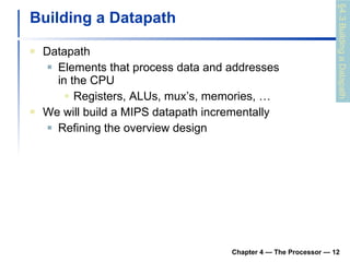
The document summarizes key aspects of CPU and processor design, including:
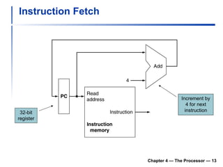
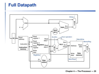
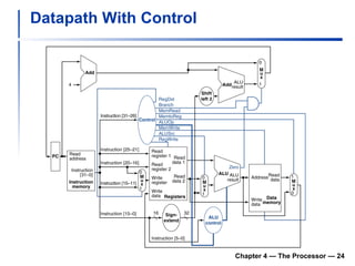
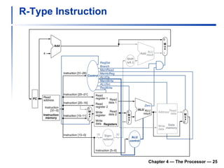
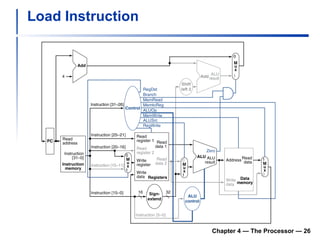
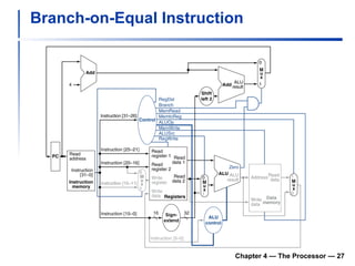
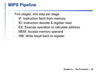
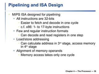
1) It describes the stages of a MIPS pipeline, including instruction fetch, decode, execute, memory access, and write back.
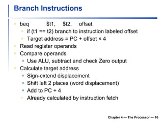
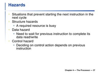
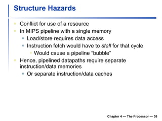
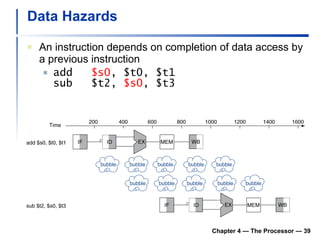
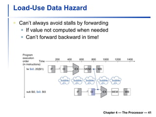
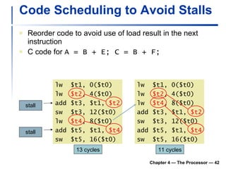
2) It discusses hazards like structure hazards from conflicting resources, data hazards from instructions depending on previous results, and control hazards from branches.
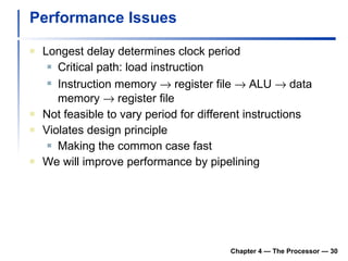
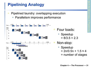
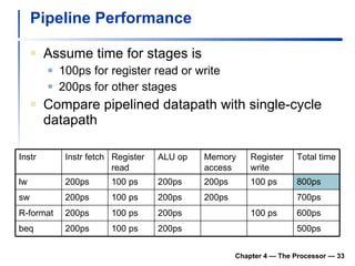
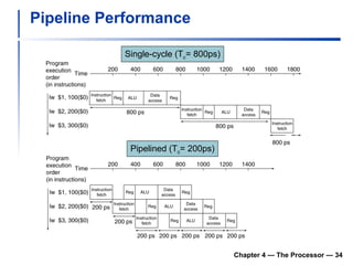
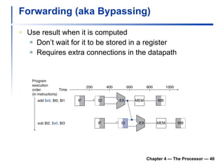
3) Pipelining is introduced to improve performance by overlapping instruction execution, but it requires techniques like forwarding to address hazards between stages.
![Chapter 4 The Processor [Adapted from Computer Organization and Design, 4 th Edition , Patterson & Hennessy, © 2008, MK] [Also adapted from lecture slide by Mary Jane Irwin, www.cse.psu.edu/~mji ]](https://image.slidesharecdn.com/chapter4theprocessor-091015060914-phpapp01/85/Chapter-4-The-Processor-1-320.jpg)
![Chapter 4 The Processor [Adapted from Computer Organization and Design, 4 th Edition , Patterson & Hennessy, © 2008, MK] [Also adapted from lecture slide by Mary Jane Irwin, www.cse.psu.edu/~mji ]](https://image.slidesharecdn.com/chapter4theprocessor-091015060914-phpapp01/75/Chapter-4-The-Processor-1-2048.jpg)
![Clocking Methodology Edge-triggered clocking Combinational logic transforms data during clock cycles between clock edges Input from state elements, output to state element Longest delay determines clock period Chapter 4 — The Processor — [ Edge-triggered clocking ] Of course, the clock cycle must be long enough so that the inputs are stable](https://image.slidesharecdn.com/chapter4theprocessor-091015060914-phpapp01/85/Chapter-4-The-Processor-11-320.jpg)