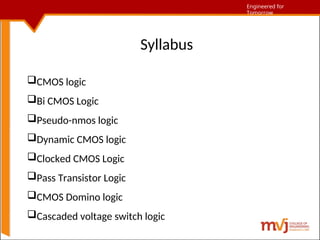
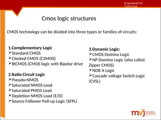
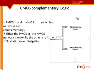
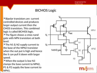
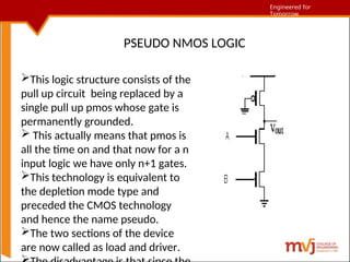
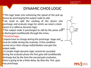
Engineered for Tomorrow
Date : 11/10/14
Prepared by : MN PRAPHUL & ASWINI N
Assistant professor
ECE Department
Engineered for Tomorrow
Subject Name: Fundamentals Of CMOS VLSI
Subject Code: 10EC56
Prepared By: Aswini N, Praphul M N
Department: ECE
Date: 10/11/2014
Engineered for Tomorrow
Engineered for
Tomorrow
Unit 3
Cmos logic structures
Engineered for Tomorrow
Engineered for
Tomorrow
Syllabus
CMOS logic
Bi CMOS Logic
Pseudo-nmos logic
Dynamic CMOS logic
Clocked CMOS Logic
Pass Transistor Logic
CMOS Domino logic
Cascaded voltage switch logic
Engineered for Tomorrow
Engineered for
Tomorrow
Cmos logic structures
CMOS technology can be divided into three types or families of circuits:
1.Complementary Logic
Standard CMOS
Clocked CMOS (C2MOS)
BICMOS (CMOS logic with Bipolar drive
2.Ratio Circuit Logic
Pseudo-NMOS
Saturated NMOS Load
Saturated PMOS Load
Depletion NMOS Load (E/D)
Source Follower Pull-up Logic (SFPL)
3.Dynamic Logic:
CMOS Domino Logic
NP Domino Logic (also called
Zipper CMOS)
NOR A Logic
Cascade voltage Switch Logic
(CVSL)
Engineered for Tomorrow
Engineered for
Tomorrow
CMOS complementary Logic
PMOS and NMOS switching
networks are
complementary .
Either the PMOS or the NMOS
network is on while the other is off.
No static power dissipation.
Engineered for Tomorrow
Engineered for
Tomorrow
BICMOS Logic
Bipolar transistors are current
controlled devices and produces
larger output current then the
CMOS transistors. This combined
logic is called BICMOS logic.
The figure shows a cmos nand
gate with NPN transistors at both
level.
The N1 & N2 supply current to
the base of the NPN2 transistor
when the out put is high and hence
the it can pull it down with larger
speed.
When the output is low N3
clamps the base current to NPN2,
P1 & P2 supply the base current to
NPN1.
Engineered for Tomorrow
Engineered for
Tomorrow
PSEUDO NMOS LOGIC
This logic structure consists of the
pull up circuit being replaced by a
single pull up pmos whose gate is
permanently grounded.
 This actually means that pmos is
all the time on and that now for a n
input logic we have only n+1 gates.
This technology is equivalent to
the depletion mode type and
preceded the CMOS technology
and hence the name pseudo.
The two sections of the device
are now called as load and driver.
Engineered for Tomorrow
Engineered for
Tomorrow
OTHER VARIATIONS OF PSEUDO NMOS
Multi drain logic
One way of implementing pseudo nmos is to use multigrain logic. It represents a
merged transistor kind of implementation. The gates are combined in an open
drain manner, which is useful in some automated circuits
Engineered for Tomorrow
Engineered for
Tomorrow
DYNAMIC CMOS LOGIC
This logic looks into enhancing the speed of the pull up
device by precharging the output node to vdd.
we need to split the working of the device into
precharge and evaluate stage for which we need a clock.
Hence it is called as dynamic logic.
The output node is precharged to vdd by the pmos and
is discharged conditionally through the nmos.
Disadvantages
1.Inputs have to change during the precharge stage and
must be stable during the evaluate. If this condition
cannot occur then charge redistribution corrupts the
output node.
2.A simple single dynamic logic cannot be cascaded.
During the evaluate phase the first gate will conditionally
discharge but by the time the second gate evaluates,
there is going to be a finite delay. By then the first gate
may precharge.
Engineered for Tomorrow
Engineered for
Tomorrow
CMOS DOMINO LOGIC
In this we are able to cascade logic blocks with
the help of a single clock. The precharge and the
evaluate phases retained as they were.
The change required is to add a buffer at the end
of each stage.
This logic works in the following manner. When
the clk=0,ie during the precharge stage the output
of the dynamic logic is high and the output of the
buffer is low.
When the gate is evaluated in the next phase, the
output conditionally goes low and the output of the
buffer goes high.
The advantages are that we can use smaller
gates, achieve higher speed and get a smooth
operation.
Engineered for Tomorrow
Engineered for
Tomorrow
CASCADED VOLTAGE SWITCH
LOGIC(CVSL)
It is a differential kind of logic giving both true and complementary signal
outputs.
The switch logic is used to connect a combinational logic block to a high or a low
output.
There are static and dynamic variants .The dynamic variants use a clock. The
static version (all the figures to shown next) is slower because the pull up devices
have to over come the pull down devices.
Hence the clocked versions with a latching sense amplifier came up. These
switch logic are called sample set differential logic
Engineered for Tomorrow
Engineered for
Tomorrow
STATIC CVSL DYNAMIC CVSL

Dynamic CMOS and Domino logic design .ppt

  • 1.
    Engineered for Tomorrow Date: 11/10/14 Prepared by : MN PRAPHUL & ASWINI N Assistant professor ECE Department Engineered for Tomorrow Subject Name: Fundamentals Of CMOS VLSI Subject Code: 10EC56 Prepared By: Aswini N, Praphul M N Department: ECE Date: 10/11/2014
  • 2.
    Engineered for Tomorrow Engineeredfor Tomorrow Unit 3 Cmos logic structures
  • 3.
    Engineered for Tomorrow Engineeredfor Tomorrow Syllabus CMOS logic Bi CMOS Logic Pseudo-nmos logic Dynamic CMOS logic Clocked CMOS Logic Pass Transistor Logic CMOS Domino logic Cascaded voltage switch logic
  • 4.
    Engineered for Tomorrow Engineeredfor Tomorrow Cmos logic structures CMOS technology can be divided into three types or families of circuits: 1.Complementary Logic Standard CMOS Clocked CMOS (C2MOS) BICMOS (CMOS logic with Bipolar drive 2.Ratio Circuit Logic Pseudo-NMOS Saturated NMOS Load Saturated PMOS Load Depletion NMOS Load (E/D) Source Follower Pull-up Logic (SFPL) 3.Dynamic Logic: CMOS Domino Logic NP Domino Logic (also called Zipper CMOS) NOR A Logic Cascade voltage Switch Logic (CVSL)
  • 5.
    Engineered for Tomorrow Engineeredfor Tomorrow CMOS complementary Logic PMOS and NMOS switching networks are complementary . Either the PMOS or the NMOS network is on while the other is off. No static power dissipation.
  • 6.
    Engineered for Tomorrow Engineeredfor Tomorrow BICMOS Logic Bipolar transistors are current controlled devices and produces larger output current then the CMOS transistors. This combined logic is called BICMOS logic. The figure shows a cmos nand gate with NPN transistors at both level. The N1 & N2 supply current to the base of the NPN2 transistor when the out put is high and hence the it can pull it down with larger speed. When the output is low N3 clamps the base current to NPN2, P1 & P2 supply the base current to NPN1.
  • 7.
    Engineered for Tomorrow Engineeredfor Tomorrow PSEUDO NMOS LOGIC This logic structure consists of the pull up circuit being replaced by a single pull up pmos whose gate is permanently grounded.  This actually means that pmos is all the time on and that now for a n input logic we have only n+1 gates. This technology is equivalent to the depletion mode type and preceded the CMOS technology and hence the name pseudo. The two sections of the device are now called as load and driver.
  • 8.
    Engineered for Tomorrow Engineeredfor Tomorrow OTHER VARIATIONS OF PSEUDO NMOS Multi drain logic One way of implementing pseudo nmos is to use multigrain logic. It represents a merged transistor kind of implementation. The gates are combined in an open drain manner, which is useful in some automated circuits
  • 9.
    Engineered for Tomorrow Engineeredfor Tomorrow DYNAMIC CMOS LOGIC This logic looks into enhancing the speed of the pull up device by precharging the output node to vdd. we need to split the working of the device into precharge and evaluate stage for which we need a clock. Hence it is called as dynamic logic. The output node is precharged to vdd by the pmos and is discharged conditionally through the nmos. Disadvantages 1.Inputs have to change during the precharge stage and must be stable during the evaluate. If this condition cannot occur then charge redistribution corrupts the output node. 2.A simple single dynamic logic cannot be cascaded. During the evaluate phase the first gate will conditionally discharge but by the time the second gate evaluates, there is going to be a finite delay. By then the first gate may precharge.
  • 10.
    Engineered for Tomorrow Engineeredfor Tomorrow CMOS DOMINO LOGIC In this we are able to cascade logic blocks with the help of a single clock. The precharge and the evaluate phases retained as they were. The change required is to add a buffer at the end of each stage. This logic works in the following manner. When the clk=0,ie during the precharge stage the output of the dynamic logic is high and the output of the buffer is low. When the gate is evaluated in the next phase, the output conditionally goes low and the output of the buffer goes high. The advantages are that we can use smaller gates, achieve higher speed and get a smooth operation.
  • 11.
    Engineered for Tomorrow Engineeredfor Tomorrow CASCADED VOLTAGE SWITCH LOGIC(CVSL) It is a differential kind of logic giving both true and complementary signal outputs. The switch logic is used to connect a combinational logic block to a high or a low output. There are static and dynamic variants .The dynamic variants use a clock. The static version (all the figures to shown next) is slower because the pull up devices have to over come the pull down devices. Hence the clocked versions with a latching sense amplifier came up. These switch logic are called sample set differential logic
  • 12.
    Engineered for Tomorrow Engineeredfor Tomorrow STATIC CVSL DYNAMIC CVSL