The document describes the design and implementation of a 64-bit arithmetic logic unit (ALU) for an instruction set architecture. It compares the speed and power consumption of the ALU implemented on different field programmable gate arrays (FPGAs). Key aspects of the ALU design include 16 supported instructions, a power down mode to reduce power consumption when idle, and synthesis for a Spartan2 FPGA using Verilog. Performance metrics like speed, power usage, and resource utilization are reported for the ALU implemented on several FPGAs.
![ISSN: 2278 – 1323
International Journal of Advanced Research in Computer Engineering & Technology
Volume 1, Issue 4, June 2012
FPGA/LUT
FPGA/Slices
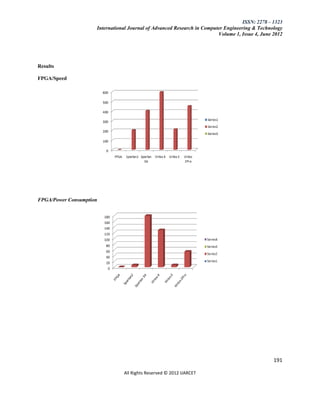
Discussion & Conclusion
The final design is implemented on 0.18µm CMOS Technology with gate count of 36308.Present design is used for
low power consumption. In future we can implement the design for low chip area i.e the low fabrication cost. The
design can be done for high speed but in that case the power consumption increases. So there is a compromise
between the speed & power consumption. The final design supports 203.087 MHz clock frequency when
implemented on FPGA. Virtex 4 provides the highest speed & Spartan 2 provides the lowest power consumption.
Virtex 4 Provides low chip area (slices are less).Among these architectures Virtex E provides high speed and low
power consumption.
References
[1]L.Benini, G.D., Micheli, “Dynamic Power Management,” 1st ed.Springer, Nov 1997, pp.24-25
[2]Steve Furber, ARM: System on Chip Architecture, Addison –Wesley, second edition, 2000.
[3]D.A Patterson & J.L Henessey, Computer Architecture: A Quantative Approach, Sant Mateo,
192
All Rights Reserved © 2012 IJARCET](https://image.slidesharecdn.com/186-193-120630093840-phpapp01/85/186-193-7-320.jpg)
![ISSN: 2278 – 1323
International Journal of Advanced Research in Computer Engineering & Technology
Volume 1, Issue 4, June 2012
CA: Morgan Kaufman, 1989.
[4] Dr.R.S Ramchandran, “Digital VLSI System Design”, IIT Madras
[5]Computer Architecture & Parallel Processing, Kai Hwang
[6]Rajeev Kumar, “Design of 64bit Register File for VLIW Processor Architecture”, IJERA vol.2,
issue.3, May-June 2012, pp.183-186.
Rajeev Kumar obtained his MSc Electronic Science & M.Tech (Microelectronics & VLSI Design) Degree from
Deptt of Electronic Science, Kurukshetra University, Kurukshetra (Haryana).Currently working as Coordinator
M.Tech ECE Program in IITT College of Engineering, Punjab. He is the member of R&D in the IITT College. He is
also the member of IAENG (International Association of Engineers), Research Gates & Silicon India. He worked in
the field of High Speed Processor Architecture, Low Power VLSI Design & Implementation of Hardware for DSP.
He is currently involved in Design & Implementation of VLIW Processor for Reconfigurable Architecture. In future
he is interested to work in ASIP Design for Low Power, Design of Hardware for Neural Network and Design of
DSP Processor for Image Processing. He is keen for Reconfigurable Computing. During M.Tech they are involved
in Full Custom design of 0.1µm NMOS inverter. For Synthesis purpose in Verilog HDL based design they used the
library of Semi Custom Design (ASIC) & FPGA. He is involved logic verification of gates & architecture in C
Language in Linux Operating System. They worked in the area of Microelectronics during MSc Electronic Science
(Thin Film Deposition, Photolithography & Wet Etching).
Manpreet Kaur done his B.Tech ECE from Bhutta College of Engineering Ludhiana, Punjab.Pursuing M.Tech ECE
form IITT College of Engineering,Punjab.In B.Tech they done their project in Dynamic Host Configuration.Her
research interest is DSP, Wireless & Mobile Communication, and Low Power VLSI Design. In future she is
interested to work in high performance Reconfigurable Computing.
193
All Rights Reserved © 2012 IJARCET](https://image.slidesharecdn.com/186-193-120630093840-phpapp01/85/186-193-8-320.jpg)