Downloaded 147 times
![Pardeep Kumar, Susmita Mishra, Amrita Singh / International Journal of Engineering
Research and Applications (IJERA) ISSN: 2248-9622 www.ijera.com
Vol. 3, Issue 3, May-Jun 2013, pp.509-513
510 | P a g e
A+B+Cin=2xCout +Sum (1)
The conventional logic equation for Sum and Carry
are:
Cout= (A∙B) + (A+B)∙Cin (2)
Sum= (A∙B∙Cin) + (A+B+Cin) ∙Cout (3)
By modifying the equations (2) and (3) the
following logics were proposed:-
Sum= A B Cin (4)
Cout= Cin (A B) +A∙(A B) (5)
Sum= A B Cin (6)
Sum= (Cin∙(A B)) + (Cin∙(A B) (7)
Cout= Cin (A∙B) + Cin∙(A+B) (8)
Full Adder using CMOS Logic and will be called as
“Conventional CMOS design”.
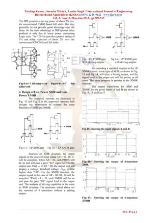
3. Existing full adder circuits
There are standard implementations for the
full-adder cell that are used from last few years
some of them among these adders there are the
following:-
Figure.1- The Conventional CMOS full-adder
The CMOS full adder (CMOS)[1] has 28 transistors
and is based on the regular CMOS structure
The Mirror logic [6] style based full adder has 28
transistors
Figure-2: Mirror logic style based full adder
The DPL logic [3] style based full adder has 28
transistors
A Transmission gate full adder [4] using 18
transistors
A full adder cell using 14 transistors
A full adder cell using 10 transistors
Figure: 3-DPL logic style based full adder
Figure-4: Transmission gate full adder](https://image.slidesharecdn.com/ch33509513-130523022956-phpapp01/85/Ch33509513-2-320.jpg)
![Pardeep Kumar, Susmita Mishra, Amrita Singh / International Journal of Engineering
Research and Applications (IJERA) ISSN: 2248-9622 www.ijera.com
Vol. 3, Issue 3, May-Jun 2013, pp.509-513
513 | P a g e
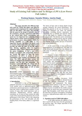
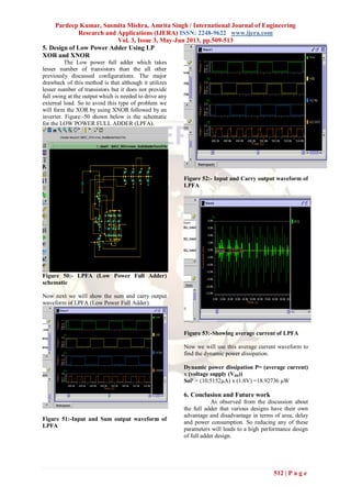
Hence we can see that LPFA (Low Power Full
Adder) is better than all the other full adder designs
in terms of Power consumption, Area (Number of
Transistor), Delay, PDP (Power Delay Product.
Future work will be focused on the
reduction of any of the parameter shown above i.e.
Area, Delay and Power. There is also another term
i.e. PDP (power delay product) this is generally
used for to make a trade-off between power
consumption and delay.
Table 5:- Showing the comparison of
performance Conventional CMOS full Adder,
BBL-PT based full adder, HYBRID FULL
ADDER and LPFA
Desig
n
Del
ay(
ps)
Static
Power
Dissipa
tion(p
W)
Dynam
ic
Power
Dissipa
tion(µ
W)
Tota
l
Pow
er(µ
W)
Tra
nsist
or
Cou
nt
Conv
entio
nal
CMO
S full
adder
124 143.59
2
23.744
3
23.74
443
28
BBL-
PT
logic
based
full
adder
110.
3 126.30
8
22.606
38
22.60
6506
27
Hybri
d full
adder
142 158.67
4
29.787
1
29.78
7258
30
Low
Powe
r full
adder
(LPF
A)
101.
2
113.86
9
18.927
36
18.92
7473
26
Figure-5
References
[1]. I.Hassoune, A.Neve, J.Legat, and
D.Flandre, “Investigation of low-power
circuit techniques for a hybrid full-adder
cell,” in Proc. PATMOS 2004, pp. 189–
197, Springer-Verlag
[2]. A.M.Shams, Tarek k.darwish,”
performance analysis of low-power 1-bit
CMOS full adder cells IEEE Trans. Very
Large Scale Integ. (VLSI) Syst vol. 10 no
.1, pp.20-29, feb.2002.
[3]. C.-H. Chang, M. Zhang, “A review of
0.18 m full adder performances for tree
structured arithmetic circuits,” I EEE
Trans. Very Large Scale Integration.
(VLSI) Syst. vol. 13, no. 6, pp. 686–694,
Jun. 2005.
[4]. M.aguir re, M.linares “an alternative
logic app roach to implement high speed
low power full adder cells”SBBCI SEP
2005 PP. 166-171.
[5] A.K. Aggarwal, S. wairya, and
S.Tiwari,”a new full adder for high
speed low power digital circuits “world
science of journal 7 special issue of
computer and IT: June 2009,pp.- 138-144.
[6] M.Hossein, R.F.Mirzaee, K.Navi and
T.Nikoubin” new high performance
majority function based full adder cell” 14
inter national CSI conference 2009, pp.
100- 104.
[7] A.M.Shams,” A new full adder cell for
low power applications“ centre for
advance computer studies, university of
southwestern Louisiana.
[8] D.Radhakrishnan,” low power CMOS full
adder” IEE proc: - circuits devices system
vol. 148 no. 1 Feb. 2001.pp- 19-24.
[9] John p. Uyemura “Introduction to VLSI
circuits and systems”](https://image.slidesharecdn.com/ch33509513-130523022956-phpapp01/85/Ch33509513-5-320.jpg)

The paper reviews various CMOS full adder designs, focusing on their power consumption, speed, and area, while proposing a new low power full adder (LPFA) that improves upon these parameters. The authors highlight the conflict between power efficiency and speed, emphasizing the importance of the power delay product (PDP) as a performance metric. Simulations of the LPFA demonstrate advantages in power consumption, transistor count, and delay when compared to conventional full adder designs.


![[IJCT-V3I2P23] Authors: Baljinder Kaur, Narinder Sharma](https://cdn.slidesharecdn.com/ss_thumbnails/ijct-v3i2p23-160609062619-thumbnail.jpg?width=640&height=640&fit=bounds)