Downloaded 24 times

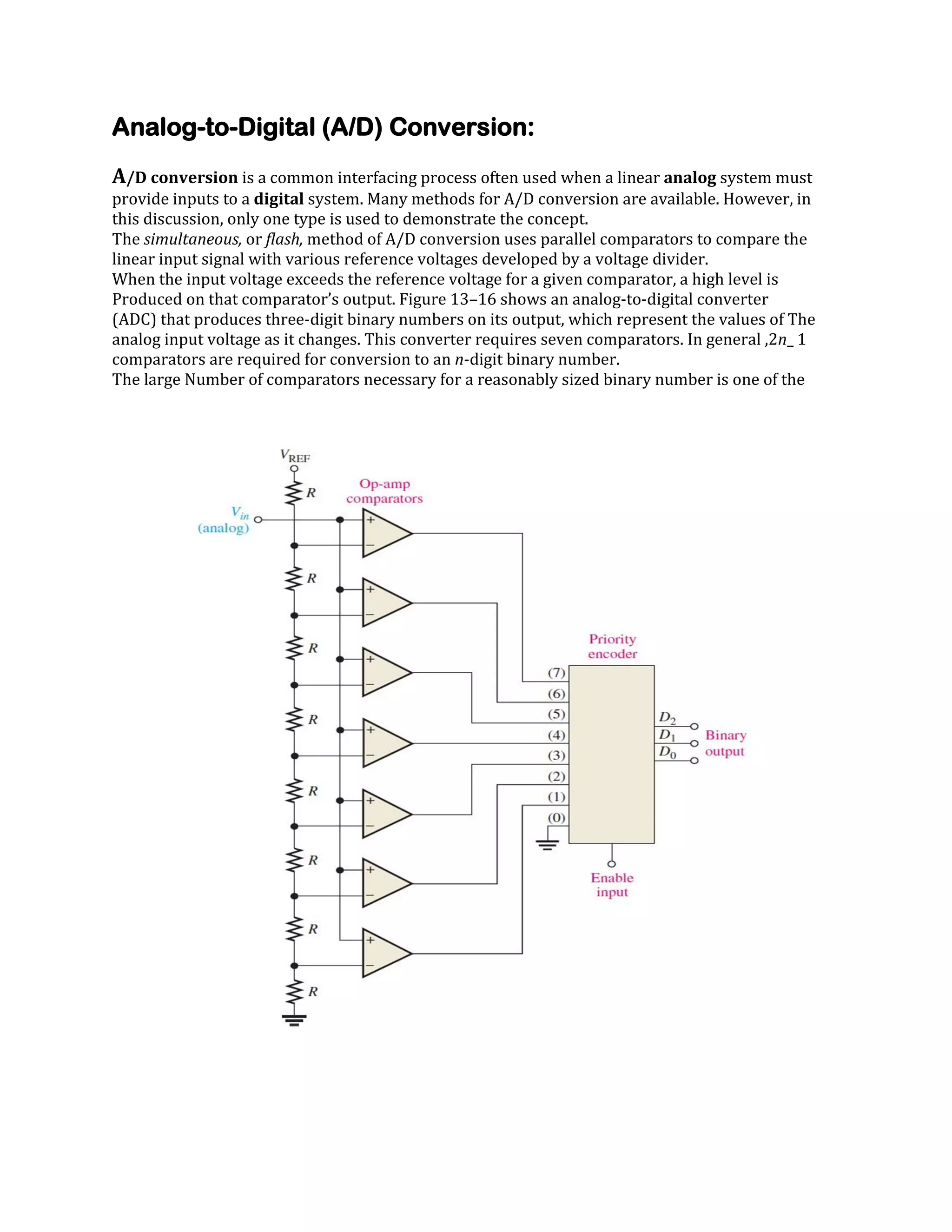
![Light Sensor LDR [light depended resistor]:
A Photoconductive light sensor does not produce electricity but simply changes its physical
properties when subjected to light energy. The most common type of photoconductive
device is the Photo resistor which changes its electrical resistance in response to changes
in the light intensity. Photo resistors are Semiconductor devices that use light energy to
control the flow of electrons, and hence the current flowing through them. The commonly
used Photoconductive Cell is called the Light Dependent Resistor or LDR.
As its name implies, the Light Dependent Resistor (LDR) is made from a piece of exposed
semiconductor material such as cadmium sulphide that changes its electrical resistance
from several thousand Ohms in the dark to only a few hundred Ohms when light falls upon
it by creating hole-electron pairs in the material.
The net effect is an improvement in its conductivity with a decrease in resistance for an
increase in illumination. Also, photo resistive cells have a long response time requiring
many seconds to respond to a change in the light intensity.](https://image.slidesharecdn.com/ieprojectreport-140127160025-phpapp02/75/Project-Report-9-2048.jpg)
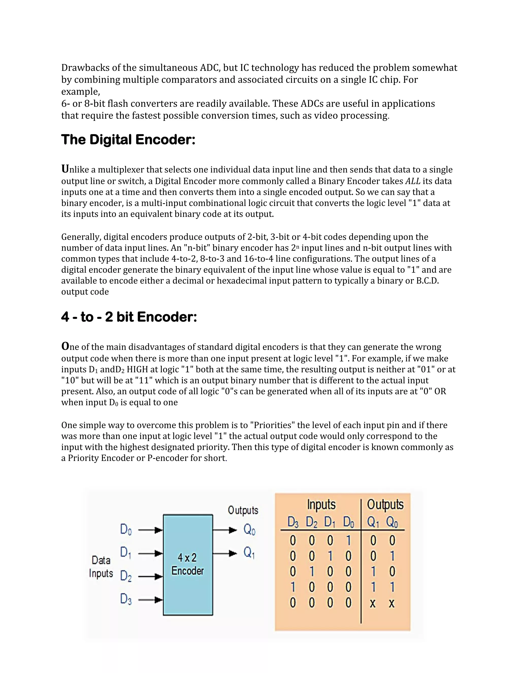
![8 - to - 4 bit Encoder or [Priority Encoder]:
The Priority Encoder solves the problems mentioned above by allocating a priority level to each
input. The priority encoders output corresponds to the currently active input which has the highest
priority. So when an input with a higher priority is present, all other inputs with a lower priority
will be ignored. The priority encoder comes in many different forms with an example of an 8-input
priority encoder along with its truth table shown below.
Priority encoders are available in standard IC form and the TTL 74LS148 is an 8-to-3 bit priority
encoder which has eight active LOW (logic "0") inputs and provides a 3-bit code of the highest
ranked input at its output. Priority encoders output the highest order input first for example, if
input lines "D2", "D3" and "D5" are applied simultaneously the output code would be for input "D5"
("101") as this has the highest order out of the 3 inputs. Once input "D5" had been removed the
next highest output code would be for input "D3" ("011"), and so on](https://image.slidesharecdn.com/ieprojectreport-140127160025-phpapp02/75/Project-Report-13-2048.jpg)
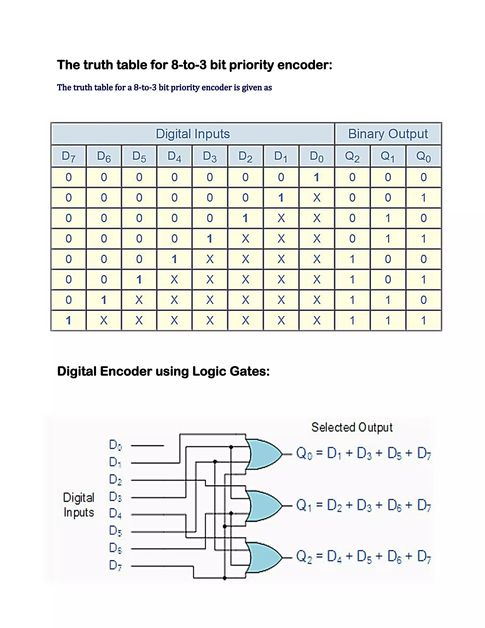
![Datasheet of74LS147 [priority encoder]:
(a) internal logic diagram of 74LS147
(b) pin out of 74LS14or 74148
© recommended operating conditions
(Dip) dual inline package dimensions of 74LS147 or 74LS1478](https://image.slidesharecdn.com/ieprojectreport-140127160025-phpapp02/75/Project-Report-15-2048.jpg)
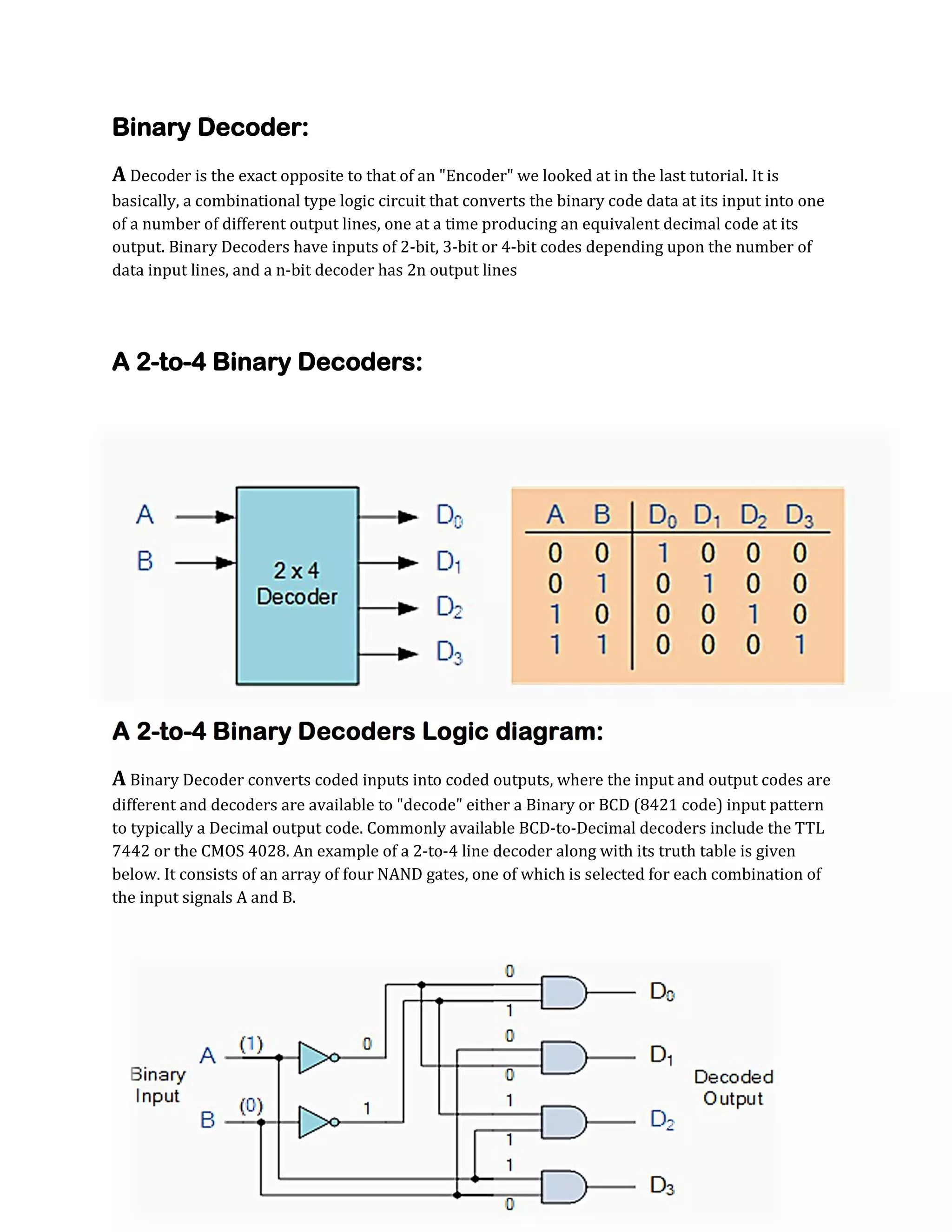
![Datasheet for 7-segment decoder [74LS47 or 74LS48]:
(A)Internal logic diagram for 74LS48
(b) Pin out for 74LS48 or74LS47
© recommended operating conditions](https://image.slidesharecdn.com/ieprojectreport-140127160025-phpapp02/75/Project-Report-20-2048.jpg)
![PCB [Printed circuit board]layout:
(a)
Bottom view(b)
silk layer](https://image.slidesharecdn.com/ieprojectreport-140127160025-phpapp02/75/Project-Report-23-2048.jpg)
![PCB [Printed circuit board] Making Process Step by Step….
Step 1: Prepare a layout of the circuit on any commonly used PCB designing software. A layout is a
design which interconnects the components according to the schematic diagram (circuit diagram).
Take a mirror image print of the layout on the OHP sheet using a laser printer. Make sure that the
design is correct with proper placement of the components.
Step 2: Cut the copper board according to the size of layout. A copper board is the base of a PCB, it
can be single layer, double layer or multi-layer board.
Single layer copper board has copper on one side of the PCB, they are used to make single layer
PCBs, it is widely used by hobbyist or in the small circuits. A double layer copper board consists of
copper on both the sides of the PCB. These boards are generally used by the industries. A multilayer
board has multiple layers of copper; they are quite costly and mainly used for complex circuitries
like mother board of PC.
Step 3: Rub the copper side of PCB using steel wool. This removes the top oxide layer of copper as
well as the photo resists layer if any.
Step 4: Place the OHP sheet (wax paper) which has the printed layout on the PCB sheet. Make sure
that the printed/mirror side should be placed on the copper side of PCB
Step 5: Put a white paper on the OHP sheet and start ironing. The heat applied by the electric iron
causes the ink of the traces on the OHP sheet to stick on the copper plate exactly in the same way it
is printed on the OHP sheet. This means that the copper sheet will now have the layout of the PCB
printed on it. Allow the PCB plate to cool down and slowly remove the OHP sheet. Since it is manual
process it may happen that the layout doesn’t comes properly on PCB or some of the tracks are
broken in between. Use the permanent marker and complete the tracks properly.
Step 6: Now the layout is printed on PCB. The area covered by ink is known as the masked area and
the unwanted copper, not covered by the ink is known as unmasked area. Now make a solution of
ferric chloride. Take a plastic box and fill it up with some water. Dissolve 2-3 tea spoon of ferric
chloride power in the water. Dip the PCB into the Etching solution (Ferric chloride solution, Fecl3)
for approximately 30 mins. The Fecl3 reacts with the unmasked copper and removes the unwanted
copper from the PCB. This process is called as Etching. Use pliers to take out the PCB and check if
the entire unmasked area has been etched or not. In case it is not etched leave it for some more
time in the solution
Step 7: Take out the PCB wash it in cold water and remove the ink by rubbing it with steel wool.
The remaining area which has not been etched is the conductive copper tracks which connect the
components as per the circuit diagram.
Step 8: Now carefully drill the PCB using a drilling machine on the pads
Step 9: Put the components in the correct holes and solder them.](https://image.slidesharecdn.com/ieprojectreport-140127160025-phpapp02/75/Project-Report-24-2048.jpg)

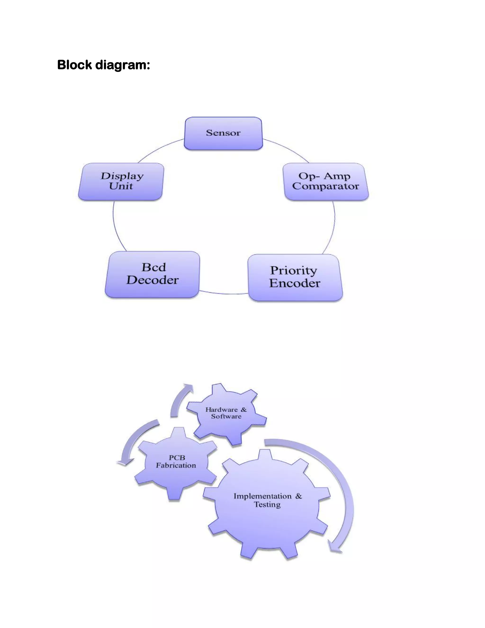
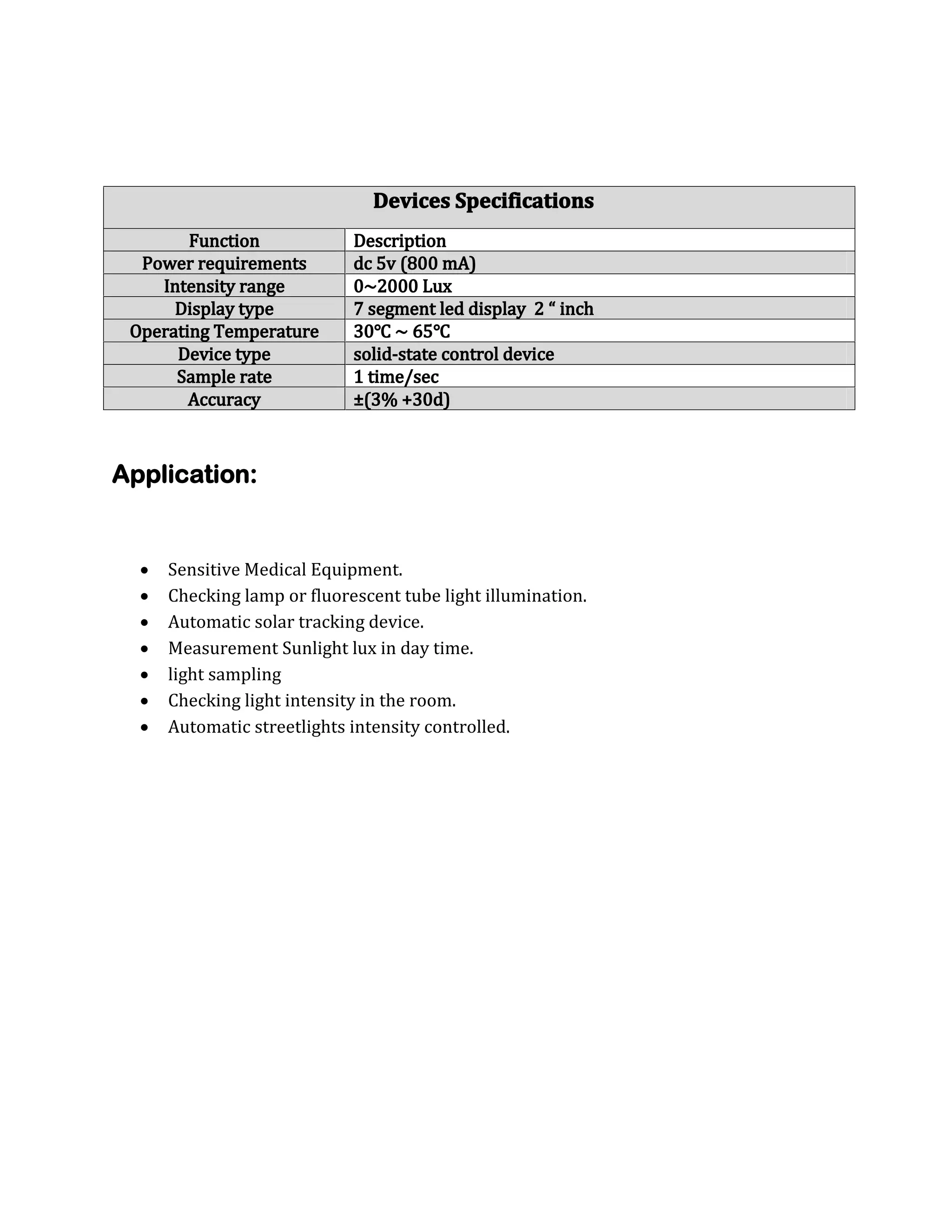
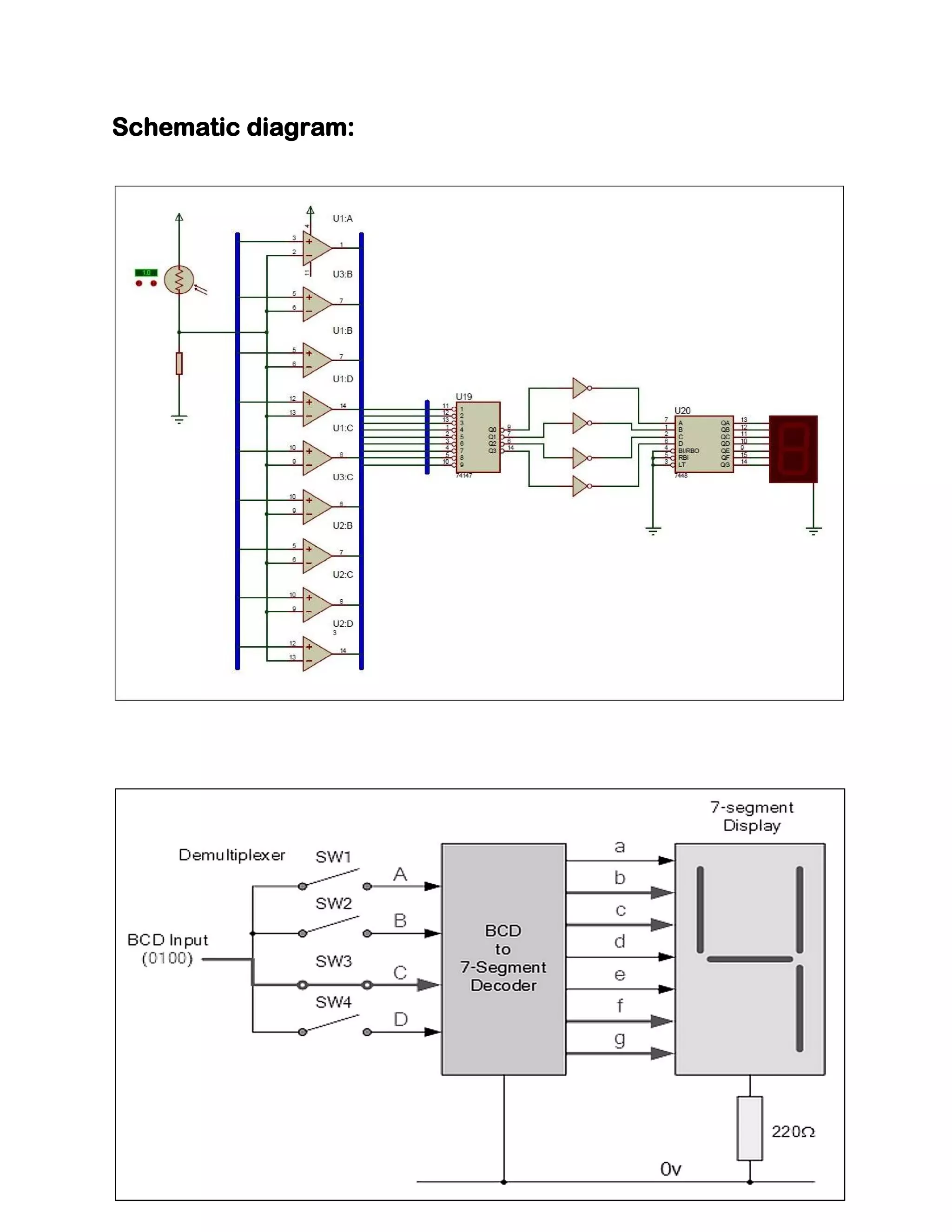
This document describes the design and development of a light intensity meter circuit. The circuit uses a light dependent resistor, voltage divider network, operational amplifiers, analog to digital conversion, and a priority encoder to measure light levels. The output is displayed on a 7-segment display. Key components include an LM324 op-amp, LDR light sensor, 74LS147 priority encoder, and 74LS48 BCD to 7-segment decoder. The circuit aims to provide an inexpensive and accurate way to measure light intensity with a range of 0-2000 lux.