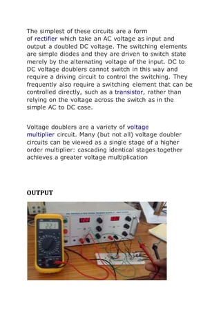
SREENIDHI INSTITUTE OF SCIENCE AND 
TECHNOLOGY 
LINEAR AND DIGITAL IC APPLICATIONS LAB 
PROJECT ON VOLTAGE DOUBLER 
B.TECH 3/4 YEAR SEMESTER-1 
EEE 
BY 
K.KRISHNAVENI (12311A0227) 
K.KARTHIK (12311A0226) 
K.KAPIL (12311A0225)
VOLTAGE DOUBLER 
Most of this project is circuit used for doubling the 
voltage uses the principle of charging and discharging 
the capacitor. The voltage doubler circuit described 
below is used to double the input DC power by using 
IC 555 timer with capacitors and diodes. This circuit is 
useful when higher voltage level is required from a 
single lower voltage power supply. 
This voltage doubler project is based on 555 timer 
wired in astable mode means it will produce a square 
wave at a frequency of 2KHz approx with the help of 
components R1,R2 and C1.When input power is 
supplied to the circuit an output is produced at PIN3 of 
IC1. 
This dc voltage doubler circuit produces a voltage that 
is twice its voltage supply. This is useful when a higher 
voltage level is needed out of a single lower voltage 
power supply. Since the current consumption levels are 
low in such cases, the circuit can be built with minimal 
resources.
Voltage Doubler Circuit Schematic 
The electronic circuit is basically a square wave 
generator using the common LM555 timer IC. It is 
followed by a final stage made of transistors T1 and T2. 
The actual doubler circuit is made of D1, D2, C4 and C5 
components. 
The 555 dc voltage doubler timer IC works as an 
astable multivibrator and generates a frequency of 
about 8.5 kHz. The quare wave output drives the final 
stage made of T1 and T2. This is how the doubler 
works: by a low amplitude of the signal, transistor T1 
blocks while T2 conducts. The minus electrode of the 
capacitor C4 is grounded and charges through D1. By a 
high amplitude of the signal, transistor T1 conducts 
while T2 blocks. However, capacitor C4 cannot 
discharge because it is blocked by D1. The following 
capacitor C5 is therefore charged with a combined 
voltage from C4 and the power supply (12V input).
On standby, the circuit delivers around 20 volts. The 
maximum load must not exceed 70 mA. The actual 
output voltage is around 18 volts giving an efficiency 
rating of 32 %. 
On lower current ratings, the voltage is higher. 
If a stable voltage lever is desired, a 3 pin voltage 
regulator IC can be added at the output. The regulator 
IC’s own current consumption must be added to the 
total current consumption which must not exceed 70 
mA. 
A voltage doubler is an electronic circuit which 
charges capacitors from the input voltage and switches 
these charges in such a way that, in the ideal case, 
exactly twice the voltage is produced at the output as 
at its input.
The simplest of these circuits are a form 
of rectifier which take an AC voltage as input and 
output a doubled DC voltage. The switching elements 
are simple diodes and they are driven to switch state 
merely by the alternating voltage of the input. DC to 
DC voltage doublers cannot switch in this way and 
require a driving circuit to control the switching. They 
frequently also require a switching element that can be 
controlled directly, such as a transistor, rather than 
relying on the voltage across the switch as in the 
simple AC to DC case. 
Voltage doublers are a variety of voltage 
multiplier circuit. Many (but not all) voltage doubler 
circuits can be viewed as a single stage of a higher 
order multiplier: cascading identical stages together 
achieves a greater voltage multiplication 
OUTPUT
APPLICATIONS 
 A doubler can increase a low voltage to a very high 
voltage by adding stages the application is study of 
high voltage behavior to plasma study to 
entertainment of globe arcing to ions generators to 
eliminate odors. 
 voltage-doubler in rectifying LLC multi-resonant 
converter. 
 Voltage doubler is also used in isolated resonant 
converters. 
 It is used to produce a voltage that is twice its 
voltage supply.

Voltagedoubler

  • 1.
    SREENIDHI INSTITUTE OFSCIENCE AND TECHNOLOGY LINEAR AND DIGITAL IC APPLICATIONS LAB PROJECT ON VOLTAGE DOUBLER B.TECH 3/4 YEAR SEMESTER-1 EEE BY K.KRISHNAVENI (12311A0227) K.KARTHIK (12311A0226) K.KAPIL (12311A0225)
  • 2.
    VOLTAGE DOUBLER Mostof this project is circuit used for doubling the voltage uses the principle of charging and discharging the capacitor. The voltage doubler circuit described below is used to double the input DC power by using IC 555 timer with capacitors and diodes. This circuit is useful when higher voltage level is required from a single lower voltage power supply. This voltage doubler project is based on 555 timer wired in astable mode means it will produce a square wave at a frequency of 2KHz approx with the help of components R1,R2 and C1.When input power is supplied to the circuit an output is produced at PIN3 of IC1. This dc voltage doubler circuit produces a voltage that is twice its voltage supply. This is useful when a higher voltage level is needed out of a single lower voltage power supply. Since the current consumption levels are low in such cases, the circuit can be built with minimal resources.
  • 3.
    Voltage Doubler CircuitSchematic The electronic circuit is basically a square wave generator using the common LM555 timer IC. It is followed by a final stage made of transistors T1 and T2. The actual doubler circuit is made of D1, D2, C4 and C5 components. The 555 dc voltage doubler timer IC works as an astable multivibrator and generates a frequency of about 8.5 kHz. The quare wave output drives the final stage made of T1 and T2. This is how the doubler works: by a low amplitude of the signal, transistor T1 blocks while T2 conducts. The minus electrode of the capacitor C4 is grounded and charges through D1. By a high amplitude of the signal, transistor T1 conducts while T2 blocks. However, capacitor C4 cannot discharge because it is blocked by D1. The following capacitor C5 is therefore charged with a combined voltage from C4 and the power supply (12V input).
  • 4.
    On standby, thecircuit delivers around 20 volts. The maximum load must not exceed 70 mA. The actual output voltage is around 18 volts giving an efficiency rating of 32 %. On lower current ratings, the voltage is higher. If a stable voltage lever is desired, a 3 pin voltage regulator IC can be added at the output. The regulator IC’s own current consumption must be added to the total current consumption which must not exceed 70 mA. A voltage doubler is an electronic circuit which charges capacitors from the input voltage and switches these charges in such a way that, in the ideal case, exactly twice the voltage is produced at the output as at its input.
  • 5.
    The simplest ofthese circuits are a form of rectifier which take an AC voltage as input and output a doubled DC voltage. The switching elements are simple diodes and they are driven to switch state merely by the alternating voltage of the input. DC to DC voltage doublers cannot switch in this way and require a driving circuit to control the switching. They frequently also require a switching element that can be controlled directly, such as a transistor, rather than relying on the voltage across the switch as in the simple AC to DC case. Voltage doublers are a variety of voltage multiplier circuit. Many (but not all) voltage doubler circuits can be viewed as a single stage of a higher order multiplier: cascading identical stages together achieves a greater voltage multiplication OUTPUT
  • 6.
    APPLICATIONS  Adoubler can increase a low voltage to a very high voltage by adding stages the application is study of high voltage behavior to plasma study to entertainment of globe arcing to ions generators to eliminate odors.  voltage-doubler in rectifying LLC multi-resonant converter.  Voltage doubler is also used in isolated resonant converters.  It is used to produce a voltage that is twice its voltage supply.