SlideShare a Scribd company logo
1 of 25
Download to read offline
Department of Electronics and Telecommunication Engineering
Mini project Title: Voltage Doubler
Circuit using 555 Timer IC
11-10-2023
1/total slides
Name & Roll no:
• 352 Bhushan Sawant
• 353 Bharat Yadav
• 360 Afzal Shaikh
• 371 Rishabh Vishwakarma
Under Guidance of
Prof. M.K.Ahirrao
Department of Electronics and Telecommunication Engineering
Outline of the Presentation
Introduction
Background
Circuit Design
Testing and Results
Results and Conclusion
2
Introduction Background Circuit Design Testing and Results Conclusions
Department of Electronics and Telecommunication Engineering
Introduction
• Motivation
• Background
• Block diagram
3
Background Circuit Design Testing and Results Conclusions
Introduction
Department of Electronics and Telecommunication Engineering
Motivation
• The motivation for creating a voltage doubler circuit using a 555 timer IC
lies in the educational value, practical applications, and the opportunity for
hands-on learning and experimentation in the field of electronics. This
project can serve as an exciting and informative way to enhance your
electronics knowledge and skills.
4
Background Circuit Design Testing and Results Conclusions
Introduction
Department of Electronics and Telecommunication Engineering
Background
• This project offers an opportunity to learn and gain practical experience in
electronics. It involves understanding the functioning of the 555 timer IC, diodes,
capacitors, and voltage doubling principles, which are fundamental in electronics
5
Background Circuit Design Testing and Results Conclusions
Introduction
Department of Electronics and Telecommunication Engineering
Block Diagram
6
Background Circuit Design Testing and Results Conclusions
Introduction
5
5
5
Timer
IC
Power supply
(5v)
Resistors
Capacitors
1N4007
Diode
Multimeter
/Voltmeter
Department of Electronics and Telecommunication Engineering
Background
• Concepts
• History
7
Circuit Design Testing and Results Conclusions
Introduction Background
Department of Electronics and Telecommunication Engineering
Concepts
The capacitor allows AC current to pass through it, but the diode only allows current to flow in
one direction. This creates a peak output voltage of 2*V pk across the diode. This extremely
simple circuit illustrates the concept, but it does not regulate the output DC voltage very well
8
Circuit Design Testing and Results Conclusions
Introduction Background
Department of Electronics and Telecommunication Engineering
History
Greinacher circuit
The Greinacher voltage doubler is a significant improvement over the Villard circuit for a small cost in additional
components. The ripple is much reduced, nominally zero under open-circuit load conditions, but when current is
being drawn depends on the resistance of the load and the value of the capacitors used. The circuit works by
following a Villard cell stage with what is in essence a peak detector or envelope detector stage. The peak detector
cell has the effect of removing most of the ripple while preserving the peak voltage at the output. The Greinacher
circuit is also commonly known as the half-wave voltage doubler.
9
Circuit Design Testing and Results Conclusions
Introduction Background
Department of Electronics and Telecommunication Engineering
Circuit Design & Working
• Circuit Interfacing Diagram.
• Working
• Main components and their specifications and principle of operation.
• Applications.
10
Testing & Results Conclusions
Introduction Background Circuit Design
Department of Electronics and Telecommunication Engineering
Circuit Interfacing Diagram.
11
Testing & Results Conclusions
Introduction Background Circuit Design
Department of Electronics and Telecommunication Engineering
Working
12
Testing & Results Conclusions
Introduction Background Circuit Design
• A voltage doubler circuit using a 555 timer IC is an electronic circuit that takes an input voltage
and produces an output voltage that is approximately double the input voltage. The circuit
operates by generating an oscillating square wave signal using the 555 timer in its astable mode
and then using diodes and capacitors to double the voltage
Department of Electronics and Telecommunication Engineering
Components
• 555 Timer IC
• 1N4007 Diode -2
• Resistors 10K
• Resistor 33K
• Capacitor 22uF – 2
• Capacitor 0.01uF – 2
• 3V-12V Battery
13
Testing & Results Conclusions
Introduction Background Circuit Design
Department of Electronics and Telecommunication Engineering
Components specifications
555 Timer IC :
• In astable mode, the 555 timer IC generates a continuous square wave output with a specific
frequency and duty cycle. The frequency and duty cycle are determined by the resistors R1 and
R2 and capacitor C1 connected to pins 2, 6, and 7 of the IC.
• 1N4007 Diode :
• 1N4007 rectifier diode has in total 2 pins, owns a cathode (-) and anode (+). In the schematic
symbol, the tip of the triangle with the line on top of it is the cathode. The cathode is marked on
the body of a diode by a band. It allows current flow through only one direction that means the
anode to the cathode only and never from the cathode to the anode – it likes a one current can
flow from way value.
14
Testing & Results Conclusions
Introduction Background Circuit Design
Department of Electronics and Telecommunication Engineering
• Resistors:
• A resistor is the most basic electronic component invariably found almost every electronic
circuit. It is a passive element. The most important function of resistor is to resist the flow of
current. The property of a resistor is known as resistance.
• Capacitor:
• It provides the value of a capacitor C as farads moreover printed or color coded over the body of
the capacitor. Its units are Farads. Practical capacitors are available from 1pf to 1000 mF.
15
Testing & Results Conclusions
Introduction Background Circuit Design
Department of Electronics and Telecommunication Engineering
Applications
• Low-power Devices
• LED Drivers
• Photoflash Units
• LCD Displays
• RF Transmitters
• Lab Experiments and Prototyping
16
Testing & Results Conclusions
Introduction Background Circuit Design
Department of Electronics and Telecommunication Engineering
Testing & Results
This circuit's operation is the switching action of the diodes and the energy transfer between the
capacitors during each cycle of the 555 timer's square wave signal. By continuously repeating this
process, the circuit effectively doubles the input voltage, making it useful in various applications
where a higher voltage is required from a lower voltage power source.
17
Introduction Background Circuit Design Conclusions
Testing and Results
Department of Electronics and Telecommunication Engineering
Testing
18
Introduction Background Circuit Design Conclusions
Testing and Results
Department of Electronics and Telecommunication Engineering
Result
19
Introduction Background Circuit Design Conclusions
Testing and Results
Department of Electronics and Telecommunication Engineering
Conclusion
• Summary
• Future Works
• Precautions
20
Introduction Background Circuit Design Testing and Results Conclusions
Department of Electronics and Telecommunication Engineering
Summary
• The circuit is the one which doubles the voltage and consists of 2 capacitors and 2 diodes connected in the manner
shown in the circuit diagram. The 555-timer has multiple modes in which we have decided today to use astable
Multivibrator mode. This mode can be used to generate a square wave of approximately 2KHz using a
combination of two resistors and a capacitor. From the circuit, we can see that when the pin 3 of the timer IC has a
low output, then the diode D1 gets forward biased, which will charge capacitor C3 through it.
• Because the capacitor is charged directly from the supply, the capacitor will also get charged to the voltage equal
to the input voltage. When the pulse from the timer IC is high, the pin 3 of the IC will show a high output. This
will make the diode D1 reversed biased, and this blocks the charging of the capacitor C3 which has now been
charged to approximately the voltage equal to the supply voltage.
• When the diode D1 is reversed biased, the diode D2 will be forward biased, and this will charge the capacitor C4
through it. C4 capacitor will also be charge with the energy stored in capacitor C3. Now the capacitor C4 has
double the voltage of the input voltage because it is charged via two paths one from the capacitor C3 which was
charged initially to the supply voltage and another path is directly through the supply.
• In theory, the output of this circuit must produce a voltage at the output equal to double the voltage at the input, but
in reality, the charging and discharging of a capacitor is not a lossless process, the energy stored in a capacitor is
not fully transmitted to the other capacitor, and the charging of the capacitor is also not ideal.
21
Introduction Background Circuit Desing Testing and Results Conclusions
Department of Electronics and Telecommunication Engineering
Further Improvements
• We can cascade the diode-capacitor arrangement at the output of 555 timer IC to generate much
higher voltages. The resulting circuit is called as a voltage multiplier circuit. It outputs a certain
times input voltage as output voltage. The factor by which the output voltage is more than the
input voltage is determined by the number of stages of capacitor+diode charge pump blocks
used
22
Introduction Background Circuit Working Testing and Results Conclusions
Department of Electronics and Telecommunication Engineering
Precautions
• Due to the limitations of the timer IC, the input voltage of the circuit cannot be greater than 12V
and less than 3V, choosing a voltage between 3 and 12V will ensure safe working and no
damage will be done to the components.
• As discussed above, the working of the circuit depends on the charging and discharging of
capacitors, and hence, the circuit will not give output of required value right away as soon as the
circuit is plugged in with a supply voltage, but it will take a while before it settles at double the
input voltage.
23
Introduction Background Circuit Working Testing and Results Conclusions
Department of Electronics and Telecommunication Engineering
Thank You
24
Department of Electronics and Telecommunication Engineering
References
• https://how2electronics.com/voltage-doubler-circuit-using-555-
timer-ic/
25

More Related Content

Similar to voltage doubler using 555 timer ic

Final esd lab manual (1)
Final esd lab manual (1)Final esd lab manual (1)
Final esd lab manual (1)Deepak Jena
 
Report on minor project
Report on minor projectReport on minor project
Report on minor projectAnil Maurya
 
Report on PCB designing and fabrication by Prince Rohan
Report on PCB designing and fabrication by Prince RohanReport on PCB designing and fabrication by Prince Rohan
Report on PCB designing and fabrication by Prince RohanRohan Das
 
DIODE APPLICATIONS .pdf
DIODE APPLICATIONS .pdfDIODE APPLICATIONS .pdf
DIODE APPLICATIONS .pdfssuserb29892
 
(Main)astable square wave generator
(Main)astable square wave generator(Main)astable square wave generator
(Main)astable square wave generatorkaran1812
 
ELECTRONIC CIRCUIT BREAKER
ELECTRONIC CIRCUIT BREAKERELECTRONIC CIRCUIT BREAKER
ELECTRONIC CIRCUIT BREAKERganeshbehera6
 
Ic tester of 555 and 741 ICs
Ic tester of 555 and 741 ICsIc tester of 555 and 741 ICs
Ic tester of 555 and 741 ICsAkshay Bhagwat
 
Design and Simulation of Generation of High DC Voltage using Cockcroft Walton...
Design and Simulation of Generation of High DC Voltage using Cockcroft Walton...Design and Simulation of Generation of High DC Voltage using Cockcroft Walton...
Design and Simulation of Generation of High DC Voltage using Cockcroft Walton...IRJET Journal
 
Edc lab 4 - to implement a half wave rectifier using diode
Edc   lab 4 - to implement a half wave rectifier using diodeEdc   lab 4 - to implement a half wave rectifier using diode
Edc lab 4 - to implement a half wave rectifier using diodeTajim Md. Niamat Ullah Akhund
 
wireless charging of an electrical vechicle 2
wireless charging of an electrical vechicle 2wireless charging of an electrical vechicle 2
wireless charging of an electrical vechicle 2hari prasad
 
Transformer protection using microcontroller and gsm technology
Transformer protection using microcontroller and gsm technologyTransformer protection using microcontroller and gsm technology
Transformer protection using microcontroller and gsm technologyKartik Patel
 
UNDERGROUND CABLE FAULT DISTANCE LOCATOR
UNDERGROUND CABLE FAULT DISTANCE LOCATORUNDERGROUND CABLE FAULT DISTANCE LOCATOR
UNDERGROUND CABLE FAULT DISTANCE LOCATORijiert bestjournal
 
R b lohani thyristor
R b lohani thyristorR b lohani thyristor
R b lohani thyristorssuser4b487e1
 
WPT FinalProgressReport
WPT FinalProgressReportWPT FinalProgressReport
WPT FinalProgressReportNadeem Qandeel
 
Chapter 1 Introduction to power Electronic Devices.pdf
Chapter 1 Introduction to power Electronic Devices.pdfChapter 1 Introduction to power Electronic Devices.pdf
Chapter 1 Introduction to power Electronic Devices.pdfLiewChiaPing
 
Smart Wireless Battery Charger with Charging Monitor: A Review
Smart Wireless Battery Charger with Charging Monitor: A ReviewSmart Wireless Battery Charger with Charging Monitor: A Review
Smart Wireless Battery Charger with Charging Monitor: A ReviewIRJET Journal
 

Similar to voltage doubler using 555 timer ic (20)

Final esd lab manual (1)
Final esd lab manual (1)Final esd lab manual (1)
Final esd lab manual (1)
 
Report on minor project
Report on minor projectReport on minor project
Report on minor project
 
Report on PCB designing and fabrication by Prince Rohan
Report on PCB designing and fabrication by Prince RohanReport on PCB designing and fabrication by Prince Rohan
Report on PCB designing and fabrication by Prince Rohan
 
DIODE APPLICATIONS .pdf
DIODE APPLICATIONS .pdfDIODE APPLICATIONS .pdf
DIODE APPLICATIONS .pdf
 
kamal project ppt
kamal project pptkamal project ppt
kamal project ppt
 
Ee6503(r 13) qb-2013_regulation
Ee6503(r 13) qb-2013_regulationEe6503(r 13) qb-2013_regulation
Ee6503(r 13) qb-2013_regulation
 
(Main)astable square wave generator
(Main)astable square wave generator(Main)astable square wave generator
(Main)astable square wave generator
 
ELECTRONIC CIRCUIT BREAKER
ELECTRONIC CIRCUIT BREAKERELECTRONIC CIRCUIT BREAKER
ELECTRONIC CIRCUIT BREAKER
 
Ic tester of 555 and 741 ICs
Ic tester of 555 and 741 ICsIc tester of 555 and 741 ICs
Ic tester of 555 and 741 ICs
 
Sensitive switch
Sensitive  switchSensitive  switch
Sensitive switch
 
Design and Simulation of Generation of High DC Voltage using Cockcroft Walton...
Design and Simulation of Generation of High DC Voltage using Cockcroft Walton...Design and Simulation of Generation of High DC Voltage using Cockcroft Walton...
Design and Simulation of Generation of High DC Voltage using Cockcroft Walton...
 
Edc lab 4 - to implement a half wave rectifier using diode
Edc   lab 4 - to implement a half wave rectifier using diodeEdc   lab 4 - to implement a half wave rectifier using diode
Edc lab 4 - to implement a half wave rectifier using diode
 
wireless charging of an electrical vechicle 2
wireless charging of an electrical vechicle 2wireless charging of an electrical vechicle 2
wireless charging of an electrical vechicle 2
 
Transformer protection using microcontroller and gsm technology
Transformer protection using microcontroller and gsm technologyTransformer protection using microcontroller and gsm technology
Transformer protection using microcontroller and gsm technology
 
UNDERGROUND CABLE FAULT DISTANCE LOCATOR
UNDERGROUND CABLE FAULT DISTANCE LOCATORUNDERGROUND CABLE FAULT DISTANCE LOCATOR
UNDERGROUND CABLE FAULT DISTANCE LOCATOR
 
R b lohani thyristor
R b lohani thyristorR b lohani thyristor
R b lohani thyristor
 
WPT FinalProgressReport
WPT FinalProgressReportWPT FinalProgressReport
WPT FinalProgressReport
 
Voltage suppler..
Voltage suppler..Voltage suppler..
Voltage suppler..
 
Chapter 1 Introduction to power Electronic Devices.pdf
Chapter 1 Introduction to power Electronic Devices.pdfChapter 1 Introduction to power Electronic Devices.pdf
Chapter 1 Introduction to power Electronic Devices.pdf
 
Smart Wireless Battery Charger with Charging Monitor: A Review
Smart Wireless Battery Charger with Charging Monitor: A ReviewSmart Wireless Battery Charger with Charging Monitor: A Review
Smart Wireless Battery Charger with Charging Monitor: A Review
 

Recently uploaded

main PPT.pptx of girls hostel security using rfid
main PPT.pptx of girls hostel security using rfidmain PPT.pptx of girls hostel security using rfid
main PPT.pptx of girls hostel security using rfidNikhilNagaraju
 
APPLICATIONS-AC/DC DRIVES-OPERATING CHARACTERISTICS
APPLICATIONS-AC/DC DRIVES-OPERATING CHARACTERISTICSAPPLICATIONS-AC/DC DRIVES-OPERATING CHARACTERISTICS
APPLICATIONS-AC/DC DRIVES-OPERATING CHARACTERISTICSKurinjimalarL3
 
College Call Girls Nashik Nehal 7001305949 Independent Escort Service Nashik
College Call Girls Nashik Nehal 7001305949 Independent Escort Service NashikCollege Call Girls Nashik Nehal 7001305949 Independent Escort Service Nashik
College Call Girls Nashik Nehal 7001305949 Independent Escort Service NashikCall Girls in Nagpur High Profile
 
What are the advantages and disadvantages of membrane structures.pptx
What are the advantages and disadvantages of membrane structures.pptxWhat are the advantages and disadvantages of membrane structures.pptx
What are the advantages and disadvantages of membrane structures.pptxwendy cai
 
(ANJALI) Dange Chowk Call Girls Just Call 7001035870 [ Cash on Delivery ] Pun...
(ANJALI) Dange Chowk Call Girls Just Call 7001035870 [ Cash on Delivery ] Pun...(ANJALI) Dange Chowk Call Girls Just Call 7001035870 [ Cash on Delivery ] Pun...
(ANJALI) Dange Chowk Call Girls Just Call 7001035870 [ Cash on Delivery ] Pun...ranjana rawat
 
Software Development Life Cycle By Team Orange (Dept. of Pharmacy)
Software Development Life Cycle By  Team Orange (Dept. of Pharmacy)Software Development Life Cycle By  Team Orange (Dept. of Pharmacy)
Software Development Life Cycle By Team Orange (Dept. of Pharmacy)Suman Mia
 
(ANVI) Koregaon Park Call Girls Just Call 7001035870 [ Cash on Delivery ] Pun...
(ANVI) Koregaon Park Call Girls Just Call 7001035870 [ Cash on Delivery ] Pun...(ANVI) Koregaon Park Call Girls Just Call 7001035870 [ Cash on Delivery ] Pun...
(ANVI) Koregaon Park Call Girls Just Call 7001035870 [ Cash on Delivery ] Pun...ranjana rawat
 
Introduction to IEEE STANDARDS and its different types.pptx
Introduction to IEEE STANDARDS and its different types.pptxIntroduction to IEEE STANDARDS and its different types.pptx
Introduction to IEEE STANDARDS and its different types.pptxupamatechverse
 
High Profile Call Girls Nagpur Meera Call 7001035870 Meet With Nagpur Escorts
High Profile Call Girls Nagpur Meera Call 7001035870 Meet With Nagpur EscortsHigh Profile Call Girls Nagpur Meera Call 7001035870 Meet With Nagpur Escorts
High Profile Call Girls Nagpur Meera Call 7001035870 Meet With Nagpur EscortsCall Girls in Nagpur High Profile
 
VIP Call Girls Service Hitech City Hyderabad Call +91-8250192130
VIP Call Girls Service Hitech City Hyderabad Call +91-8250192130VIP Call Girls Service Hitech City Hyderabad Call +91-8250192130
VIP Call Girls Service Hitech City Hyderabad Call +91-8250192130Suhani Kapoor
 
Structural Analysis and Design of Foundations: A Comprehensive Handbook for S...
Structural Analysis and Design of Foundations: A Comprehensive Handbook for S...Structural Analysis and Design of Foundations: A Comprehensive Handbook for S...
Structural Analysis and Design of Foundations: A Comprehensive Handbook for S...Dr.Costas Sachpazis
 
Call for Papers - African Journal of Biological Sciences, E-ISSN: 2663-2187, ...
Call for Papers - African Journal of Biological Sciences, E-ISSN: 2663-2187, ...Call for Papers - African Journal of Biological Sciences, E-ISSN: 2663-2187, ...
Call for Papers - African Journal of Biological Sciences, E-ISSN: 2663-2187, ...Christo Ananth
 
Call Girls Delhi {Jodhpur} 9711199012 high profile service
Call Girls Delhi {Jodhpur} 9711199012 high profile serviceCall Girls Delhi {Jodhpur} 9711199012 high profile service
Call Girls Delhi {Jodhpur} 9711199012 high profile servicerehmti665
 
Gfe Mayur Vihar Call Girls Service WhatsApp -> 9999965857 Available 24x7 ^ De...
Gfe Mayur Vihar Call Girls Service WhatsApp -> 9999965857 Available 24x7 ^ De...Gfe Mayur Vihar Call Girls Service WhatsApp -> 9999965857 Available 24x7 ^ De...
Gfe Mayur Vihar Call Girls Service WhatsApp -> 9999965857 Available 24x7 ^ De...srsj9000
 
Decoding Kotlin - Your guide to solving the mysterious in Kotlin.pptx
Decoding Kotlin - Your guide to solving the mysterious in Kotlin.pptxDecoding Kotlin - Your guide to solving the mysterious in Kotlin.pptx
Decoding Kotlin - Your guide to solving the mysterious in Kotlin.pptxJoão Esperancinha
 
Architect Hassan Khalil Portfolio for 2024
Architect Hassan Khalil Portfolio for 2024Architect Hassan Khalil Portfolio for 2024
Architect Hassan Khalil Portfolio for 2024hassan khalil
 
(MEERA) Dapodi Call Girls Just Call 7001035870 [ Cash on Delivery ] Pune Escorts
(MEERA) Dapodi Call Girls Just Call 7001035870 [ Cash on Delivery ] Pune Escorts(MEERA) Dapodi Call Girls Just Call 7001035870 [ Cash on Delivery ] Pune Escorts
(MEERA) Dapodi Call Girls Just Call 7001035870 [ Cash on Delivery ] Pune Escortsranjana rawat
 

Recently uploaded (20)

main PPT.pptx of girls hostel security using rfid
main PPT.pptx of girls hostel security using rfidmain PPT.pptx of girls hostel security using rfid
main PPT.pptx of girls hostel security using rfid
 
APPLICATIONS-AC/DC DRIVES-OPERATING CHARACTERISTICS
APPLICATIONS-AC/DC DRIVES-OPERATING CHARACTERISTICSAPPLICATIONS-AC/DC DRIVES-OPERATING CHARACTERISTICS
APPLICATIONS-AC/DC DRIVES-OPERATING CHARACTERISTICS
 
College Call Girls Nashik Nehal 7001305949 Independent Escort Service Nashik
College Call Girls Nashik Nehal 7001305949 Independent Escort Service NashikCollege Call Girls Nashik Nehal 7001305949 Independent Escort Service Nashik
College Call Girls Nashik Nehal 7001305949 Independent Escort Service Nashik
 
Roadmap to Membership of RICS - Pathways and Routes
Roadmap to Membership of RICS - Pathways and RoutesRoadmap to Membership of RICS - Pathways and Routes
Roadmap to Membership of RICS - Pathways and Routes
 
What are the advantages and disadvantages of membrane structures.pptx
What are the advantages and disadvantages of membrane structures.pptxWhat are the advantages and disadvantages of membrane structures.pptx
What are the advantages and disadvantages of membrane structures.pptx
 
(ANJALI) Dange Chowk Call Girls Just Call 7001035870 [ Cash on Delivery ] Pun...
(ANJALI) Dange Chowk Call Girls Just Call 7001035870 [ Cash on Delivery ] Pun...(ANJALI) Dange Chowk Call Girls Just Call 7001035870 [ Cash on Delivery ] Pun...
(ANJALI) Dange Chowk Call Girls Just Call 7001035870 [ Cash on Delivery ] Pun...
 
Software Development Life Cycle By Team Orange (Dept. of Pharmacy)
Software Development Life Cycle By  Team Orange (Dept. of Pharmacy)Software Development Life Cycle By  Team Orange (Dept. of Pharmacy)
Software Development Life Cycle By Team Orange (Dept. of Pharmacy)
 
(ANVI) Koregaon Park Call Girls Just Call 7001035870 [ Cash on Delivery ] Pun...
(ANVI) Koregaon Park Call Girls Just Call 7001035870 [ Cash on Delivery ] Pun...(ANVI) Koregaon Park Call Girls Just Call 7001035870 [ Cash on Delivery ] Pun...
(ANVI) Koregaon Park Call Girls Just Call 7001035870 [ Cash on Delivery ] Pun...
 
Introduction to IEEE STANDARDS and its different types.pptx
Introduction to IEEE STANDARDS and its different types.pptxIntroduction to IEEE STANDARDS and its different types.pptx
Introduction to IEEE STANDARDS and its different types.pptx
 
High Profile Call Girls Nagpur Meera Call 7001035870 Meet With Nagpur Escorts
High Profile Call Girls Nagpur Meera Call 7001035870 Meet With Nagpur EscortsHigh Profile Call Girls Nagpur Meera Call 7001035870 Meet With Nagpur Escorts
High Profile Call Girls Nagpur Meera Call 7001035870 Meet With Nagpur Escorts
 
VIP Call Girls Service Hitech City Hyderabad Call +91-8250192130
VIP Call Girls Service Hitech City Hyderabad Call +91-8250192130VIP Call Girls Service Hitech City Hyderabad Call +91-8250192130
VIP Call Girls Service Hitech City Hyderabad Call +91-8250192130
 
Structural Analysis and Design of Foundations: A Comprehensive Handbook for S...
Structural Analysis and Design of Foundations: A Comprehensive Handbook for S...Structural Analysis and Design of Foundations: A Comprehensive Handbook for S...
Structural Analysis and Design of Foundations: A Comprehensive Handbook for S...
 
Call for Papers - African Journal of Biological Sciences, E-ISSN: 2663-2187, ...
Call for Papers - African Journal of Biological Sciences, E-ISSN: 2663-2187, ...Call for Papers - African Journal of Biological Sciences, E-ISSN: 2663-2187, ...
Call for Papers - African Journal of Biological Sciences, E-ISSN: 2663-2187, ...
 
Call Girls Delhi {Jodhpur} 9711199012 high profile service
Call Girls Delhi {Jodhpur} 9711199012 high profile serviceCall Girls Delhi {Jodhpur} 9711199012 high profile service
Call Girls Delhi {Jodhpur} 9711199012 high profile service
 
Gfe Mayur Vihar Call Girls Service WhatsApp -> 9999965857 Available 24x7 ^ De...
Gfe Mayur Vihar Call Girls Service WhatsApp -> 9999965857 Available 24x7 ^ De...Gfe Mayur Vihar Call Girls Service WhatsApp -> 9999965857 Available 24x7 ^ De...
Gfe Mayur Vihar Call Girls Service WhatsApp -> 9999965857 Available 24x7 ^ De...
 
Decoding Kotlin - Your guide to solving the mysterious in Kotlin.pptx
Decoding Kotlin - Your guide to solving the mysterious in Kotlin.pptxDecoding Kotlin - Your guide to solving the mysterious in Kotlin.pptx
Decoding Kotlin - Your guide to solving the mysterious in Kotlin.pptx
 
9953056974 Call Girls In South Ex, Escorts (Delhi) NCR.pdf
9953056974 Call Girls In South Ex, Escorts (Delhi) NCR.pdf9953056974 Call Girls In South Ex, Escorts (Delhi) NCR.pdf
9953056974 Call Girls In South Ex, Escorts (Delhi) NCR.pdf
 
Architect Hassan Khalil Portfolio for 2024
Architect Hassan Khalil Portfolio for 2024Architect Hassan Khalil Portfolio for 2024
Architect Hassan Khalil Portfolio for 2024
 
(MEERA) Dapodi Call Girls Just Call 7001035870 [ Cash on Delivery ] Pune Escorts
(MEERA) Dapodi Call Girls Just Call 7001035870 [ Cash on Delivery ] Pune Escorts(MEERA) Dapodi Call Girls Just Call 7001035870 [ Cash on Delivery ] Pune Escorts
(MEERA) Dapodi Call Girls Just Call 7001035870 [ Cash on Delivery ] Pune Escorts
 
Call Us -/9953056974- Call Girls In Vikaspuri-/- Delhi NCR
Call Us -/9953056974- Call Girls In Vikaspuri-/- Delhi NCRCall Us -/9953056974- Call Girls In Vikaspuri-/- Delhi NCR
Call Us -/9953056974- Call Girls In Vikaspuri-/- Delhi NCR
 

voltage doubler using 555 timer ic

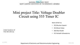
  • 1. Department of Electronics and Telecommunication Engineering Department of Electronics and Telecommunication Engineering Mini project Title: Voltage Doubler Circuit using 555 Timer IC 11-10-2023 1/total slides Name & Roll no: • 352 Bhushan Sawant • 353 Bharat Yadav • 360 Afzal Shaikh • 371 Rishabh Vishwakarma Under Guidance of Prof. M.K.Ahirrao
  • 2. Department of Electronics and Telecommunication Engineering Outline of the Presentation Introduction Background Circuit Design Testing and Results Results and Conclusion 2 Introduction Background Circuit Design Testing and Results Conclusions
  • 3. Department of Electronics and Telecommunication Engineering Introduction • Motivation • Background • Block diagram 3 Background Circuit Design Testing and Results Conclusions Introduction
  • 4. Department of Electronics and Telecommunication Engineering Motivation • The motivation for creating a voltage doubler circuit using a 555 timer IC lies in the educational value, practical applications, and the opportunity for hands-on learning and experimentation in the field of electronics. This project can serve as an exciting and informative way to enhance your electronics knowledge and skills. 4 Background Circuit Design Testing and Results Conclusions Introduction
  • 5. Department of Electronics and Telecommunication Engineering Background • This project offers an opportunity to learn and gain practical experience in electronics. It involves understanding the functioning of the 555 timer IC, diodes, capacitors, and voltage doubling principles, which are fundamental in electronics 5 Background Circuit Design Testing and Results Conclusions Introduction
  • 6. Department of Electronics and Telecommunication Engineering Block Diagram 6 Background Circuit Design Testing and Results Conclusions Introduction 5 5 5 Timer IC Power supply (5v) Resistors Capacitors 1N4007 Diode Multimeter /Voltmeter
  • 7. Department of Electronics and Telecommunication Engineering Background • Concepts • History 7 Circuit Design Testing and Results Conclusions Introduction Background
  • 8. Department of Electronics and Telecommunication Engineering Concepts The capacitor allows AC current to pass through it, but the diode only allows current to flow in one direction. This creates a peak output voltage of 2*V pk across the diode. This extremely simple circuit illustrates the concept, but it does not regulate the output DC voltage very well 8 Circuit Design Testing and Results Conclusions Introduction Background
  • 9. Department of Electronics and Telecommunication Engineering History Greinacher circuit The Greinacher voltage doubler is a significant improvement over the Villard circuit for a small cost in additional components. The ripple is much reduced, nominally zero under open-circuit load conditions, but when current is being drawn depends on the resistance of the load and the value of the capacitors used. The circuit works by following a Villard cell stage with what is in essence a peak detector or envelope detector stage. The peak detector cell has the effect of removing most of the ripple while preserving the peak voltage at the output. The Greinacher circuit is also commonly known as the half-wave voltage doubler. 9 Circuit Design Testing and Results Conclusions Introduction Background
  • 10. Department of Electronics and Telecommunication Engineering Circuit Design & Working • Circuit Interfacing Diagram. • Working • Main components and their specifications and principle of operation. • Applications. 10 Testing & Results Conclusions Introduction Background Circuit Design
  • 11. Department of Electronics and Telecommunication Engineering Circuit Interfacing Diagram. 11 Testing & Results Conclusions Introduction Background Circuit Design
  • 12. Department of Electronics and Telecommunication Engineering Working 12 Testing & Results Conclusions Introduction Background Circuit Design • A voltage doubler circuit using a 555 timer IC is an electronic circuit that takes an input voltage and produces an output voltage that is approximately double the input voltage. The circuit operates by generating an oscillating square wave signal using the 555 timer in its astable mode and then using diodes and capacitors to double the voltage
  • 13. Department of Electronics and Telecommunication Engineering Components • 555 Timer IC • 1N4007 Diode -2 • Resistors 10K • Resistor 33K • Capacitor 22uF – 2 • Capacitor 0.01uF – 2 • 3V-12V Battery 13 Testing & Results Conclusions Introduction Background Circuit Design
  • 14. Department of Electronics and Telecommunication Engineering Components specifications 555 Timer IC : • In astable mode, the 555 timer IC generates a continuous square wave output with a specific frequency and duty cycle. The frequency and duty cycle are determined by the resistors R1 and R2 and capacitor C1 connected to pins 2, 6, and 7 of the IC. • 1N4007 Diode : • 1N4007 rectifier diode has in total 2 pins, owns a cathode (-) and anode (+). In the schematic symbol, the tip of the triangle with the line on top of it is the cathode. The cathode is marked on the body of a diode by a band. It allows current flow through only one direction that means the anode to the cathode only and never from the cathode to the anode – it likes a one current can flow from way value. 14 Testing & Results Conclusions Introduction Background Circuit Design
  • 15. Department of Electronics and Telecommunication Engineering • Resistors: • A resistor is the most basic electronic component invariably found almost every electronic circuit. It is a passive element. The most important function of resistor is to resist the flow of current. The property of a resistor is known as resistance. • Capacitor: • It provides the value of a capacitor C as farads moreover printed or color coded over the body of the capacitor. Its units are Farads. Practical capacitors are available from 1pf to 1000 mF. 15 Testing & Results Conclusions Introduction Background Circuit Design
  • 16. Department of Electronics and Telecommunication Engineering Applications • Low-power Devices • LED Drivers • Photoflash Units • LCD Displays • RF Transmitters • Lab Experiments and Prototyping 16 Testing & Results Conclusions Introduction Background Circuit Design
  • 17. Department of Electronics and Telecommunication Engineering Testing & Results This circuit's operation is the switching action of the diodes and the energy transfer between the capacitors during each cycle of the 555 timer's square wave signal. By continuously repeating this process, the circuit effectively doubles the input voltage, making it useful in various applications where a higher voltage is required from a lower voltage power source. 17 Introduction Background Circuit Design Conclusions Testing and Results
  • 18. Department of Electronics and Telecommunication Engineering Testing 18 Introduction Background Circuit Design Conclusions Testing and Results
  • 19. Department of Electronics and Telecommunication Engineering Result 19 Introduction Background Circuit Design Conclusions Testing and Results
  • 20. Department of Electronics and Telecommunication Engineering Conclusion • Summary • Future Works • Precautions 20 Introduction Background Circuit Design Testing and Results Conclusions
  • 21. Department of Electronics and Telecommunication Engineering Summary • The circuit is the one which doubles the voltage and consists of 2 capacitors and 2 diodes connected in the manner shown in the circuit diagram. The 555-timer has multiple modes in which we have decided today to use astable Multivibrator mode. This mode can be used to generate a square wave of approximately 2KHz using a combination of two resistors and a capacitor. From the circuit, we can see that when the pin 3 of the timer IC has a low output, then the diode D1 gets forward biased, which will charge capacitor C3 through it. • Because the capacitor is charged directly from the supply, the capacitor will also get charged to the voltage equal to the input voltage. When the pulse from the timer IC is high, the pin 3 of the IC will show a high output. This will make the diode D1 reversed biased, and this blocks the charging of the capacitor C3 which has now been charged to approximately the voltage equal to the supply voltage. • When the diode D1 is reversed biased, the diode D2 will be forward biased, and this will charge the capacitor C4 through it. C4 capacitor will also be charge with the energy stored in capacitor C3. Now the capacitor C4 has double the voltage of the input voltage because it is charged via two paths one from the capacitor C3 which was charged initially to the supply voltage and another path is directly through the supply. • In theory, the output of this circuit must produce a voltage at the output equal to double the voltage at the input, but in reality, the charging and discharging of a capacitor is not a lossless process, the energy stored in a capacitor is not fully transmitted to the other capacitor, and the charging of the capacitor is also not ideal. 21 Introduction Background Circuit Desing Testing and Results Conclusions
  • 22. Department of Electronics and Telecommunication Engineering Further Improvements • We can cascade the diode-capacitor arrangement at the output of 555 timer IC to generate much higher voltages. The resulting circuit is called as a voltage multiplier circuit. It outputs a certain times input voltage as output voltage. The factor by which the output voltage is more than the input voltage is determined by the number of stages of capacitor+diode charge pump blocks used 22 Introduction Background Circuit Working Testing and Results Conclusions
  • 23. Department of Electronics and Telecommunication Engineering Precautions • Due to the limitations of the timer IC, the input voltage of the circuit cannot be greater than 12V and less than 3V, choosing a voltage between 3 and 12V will ensure safe working and no damage will be done to the components. • As discussed above, the working of the circuit depends on the charging and discharging of capacitors, and hence, the circuit will not give output of required value right away as soon as the circuit is plugged in with a supply voltage, but it will take a while before it settles at double the input voltage. 23 Introduction Background Circuit Working Testing and Results Conclusions
  • 24. Department of Electronics and Telecommunication Engineering Thank You 24
  • 25. Department of Electronics and Telecommunication Engineering References • https://how2electronics.com/voltage-doubler-circuit-using-555- timer-ic/ 25