This document provides the electrical characteristics, maximum ratings, and package dimensions for the S TM4433A P-channel enhancement mode field effect transistor. Key specifications include:
- Drain-source voltage rating of -30V
- Continuous drain current of 2.5A and pulsed drain current of 6A
- On-resistance of 35mOhm at VGS=-10V and 55mOhm at VGS=-4.5V
- Surface mount SO-8 package with a junction-to-ambient thermal resistance of 50°C/W
Original Mosfet Driver AO4407A 4407A 4407 SOP-8 New Alpha&OmegaAUTHELECTRONIC
Original Mosfet Driver AO4407A 4407A 4407 SOP-8 New Alpha&Omega
https://authelectronic.com/original-mosfet-driver-ao4407a-4407a-4407-sop-8-new-alpha-omega
Datasheet Layout for Semiconductor CompaniesAyça Little
Engineers have their own visual language which they use to communicate information about their products. Visual aids such as charts, graphs, tables, diagrams, mathematical symbols, detailed product blueprints and engineering drawings are all used to describe the product or application on offer.
It may seem like a cliché, but in many companies around the world, marketing and engineering departments often don't come into contact with each other and when they do they don’t always see eye to eye.
It is important for companies to come up with a system and workflow processes that allow for efficient communication and information sharing between these two departments so that products can be properly described and marketed. Effective use of technical documentation can lead to greater customer engagement and therefore more successful product sales and customer experiences.
Original PolarHV HiPerFET Power MOSFET IXFH44N50P 44N50 TO-3P 44A 500V New IX...AUTHELECTRONIC
Original PolarHV HiPerFET Power MOSFET IXFH44N50P 44N50 TO-3P 44A 500V New IXYS Corporation
https://authelectronic.com/original-polarhv-hiperfet-power-mosfet-ixfh44n50p-44n50-to-3p-44a-500v-new-ixys-corporation
Original Dual P-Channel Mosfet RF7316TRPBF IRF7316 F7316 7316 SOP-8 New IRAUTHELECTRONIC
Original Dual P-Channel Mosfet RF7316TRPBF IRF7316 F7316 7316 SOP-8 New IR
https://authelectronic.com/original-dual-p-channel-mosfet-rf7316trpbf-irf7316-f7316-7316-sop-8-new-ir
Original Power MOSFET IRFP140PBF IRFP140 IRFP140N 100V 33A TO-247 New Intern...AUTHELECTRONIC
Original Power MOSFET IRFP140PBF IRFP140 IRFP140N 100V 33A TO-247 New International Rectifier
https://authelectronic.com/original-power-mosfet-irfp140pbf-irfp140-irfp140n-100v-33a-to-247-new-international-rectifier
Original N-CHANNEL Mossfet IRFB4227PBF IRFB4227 4227 130A 200V TO-220 New IRAUTHELECTRONIC
Original N-CHANNEL Mossfet IRFB4227PBF IRFB4227 4227 130A 200V TO-220 New IR
https://authelectronic.com/original-n-channel-mossfet-irfb4227pbf-irfb4227-4227-130a-200v-to-220-new-ir
Original N-CHANNEL Mosfet CEP50N06 50N06 50A 60V TO-220 New AUTHELECTRONIC
Original N-CHANNEL Mosfet CEP50N06 50N06 50A 60V TO-220 New
https://authelectronic.com/original-n-channel-mosfet-cep50n06-50n06-50a-60v-to-220-new-thinki-semiconductor
Original N-Channel Mosfet IRF2907ZPBF 2907 75V 170A TO-220 New IRAUTHELECTRONIC
Original N-Channel Mosfet IRF2907ZPBF 2907 75V 170A TO-220 New IR
https://authelectronic.com/original-n-channel-mosfet-irf2907zpbf-2907-75v-170a-to-220-new-ir
Original N Channel Mosfet FQPF12N60 12N60 12A 600V New FairchildAUTHELECTRONIC
Original N Channel Mosfet FQPF12N60 12N60 12A 600V New Fairchild
https://authelectronic.com/original-n-channel-mosfet-fqpf12n60-12n60-12a-600v-new-fairchild
Original Mosfet IRFB18N50KPBF IRFB18N50K FB18N50K 18N50K 500V 17A TO-220 New ...AUTHELECTRONIC
Original Mosfet IRFB18N50KPBF IRFB18N50K FB18N50K 18N50K 500V 17A TO-220 New International Rectifier
https://authelectronic.com/original-mosfet-irfb18n50kpbf-irfb18n50k-fb18n50k-18n50k-500v-17a-to-220-new-international-rectifier
Original P-CHANNEL MOSFET IRF5210PBF IRF5210 5210 100V 38A TO-220 New IRAUTHELECTRONIC
Original P-CHANNEL MOSFET IRF5210PBF IRF5210 5210 100V 38A TO-220 New IR
https://authelectronic.com/original-p-channel-mosfet-irf5210pbf-irf5210-5210-100v-38a-to-220-new-ir
Original N-Channel Mosfet IC 20N15GH 20N15 TO-252 New Advanced Power Electron...
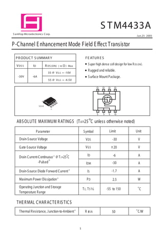
Stm4433a
1. -30
ABSOLUTE MAXIMUM RATINGS (TA=25 C unless otherwise noted)
Parameter Symbol Limit Unit
Drain-Source Voltage VDS V
Gate-Source Voltage VGS V
Drain Current-Continuous @ TJ=25 C
-Pulsed
ID
-30
-1.7
2.5
A
A
A
W
IDM
Drain-Source Diode Forward Current IS
Maximum Power Dissipation PD
Operating Junction and Storage
Temperature Range
TJ, TSTG -55 to 150 C
THERMAL CHARACTERISTICS
Thermal Resistance, Junction-to-Ambient R JA 50 /W
C
S TM4433A
a
a
a
a
b
1 2 3 4
8 7 6 5
S S S G
D D D D
5
1
S amHop Microelectronics Corp.
Surface Mount Package.
PR ODUCT S UMMAR Y
VDS S ID R DS (ON) ( m W ) Max
-6A
35 @ VGS = -10V
55 @ VGS = -4.5V
FE ATUR E S
Super high dense cell design for low RDS(ON).
Rugged and reliable.
S O-8
1
-30V
20
-6
Jan.25 2005
P-Channel Enhancement Mode Field Effect Transistor
2. S TM4433A
ELECTRICAL CHARACTERISTICS (TA 25 C unless otherwise noted)
=
Parameter Symbol Condition Min Typ Max Unit
OFF CHARACTERISTICS
Drain-Source Breakdown Voltage BVDSS =
VGS 0V, ID -250uA
= -30 V
Zero Gate Voltage Drain Current IDSS VDS -24V, VGS 0V
= = -1 uA
Gate-Body Leakage IGSS VGS 20V, VDS 0V
= = 100 nA
ON CHARACTERISTICS b
Gate Threshold Voltage VGS(th) VDS VGS, ID = -250uA
= -1 -3.0 V
Drain-Source On-State Resistance RDS(ON)
VGS -10V, ID -5.8A 35
VGS -4.5V, ID -2.0A 55
On-State Drain Current ID(ON) VDS = -5V, VGS = -10V -20 A
S
Forward Transconductance FS
g VDS -15V, ID - 5.8A
DYNAMIC CHARACTERISTICS
c
InputCapacitance CISS
CRSS
COSS
OutputCapacitance
Reverse Transfer Capacitance
VDS =-15V, VGS = 0V
f =1.0MHZ
PF
PF
PF
SWITCHING CHARACTERISTICS
c
Turn-On Delay Time
Rise Time
Turn-Off Delay Time
tD(ON)
tr
tD(OFF)
tf
VD = -15V,
ID = -1A,
VGEN = - 10V,
RGEN = 6 -ohm
ns
ns
ns
ns
Total Gate Charge
Gate-Source Charge
Gate-Drain Charge
Qg
Qgs
Qgd
VDS =-15V, ID = -5.8A,
VGS =-10V
nC
nC
nC
C
Fall Time
=
=
=
=
= =
5
2
m-ohm
m-ohm
nC
VDS=-15V, ID=-5.8A,VGS=-10V
VDS=-15V, ID=-5.8A,VGS=-4.5V
8.5
920
270
170
8.6
35.3
36.9
36.3
17.5
9.4
2.9
4.8
-1.9
21
40
3. S TM4433A
Parameter Symbol Condition Min Typ Max Unit
ELECTRICAL CHARACTERISTICS (TA=25 C unless otherwise noted)
C
DRAIN-SOURCE DIODE CHARACTERISTICS
Diode Forward Voltage VSD VGS = 0V, Is =-1.7A -0.77 -1.2 V
b
Notes
a.Surface Mounted on FR4 Board, t<=10sec.
c.Guaranteed by design, notsubjectto production testing.
b.Pulse Test:Pulse Width<=300us, Duty Cycle<= 2%.
Figure 1. Output Characteristics Figure 2. Transfer Characteristics
Figure 3. Capacitance
-VDS , Drain-to S ource Voltage (V)
-VGS , Gate-to-S ource Voltage (V)
-VDS , Drain-to-S ource Voltage (V)
C
,
C
apacitance
(pF
)
-I
D
,
Drain
C
urrent
(A)
-I
D
,
Drain
C
urrent
(A)
20
16
12
8
4
0
0 0.5 1.0 1.5 2.0 2.5 3.0
3
Figure 4. On-R esistance Variation with
Temperature
On-R
es
is
tance
R
DS
(ON)
,
Tj, J unction Temperature ( C )
(Normalized)
0 5 10 15 20 25 30
Ciss
Coss
1500
1250
1000
750
500
250
0
Crss
25 C
25
20
15
10
5
0
0
-55 C
125 C
1.8
1.6
1.2
0.8
1.4
1.0
0.6
0 25 75 125
50
-25
-55 100
VG S =-10V
ID=-5.8A
0.8 4.8
4.0
3.2
2.4
1.6
-VGS =2V
-VGS =3V
-VGS =3.5V
-VGS =4V
-VGS =4.5V
-VGS =10V
4. S TM4433A
Figure 5. G ate Threshold Variation
with Temperature
Figure 6. Breakdown Voltage Variation
with Temperature
V
th,
Normalized
G
ate-S
ource
T
hres
hold
V
oltage
g
F
S
,
T
rans
conductance
(S
)
-V
G
S
,
G
ate
to
S
ource
V
oltage
(V
)
B
V
DS
S
,
Normalized
Drain-S
ource
B
reakdown
V
oltage
-Is
,
S
ource-drain
current
(A)
Figure 7. Transconductance Variation
with Drain C urrent
-IDS , Drain-S ource C urrent (A)
Figure 9. G ate C harge
Qg, Total Gate Charge (nC)
Figure 10. Maximum S afe
Operating Area
-VDS , Drain-S ource Voltage (V)
Figure 8. Body Diode Forward Voltage
Variation with S ource C urrent
-VS D, Body Diode Forward Voltage (V)
Tj, Junction Temperature ( C ) Tj, J unction Temperature ( C )
-I
D
,
Drain
C
urrent
(A)
4
5
1.3
1.2
1.1
1.0
0.6
0.8
0.4
-50 -25 0 25 50 75 100 125 150
VDS =VGS
ID=-250uA
-50 -25 0 25 50 75 100 125 150
1.3
1.2
1.1
1.0
0.9
0.8
0.7
ID=-250uA
15
12
0
3
6
9
0 5 10 15 20
VDS =-15V
20.0
10.0
1.0
0.4 0.6 0.7 0.9 1.1 1.3
VGS =0V
8
10
6
4
2
0
0 3 6 9 12 15 18 21 24
VDS=-15V
ID=-5.8A
50
10
1
0.1
0.03
0.1 1 10 30 50
VGS=-10V
Single Pulse
TA=25 C
RDS(ON) Limit
10ms
100ms
1s
DC
5. Figure 11. S witching Test Circuit Figure 12. S witching Waveforms
t
V
V
t
t
d(on)
OUT
IN
on
r
10%
td(off)
90%
10% 10%
50% 50%
90%
toff
tf
90%
PULSE WIDTH
T
ransient
T
hermal
Impedance
2
1
0.1
0.01
S quare Wave Pulse Duration (sec)
Figure 13. Normalized Thermal Transient Impedance Curve
r(t),Normalized
E
ffective
5
5
S TM4433A
INVERTED
Duty Cycle=0.5
0.2
0.1
0.05
0.02
S ingle Pulse
10
-4
10
-3
10
-2
10
-1
1 10 100
PDM
t1
t2
1. R thJA (t)=r (t) * R thJA
2. R thJA=S ee Datasheet
3. TJM-TA = PDM* R thJA (t)
4. Duty Cycle, D=t1/t2
-VDD
R
D
V
V
R
S
V
G
GS
IN
GE N
OUT
L
6. PACKAGE OUTLINE DIME NS IONS
S O-8
6
S YMBOLS
MIN MIN
0.053
0.004
0.189
0.150
0.228
0.016
0°
1.35
0.10
4.80
3.81
5.79
0.41
0°
MAX MAX
0.069
0.010
0.196
0.157
0.244
0.050
8°
1.75
0.25
4.98
3.99
6.20
1.27
8°
MILLIME TE R S INCHE S
A
A1
D
E
H
L
1
e B
H
E
L
A1
A
C
D
0.05 TYP. 0.016 TYP.
0.008
TYP.
0.015X45°
S TM4433A
7. SO-8 Tape and Reel Data
SO-8 Carrier Tape
SO-8 Reel
unit:㎜
PACKAGE
SOP 8N
150㏕
A0 B0 K0 D0 D1 E E1 E2 P0 P1 P2 T
6.40 5.20 2.10
ψ1.5
(MIN)
ψ1.5
+ 0.1
- 0.0
12.0
±0.3
1.75
5.5
±0.05
8.0 4.0 2.0
±0.05
0.3
±0.05
UNIT:㎜
TAPE SIZE
12 ㎜
REEL SIZE
ψ330
M N W W1 H K S G R V
330
± 1
62
±1.5
12.4
+ 0.2
16.8
- 0.4
ψ12.75
+ 0.15
2.0
±0.15
S TM4433A
7