Downloaded 84 times


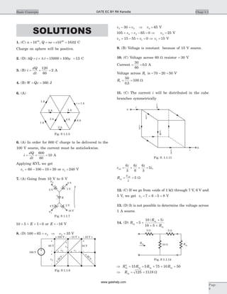


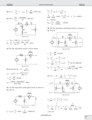
![This in similar to matrix in (A). Only place of rows has
been changed.
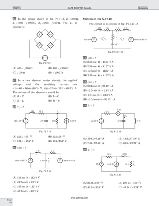
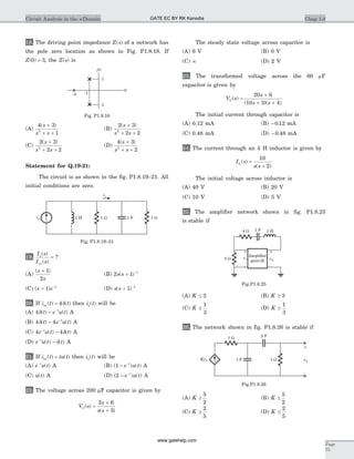
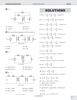
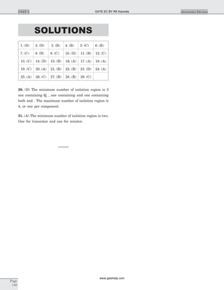
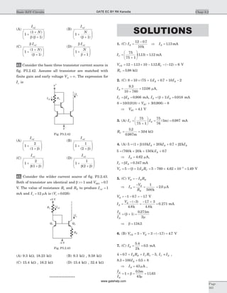
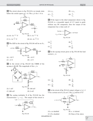
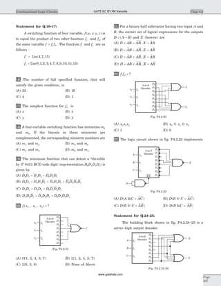
27. (A) Number of branch =8
Number of link =4
Number of twigs =8 4 4- =
Number of twigs =number of independent node
equation.
28. (D) The number of independent node equation are
n - 1.
29. (A) Number of branch b = 8
Number of link l = 4
Number of twigs t b l= - = 4
rank of matrix = - = =n t1 4
30. (B) We know the branch current and loop current
are related as
[ ] [ ][ ]i B Ib
T
L=
So fundamental loop matrix is
Bf =
-
-
- -
- -
é
ë
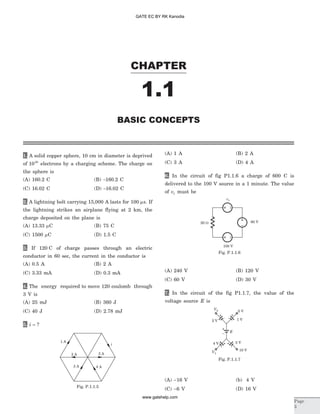
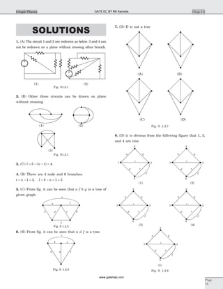
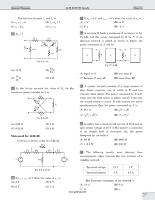
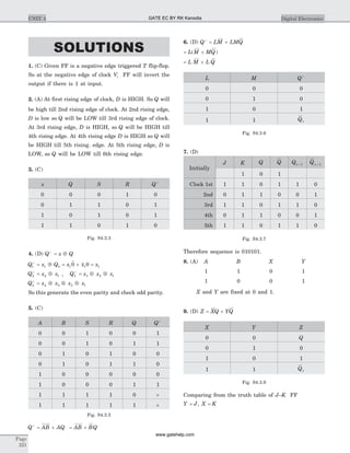
ê
ê
ê
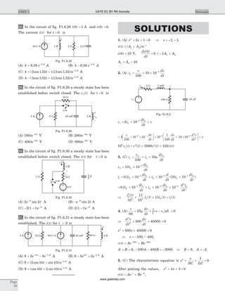
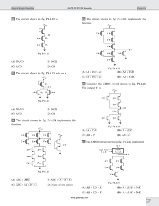
ê
ù
û
ú
0 1 0 1 0 1 1 0
0 1 1 0 0 1 0 0
1 1 0 0 1 0 0 0
0 0 0 0 1 1 0 1
ú
ú
ú
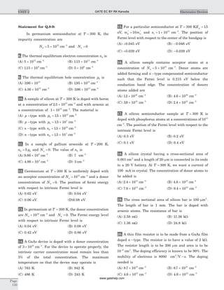
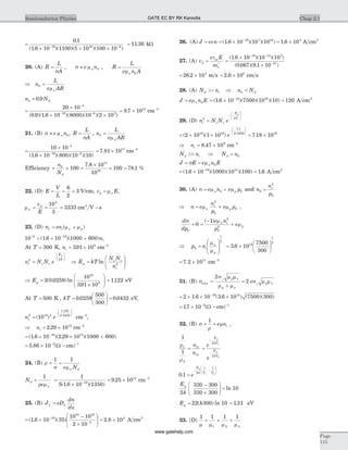
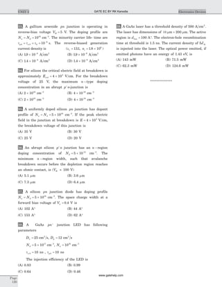
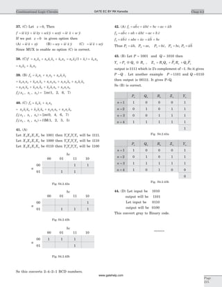
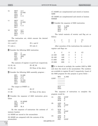
f-loop 1 include branch (2, 4, 6, 7) and direction of
branch–2 is opposite to other (B only).
31. (B) Independent loops =link
l b n= - -( )1
Þ = -5 7b , b = 12
32. (B) Independent loop =link
l b n= - - =( )1 4
33. (A) There are 8 branches and 4 1 5+ = node
Number of link = - + =8 5 1 4
So independent mesh equation =Number of link.
34. (D) We know that [ ] [ ]v A Vb r
T
n=
So reduced incidence matrix is
Ar =
-
- -
-
é
ë
ê
ê
ê
ê
ù
û
ú
ú
ú
1 0 0 0 1 0 0 1
0 1 0 0 1 1 0 0
0 0 1 0 0 1 1 1
0 0 0 1 0 0 1 0ú
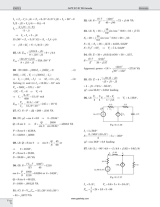
At node-1, three branch leaves so the only option is (D).
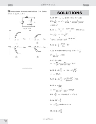
***********
Page
22
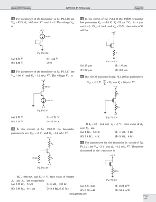
NetworksUNIT 1
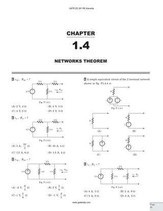
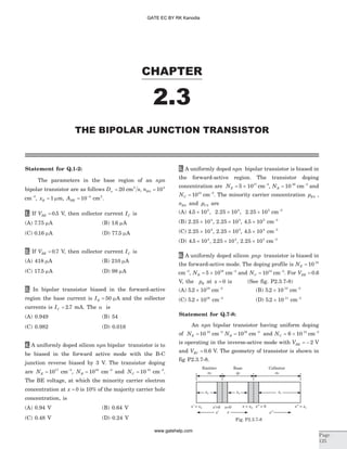
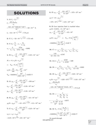
g
bh
a
c
i
e
d fl3
l4
l1
l2
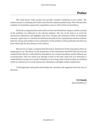
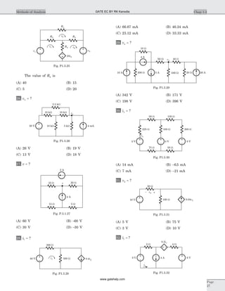
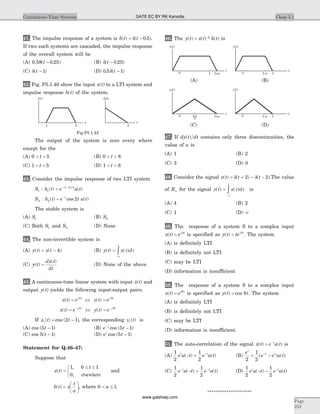
Fig. S 1.2.26
GATE EC BY RK Kanodia
www.gatehelp.com](https://image.slidesharecdn.com/a-150815031147-lva1-app6892/85/A-gate-by-rk-kanodia-21-320.jpg)
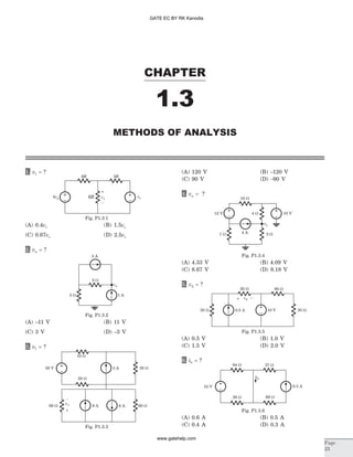

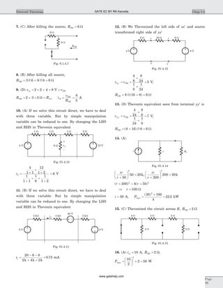

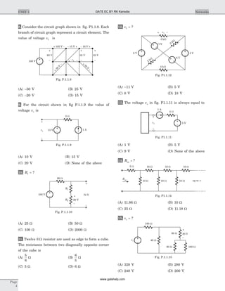
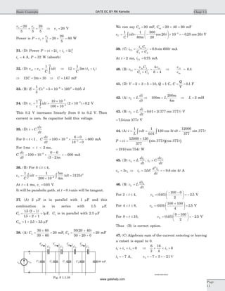
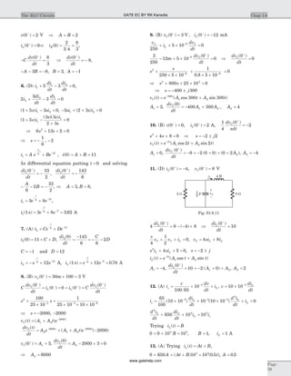
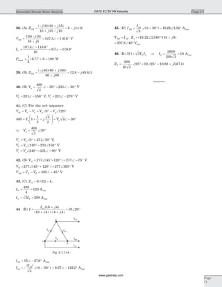
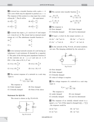
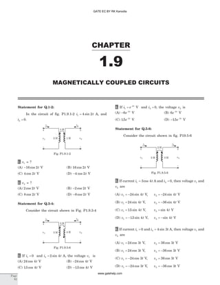
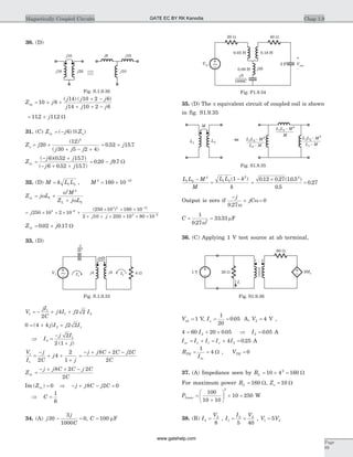
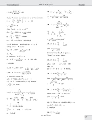
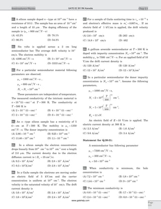
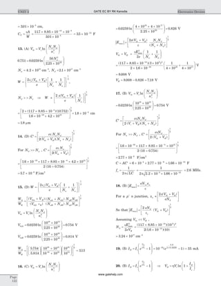
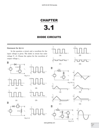
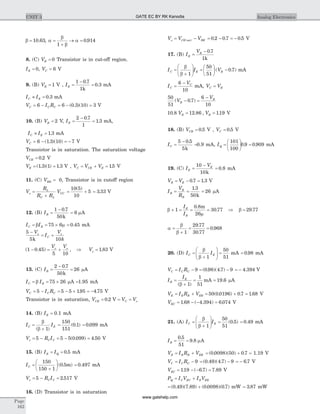
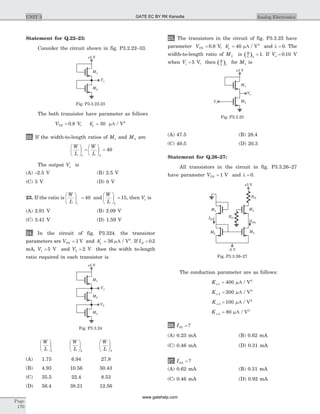
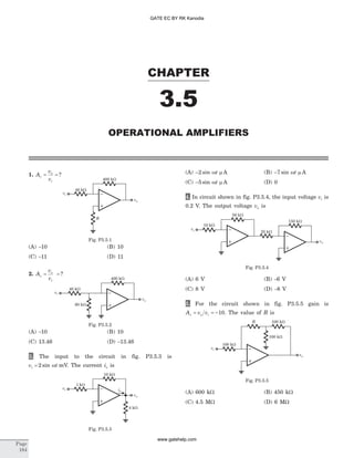
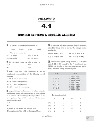
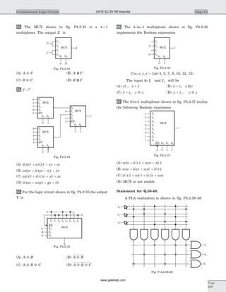
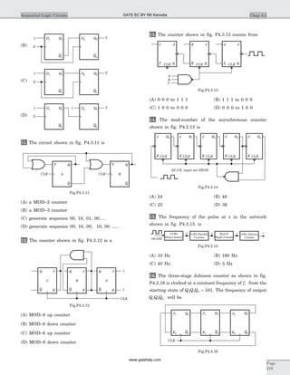
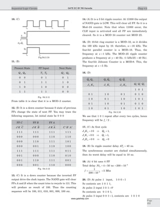
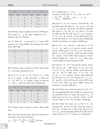
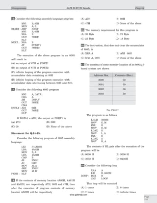
![Statement for Q.6–7:
Circuit is shown in fig. P.1.6. Initial conditions are
i i1 20 0 11( ) ( )= = A
6. i1 1( )s = ?
(A) 0.78 A (B) 1.46 A
(C) 2.56 A (D) 3.62 A
7. i2 1( )s = ?
(A) 0.78 A (B) 1.46 A
(C) 2.56 A (D) 3.62 A
8. v tC( ) = ? for t > 0
(A) 4 1000 2000
e et t- -
- V (B) ( )3 6000 2000
+ -
t e t
V
(C) 2 1000 2000
e et t- -
+ V (D) ( )3 6000 2000
- -
t e t
V
9. The circuit shown in fig. P1.6.9 is in steady state
with switch open. At t = 0 the switch is closed. The
output voltage v tC( ) for t > 0 is
(A) - +- -
9 12400 300
e et t
(B) e t tt-
+400
3 300 4 300[ cos sin ]
(C) e t tt-
+300
3 400 4 300[ cos sin ]
(D) e t tt-
+300
3 400 2 25 300[ cos . sin ]
10. The switch of the circuit shown in fig. P1.6.10 is
opened at t = 0 after long time. The v t( ) , for t > 0 is
(A) 4 22
e tt-
sin V (B) - -
4 22
e tt
sin V
(C) 4 22
e tt-
cos V (D) - -
4 22
e tt
cos V
11. In the circuit of fig. P1.6.23 the switch is opened at
t = 0 after long time. The current i tL ( ) for t > 0 is
(A) e t tt-
+2
2 4( cos sin ) A (B) e t tt-
-2
3 4( sin cos ) A
(C) e t tt-
- +2
4 2( sin cos ) A (D)e t tt-
-2
2 4( sin cos ) A
Statement for Q.12–14:
In the circuit shown in fig. P1.6.12–14 all initial
condition are zero.
12. If i ts( ) = 1 A, then the inductor current i tL ( ) is
(A) 1 A (B) t A
(C) t + 1 A (D) 0 A
13. If i t ts( ) .= 0 5 A, then i tL ( ) is
(A) 0 5 3 25 10 3
. .t + ´ -
A (B) 2 3250t - A
(C) 0 5 0 25 10 3
. .t - ´ -
A (D) 2 3250t + A
14. If i t es
t
( ) = -
2 250
A then i tL ( ) is
(A)
4000
3
250
te t-
A (B)
4000
3
250
e t-
A
(C)
200
7
250
e t-
A (D)
200
7
250
te t-
A
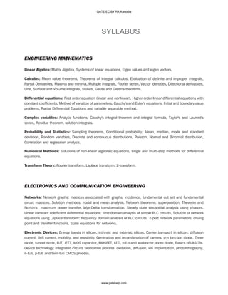
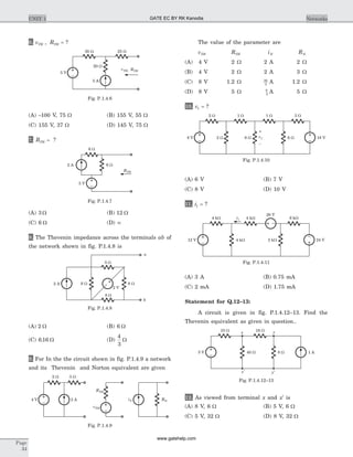
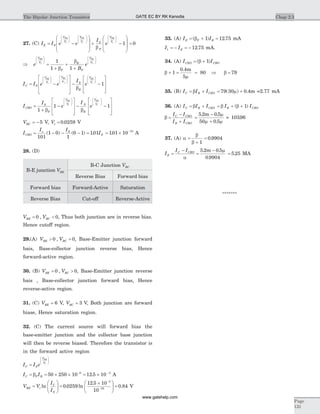
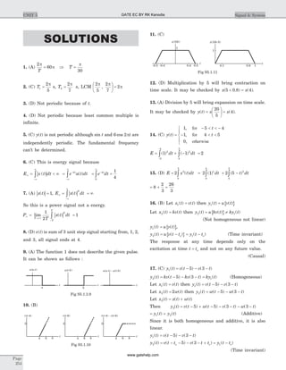
Chap 1.6The RLC Circuits
Page
55
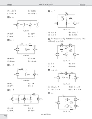
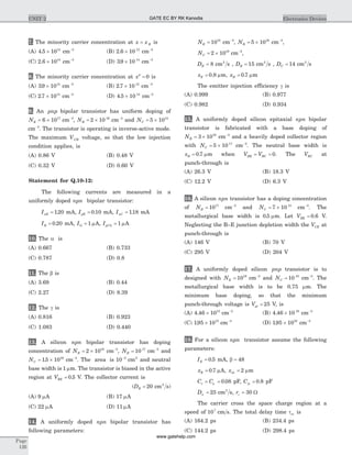
3 H1 W
2 H
2 W
i1 i2
Fig. P1.6.6–7
30 (- ) mAu t 10 Fm
25 mH
100 W vC
–
+
Fig. P1.6.8
0.8 H
500 W
9 V
250 W 5 Fm vC
–
+
t=0
Fig. P1.6.9
3 W
1 W H6 V
t=0
F2
1
4
1
vC
–
+
Fig. P1.6.10
2 W
t=0
4 H
7 A4 W
8 W
iL
F4
1
Fig. P1.6.11
W
100
65
i u ts ( ) A 1 mF
iL
vL
–
+
10 mH
Fig. P1.5.12-14
GATE EC BY RK Kanodia
www.gatehelp.com](https://image.slidesharecdn.com/a-150815031147-lva1-app6892/85/A-gate-by-rk-kanodia-38-320.jpg)
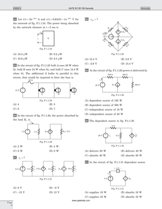
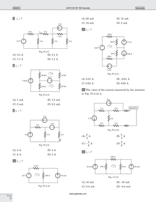
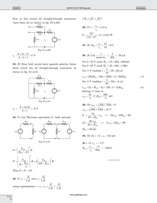
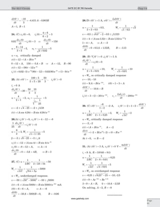
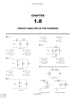
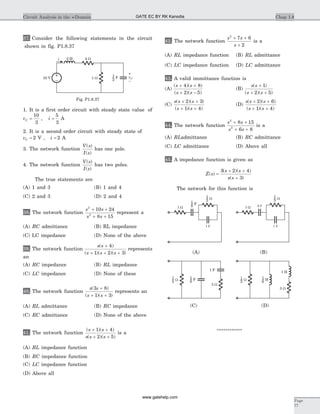
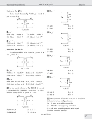
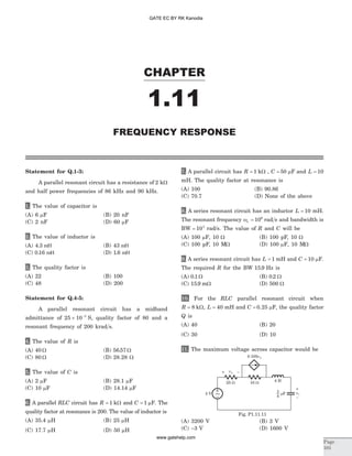
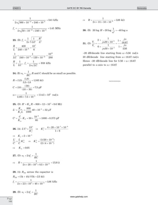
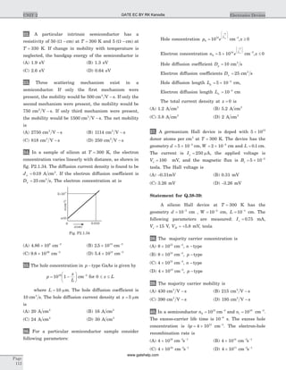
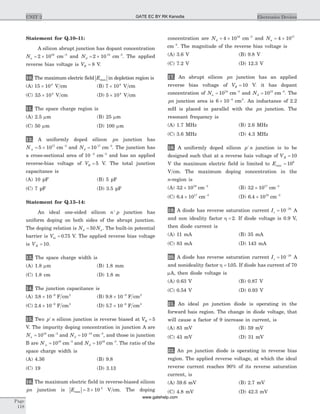
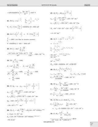
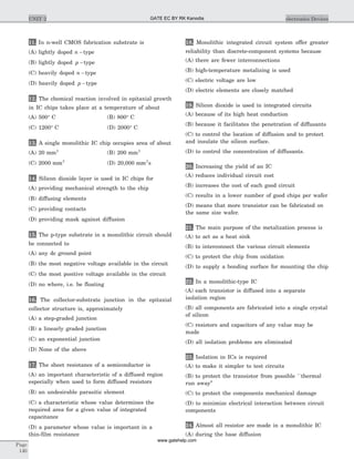
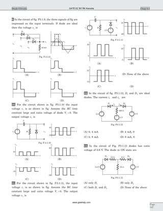
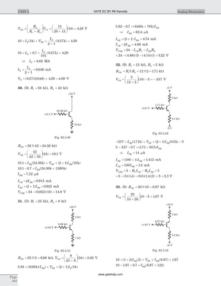
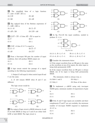
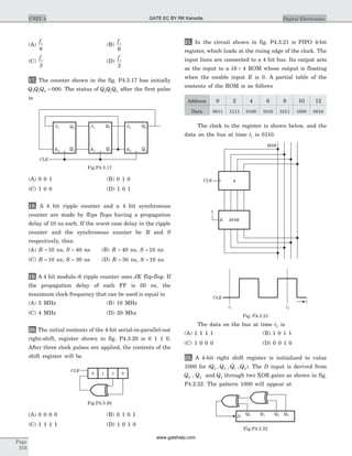
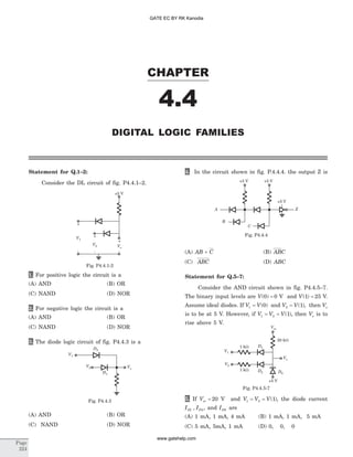
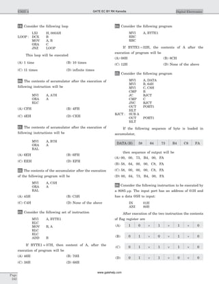
![15. The forced response for the capacitor voltage v tf ( ) is
(A) 0 2 117 10 3
. .t + ´ -
V (B) 0 2 117 10 3
. .t - ´ -
V
(C) 117 10 0 23
. .´ --
t V (D) 117 10 0 23
. .´ +-
t V
16. For a RLC series circuit R L= =20 0 6W , . H, the
value of C will be
[CD =critically damped, OD =over damped,
UD =under damped].
CD OD UD
(A) C = 6 mF C >6 mF C <6 mF
(B) C = 6 mF C < 6 mF C > 6 mF
(C) C >6 mF C = 6 mF C < 6 mF
(D) C <6 mF C =6 mF C > 6 mF
17. The circuit shown in fig. P1.6.17 is critically
damped. The value of R is
(A) 40 W (B) 60 W
(C) 120 W (D) 180 W
18. The step response of an RLC series circuit is given
by
d i t
dt
di t
dt
i t
2
2
5 10
( ) ( )
( )+ + = , i( )0 2+
= ,
di
dt
( )0
4
+
= .
The i t( ) is
(A) 1 4+ -
e tt
cos A (B) 4 2 4- -
e tt
cos A
(C) 2 4+ -
e tt
sin A (D) 10 4+ -
e tt
sin A
19. In the circuit shown in fig. P 1.5.19 v t( ) for t > 0 is
(A) 50 46 5 3 62 3 4
- + -
( . sin cos )t t e t
V
(B) 50 46 5 3 62 3 4
+ + -
( . sin cos )t t e t
V
(C) 50 62 4 46 5 4 3
+ + -
( cos . sin )t t e t
V
(D) 50 62 4 46 5 4 3
- + -
( cos . sin )t t e t
V
20. In the circuit of fig. P1.6.20 the switch is closed at
t = 0 after long time. The current i t( ) for t > 0 is
(A) -10 8sin t A (B) 10 8sin t A
(C) -10 8cos t A (D) 10 8cos t A
21. In the circuit of fig. P1.6.21 switch is moved from 8
V to 12 V at t = 0. The voltage v t( ) for t > 0 is
(A) 12 4 2 2 2- + -
( cos sin )t t e t
V
(B) 12 4 2 8 2- + -
( cos sin )t t e t
V
(C) 12 4 2 8 2+ + -
( cos sin )t t e t
V
(D) 12 4 2 2 2+ + -
( cos sin )t t e t
V
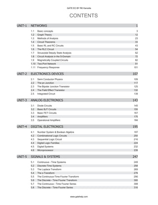
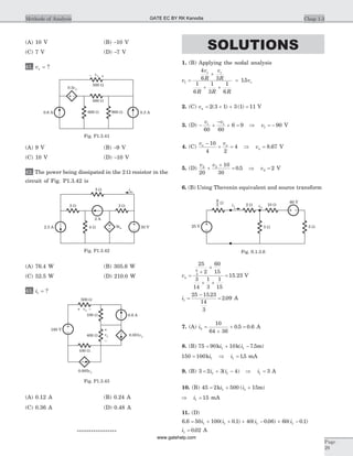
Page
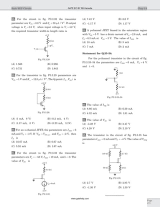
56
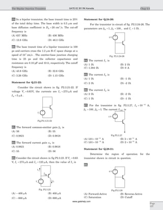
UNIT 1 Networks
120 WR
10 mF
4 H
Fig. P1.6.17
2 (- ) Au t
1 H 0.04 F
4 W 2 W
50 ( ) Vu t
vC –+
Fig. P1.6.19
5 W
iL
20 V
t=0
H
1
4
F
1
16
vC –+
Fig. P1.6.20
2 W
12 V
1 H
8 V F
1
6
vC
–
+
t=0
Fig. P1.6.21
vx– +
iL
20 mH50 Wavx
100 W
Fig. P1.6.15
GATE EC BY RK Kanodia
www.gatehelp.com](https://image.slidesharecdn.com/a-150815031147-lva1-app6892/85/A-gate-by-rk-kanodia-39-320.jpg)
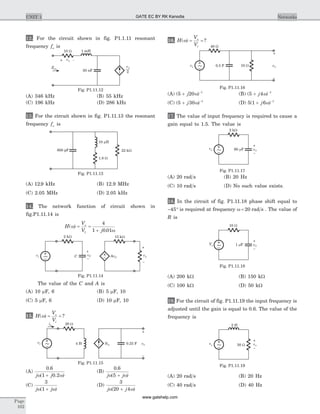
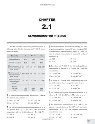
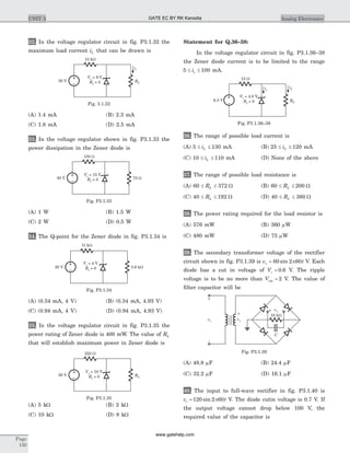
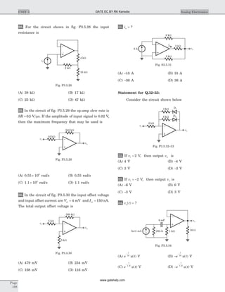
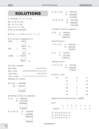
![15. (C) V
j
j j
o =
Ð °
+
- Ð °
+
+
-
+
= Ð - °
120 15
40 20
6 30
1
40 20
1
30
1
50
124 154
16. (C) 10 30sin ( )t + ° = - °10 60cos ( )t
V
j
j j
o =
Ð - °
+
Ð - °
+
-
+
10 60 20 45
3
1 1 1
3
= Ð - °+ Ð - °30 150 20 45
Vo = Ð - °315 112. V
17. (C) 5 0 4 1 1
4
1
4
1 2Ð ° = + + -
æ
è
ç
ö
ø
÷ - -
æ
è
ç
ö
ø
÷I j
j
I
j
Þ + - - = Ð( ) ( )8 15 4 20 01 2j I j I ...(i)
- Ð - ° = + + - - -10 30 1 4 1
4
1
4
2 1I j
j
I
j
( ) ( )
Þ - - + = Ð - °( ) ( )4 8 15 40 301 2j I j I ...(ii)
I j j1
2 2
8 15 4[( ) ( ) ]+ - -
= Ð + - Ð - ° -( )( ) ( )( )20 0 8 15 40 30 4j j
I j j1 176 248 41 43 414 64( ) . .- + = +
Þ = - = Ð -I j1 103 0 9 1 37 4107. . . .
18. (B) I
j j
j
2
8 15 103 0 9 20 0
4
=
+ - - Ð °
-
( )( . . )
= - +0 076 2 04. .j Þ = Ð °I2 2 04 92 13. .
19. (B) 10 30 4 0 5 21Ð ° = - + -I I j Ix x. ( )
( ) ( )- = -j I I I jx x2 31 , I
Ix
1
3
=
10 30
4
3
0 5 2Ð ° = - -
æ
è
ç
ö
ø
÷. j Ix Þ =
Ð °
Ð - °
Ix
10 30
2 17 67 38. .
20. (B) Let Vo be the voltage across current source
V V V V
j
o x o x-
+
-
=
4
20 10
3
V j j V jo x( ) ( )20 10 20 40 600+ - + =
V
V
j
V
V
jx
o
o
x
=
+
Þ = +
( )
( )
20
20 10 2
2
V
j j
j jx =
+ +
- +
æ
è
ç
ö
ø
÷ =
( )( )
( )
2 20 10
2
20 1 2 600
V
j
j
x =
- -
= Ð - °
600
5 20
29 22 166.
21. (A) I V
j V V
j
j V j V1 3
3 2
2 3
2 10
0 1 0 4=
æ
è
ç
ö
ø
÷ +
-
= +. .
= Ð ° Ð ° + Ð ° Ð - °( . )( . . ) ( . )( . . )0 1 90 0 757 66 7 0 4 90 0 606 69 8
Þ = Ð °I1 0 196 35 6. .
22. (A)
V V V
j
o o o
2
3
4
4 30+
-
= Ð - °
V j jo( . . ) .0 5 0 5 3 46 2+ = - Þ Vo = Ð - °5 65 75.
23. (D) I2 4 90= Ð ° , I3 2 0= Ð °
12 0 3 2 2 8 90 4 01Ð ° = - + + + Ð °- Ð °I j( )
Þ = +I j1 352 0 64. .
V j jo = + + = Ð °2 352 0 64 4 11 65 52 82( . . ) . . V
24. (D) I2 3 0= Ð ° A , I I4 3 6 0- = Ð ° A
I I I j I I j Io3 3 4 2 41 4 2 0( ) ( )( ) ( )( )+ - - + + + =
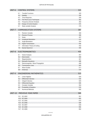
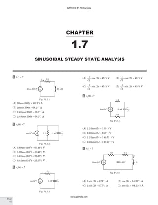
Chap 1.7Sinusoidal Steady State Analysis
Page
69
I2I1
- 3j j4
2 W12 0 VÐ
o
4 90 VÐ
o
2 W 2 W
Vo
–
+
2 0 AÐ o
~ ~
~
Fig. P1.7.23
I3
I4
I215 90 VÐ o
3 0 AÐ o
6 0 AÐ
o
2 W
j2
1 W 1 W
- 4j
Io
~
~~
Fig. S.1.7.24
5 0 VÐ
o
10 -30 VÐ
o
- 0.25j W
I1 I2
1 W 1 W
1 W
~ ~
j4j4
Fig. S.1.7.17
j1
- 1j W 20 -45 VÐ
o
Vo10 -60 VÐ
o
3 W
~ ~–
+
Fig. S.1.7.16
GATE EC BY RK Kanodia
www.gatehelp.com](https://image.slidesharecdn.com/a-150815031147-lva1-app6892/85/A-gate-by-rk-kanodia-49-320.jpg)
![(B)
2 3
1
3
3 2
1
12
0
1
2
+ + -
- +
é
ë
ê
ê
ê
ù
û
ú
ú
ú
é
ë
ê
ù
û
ú =
-
é
s
s
s
s
s
I s
I s
s( )
( )
ë
ê
ê
ê
ù
û
ú
ú
ú
(C)
2 3
1
3
3 2 3
1
12
1
2
+ + -
- + +
é
ë
ê
ê
ê
ù
û
ú
ú
ú
é
ë
ê
ù
û
ú =
-s
s
s
s s
s
I s
I s
( )
( )
s
0
é
ë
ê
ê
ê
ù
û
ú
ú
ú
(D)
2 3
1
3
3 2 3
1
12
1
2
+ + -
- + +
é
ë
ê
ê
ê
ù
û
ú
ú
ú
é
ë
ê
ù
û
ú =
s
s
s
s s
s
I s
I s
s( )
( ) 0
é
ë
ê
ê
ê
ù
û
ú
ú
ú
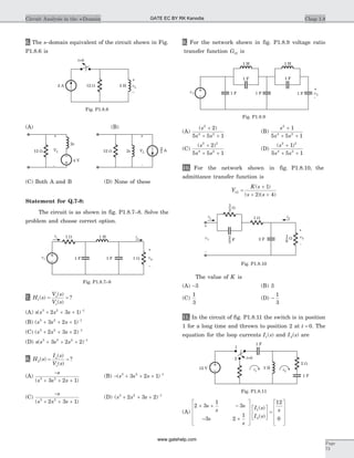
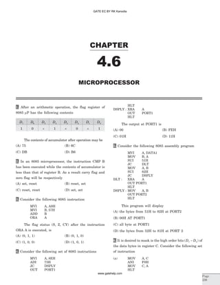
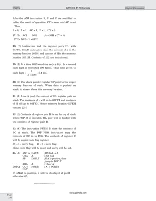
12. In the circuit of fig. P1.8.12 at terminal ab
Thevenin equivalent is
(A) V s
s
s s
Z s
s
s
TH TH( )
( )
( )
, ( )
( )
=
- +
+
=
- +8 2
3 1
2 1
3
(B) V s
s
s s
Z s
s
s
TH TH( )
( )
( )
, ( )
( )
=
+
+
=
+8 2
3 1
2 1
3
(C) V s
s
s s
Z s
s
s
TH TH( )
( )
( )
, ( )
( )
=
+
+
=
+4 3
3 1
2 1
6
(D) V s
s
s s
Z s
s
s
TH TH( )
( )
( )
, ( )
( )
=
- +
+
=
- +4 3
3 1
2 1
6
13. In the circuit of fig. P1.8.13 just before the closing of
switch at t = 0, the initial conditions are known to be
vC1 0 1( )-
= V, vC2 0 0( )-
= . The voltage v tC1( ) is
(A) u t( ) V (B) 0 5. ( )u t V
(C) 0 5. e t-
V (D) e t-
V
14. The initial condition at t = -
0 of a switched capacitor
circuit are shown in Fig. P1.8.14. Switch S1 and S2 are
closed at t = 0. The voltage v ta( ) for t > 0 is
(A) 9
t
V (B) 9e t-
V
(C) 9 V (D) 0 V
15. A unit step current of 1 A is applied to a network
whose driving point impedance is
Z s
V s
I s
s
s
( )
( )
( )
( )
( )
= =
+
+
3
2 2
The steady state and initial values of the voltage
developed across the source would be respectively
(A) 3
4
V, I V (B) 1
4
V, 3
4
V
(C) 3
4
V, 0 V (D) 1 V, 3
4
V
16. In the circuit of Fig. P1.8.16 i( )0 1= A, vC( )0 8=
V and v e u tt
1
2 10
2
4
= - ´
( ). The i t( ) is
(A) 1
15
10 2 10 4 10
10 3 22
4 4 4
[ ] ( )e e e u tt t t- - ´ - ´
- - A
(B) 1
15
10 2 10 4 10
10 3 22
4 4 4
[ ] ( )- + +- - ´ - ´
e e e u tt t t
A
(C) 1
3
10 2 10 4 10
10 3 22
4 4 4
[ ] ( )e e e u tt t t- - ´ - ´
+ + A
(D) 1
3
10 2 10 4 10
10 3 22
4 4 4
[ ] ( )- + -- - ´ - ´
e e e u tt t t
A
17. In the circuit shown in Fig. P1.8.18 v( )0 8-
= V and
i t tin ( ) ( )= 4d . The v tC( ) for t ³ 0 is
(A) 164e t-
V (B) 208e t-
V
(C) 208 1 3
( )- -
e t
V (D) 164 3
e t-
V
Page
74
UNIT 1 Networks
A 2 W Vo( )s
+
-
2Vo( )s
a
b
s
1
( +1)s
4
Fig. P1.8.12
1 F vC2
+
-
1 FvC1
+
-
t=0
Fig. P1.8.13
10 V
S1
5 V
Va
1 V
S2
5 V2 F
+
-
6 V
+-
3 F 4 F
+ -
Fig. P1.8.14
50 W 1m H
v1 2.5 Fm
i
vC
–
+
Fig. P1.8.16
iin 20 mF50 W vC
–
+
Fig. P1.8.17
GATE EC BY RK Kanodia
www.gatehelp.com](https://image.slidesharecdn.com/a-150815031147-lva1-app6892/85/A-gate-by-rk-kanodia-54-320.jpg)
![18. (B) Z s
K s
s j s j
K s
s s
( )
( )
( ( ))( ( ))
( )
=
+
- - + - -
=
+
+ +
3
1 1
3
2 22
Z
K
K( )0
3
2
3 2= = Þ =
19. (D)
I s
I s
s
s
s
s s
s
s
o
in
( )
( )
= +
+
+
+
=
+
1
1
1
1
1
20. (B) I sin ( ) = 4
I s
s
s s
o( ) =
+
= -
+
4
1
4
4
1
Þ i t t e u to
t
( ) ( ) ( )= - -
4 4d
21. (B) I s
s
in ( ) =
1
2
,
I s
s s s s
o( )
( )
=
+
= -
+
1
1
1 1
1
i t u t e u to
t
( ) ( ) ( )= - -
= - -
( ) ( )1 e u tt
22. (D) v sV s
s
s
C
s
C
s
( ) lim ( ) lim¥ = =
+
+
=
® ®0 0
2 6
3
2 V
23. (D) v sV sC
s
C( ) lim ( )0+
®¥
= =
+
+ +
=
s s
s s
( )
( )( )
20 6
10 3 4
2 V
i
Cdv
dt
C
C
= Þ I s C sV s vC C C( ) [ ( ) ( )]= - +
0
= ´
+
+ +
-
æ
è
çç
ö
ø
÷÷
-
60 10
20 6
10 3 4
26 s s
s s
( )
( )( )
=
- ´ +
+ +
-
480 10 10 3
10 43 12
6
2
( )s
s s
i sI sC
s
C( ) lim ( ) .0 480 10 0 486+
® ¥
-
= = - ´ = - mA
24. (A) v L
d i
dt
V s L sI s iL
L
L L L= Þ = - +
( ) [ ( ) ( )]0
i sI s
s
L
s
L( ) lim ( )0
10
2
0+
®¥
= =
+
=
V s
s
s s s
L ( )
( )
=
+
=
+
40
2
40
2
v sV s
s
s
L
s
L( ) lim ( )0
40
2
40+
®¥
= =
+
=
25. (A) V s KV s2 1( ) ( )=
Þ
V s V s KV s
s
s
1 1 1
2 4
1
0
( ) ( ) ( )
+
-
+ +
=
4
1
2 2 0+ + + - =s
s
K
Þ s K s2
6 2 1 0+ - + =( )
( )6 2 0- >K Þ K < 3
26. (B) Let v1 be the node voltage of middle node
V s
KV s sV s
s s
1
2 22
1 2
( )
( ) ( )
=
+
+ +
Þ + = +( ) ( ) ( ) ( )3 1 21 2s V s s K V s
Þ V s
sV s
s
2
12
2 1
( )
( )
=
+
Þ + =( ) ( ) ( )2 1 22 1s V s sV s
Þ + + = +( )( ) ( )3 1 2 1 2 2s s s s K
2 5 2 1 02
s K s+ - + =( ) ,
5 2 0- >K , K <
5
2
27. (A) H s
H s a
s
( )
( )
=
+
+ 4
R s
H s a
s s
Ha
s
H
a
s
( )
( )
( )
=
+
+
= +
-
æ
è
ç
ö
ø
÷
+4 4
1
4
4
r t
Ha
u t H
a
e t
( ) ( )= + -
æ
è
ç
ö
ø
÷
-
4
1
4
4
28. (A) V s
s
s
in ( ) =
+2
1
, I s
s
o( ) =
+
2
12
,
I s
V s s
o
in
( )
( )
=
2
29. (D) Z s
sL R
sC
sL R
sC
( )
( )
=
+
+ +
1
1
=
+
æ
è
ç
ö
ø
÷
+ +
1
12
C
s
R
L
s
R
L LC
Z s
K s
s j s j
( )
( )
=
+
+ +
æ
è
ç
ç
ö
ø
÷
÷ + -
æ
è
ç
ç
ö
ø
÷
÷
1
1
2
3
2
1
2
3
2
=
+
+ +
K s
s s
( )
( )
1
12
Since Z K( ) ,0 1 1= =thus
1
1 1
1
1
C
R
L LC
= = =, ,
Þ C L R= = =1 1 1, ,
30. (B) The characteristic equation is
s s s2 2
11 30 0( )+ + = Þ s s s2
6 5( ) ( )+ + =0
s = - -6 5, , Being real and unequal, it is overdamped.
Page
80
UNIT 1 Networks
sL
R
Cs
1Z s( )
Fig. S1.8.29
GATE EC BY RK Kanodia
www.gatehelp.com](https://image.slidesharecdn.com/a-150815031147-lva1-app6892/85/A-gate-by-rk-kanodia-58-320.jpg)
3 0 5 10 12 0 2 0j
= + = Ð °9 6 21 6 26 64 66 04. . . .j V
27. (A) [ ( ) ( ) ] ( )( . ) ( )j I j100 2 10 100 0 4 2 0 02p p+ + Ð =
Þ = - -I j2 0 4 0 0064. . ,
V I jo = = - -10 4 0 0642 .
= Ð - °4 179 1.
Þ = - °v to 4 100 179 1cos ( . )p V
28. (B) 30 30 6 8 4 12 4 10Ð ° = - + - + - +I j j j j j( )
Þ =
Ð °
+
= -I
j
j
30 30
10 6
2 57 0 043
( )
. .
V I j jo = - +( )12 4 10
= - +( . . )( )2 57 0 043 10 8j j
= +26 067 20 14. .j = Ð °32 9 37 7. . V
29. (A)
( )- + + - = -j j I jI j2 4 31 2
( )j I jI4 2 12 302 1+ - = - Ð ° V
I j1 1 45 0 56= - -. . ,
V I jx = - = +2 2 9 1121 . .
= Ð °311 2112. . V
Page
88
UNIT 1 Networks
3 H
2 H
5 H
-1 H
2 H
Fig. S.1.9.19
I1 I2
3 -90 AÐ o
+- Vx
-j
j4
j
12 30 VÐ
o
2 W 2 W
j4
~~
Fig. S1.9.29
GATE EC BY RK Kanodia
www.gatehelp.com](https://image.slidesharecdn.com/a-150815031147-lva1-app6892/85/A-gate-by-rk-kanodia-65-320.jpg)
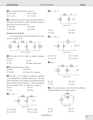
![Statement for Q.1-4:
The circuit is given in fig. P.1.10.1–4
1. [ ] ?z =
(A)
- -
-
é
ë
ê
ê
ê
ù
û
ú
ú
ú
1
2
3
2
17
6
1
2
(B)
1
2
3
2
17
6
1
2
é
ë
ê
ê
ê
ù
û
ú
ú
ú
(C)
- -
-
é
ë
ê
ê
ê
ù
û
ú
ú
ú
17
6
1
2
1
6
3
2
(D)
17
6
1
2
1
6
3
2
é
ë
ê
ê
ê
ù
û
ú
ú
ú
2. [ ] ?y =
(A)
3
8
1
8
1
8
17
24
é
ë
ê
ê
ê
ù
û
ú
ú
ú
(B)
3
8
1
8
1
8
17
24
-
-
é
ë
ê
ê
ê
ù
û
ú
ú
ú
(C)
17
6
1
2
1
2
3
2
é
ë
ê
ê
ê
ù
û
ú
ú
ú
(D)
17
6
1
2
1
8
3
2
-
-
é
ë
ê
ê
ê
ù
û
ú
ú
ú
3. [ ] ?h =
(A)
6
17
3
17
3
17
24
17
-
é
ë
ê
ê
ê
ù
û
ú
ú
ú
(B)
8
3
1
3
1
3
2
3
-
é
ë
ê
ê
ê
ù
û
ú
ú
ú
(C)
6
17
3
17
3
17
24
17
-
é
ë
ê
ê
ê
ù
û
ú
ú
ú
(D)
8
3
1
3
1
3
2
3
-
é
ë
ê
ê
ê
ù
û
ú
ú
ú
4. [ ]T = ?
(A)
17
3
8
2 3
é
ë
ê
ê
ù
û
ú
ú
(B)
17
3
8
2 3
-
-
é
ë
ê
ê
ù
û
ú
ú
(C)
- -
-
é
ë
ê
ê
ù
û
ú
ú
17
3
8
2 3
(D)
17
3
8
2 3
-
-
é
ë
ê
ê
ù
û
ú
ú
5. [ ]z = ?
(A)
21
16
1
8
1
8
7
12
é
ë
ê
ê
ê
ù
û
ú
ú
ú
(B)
7
9
1
6
1
6
7
4
é
ë
ê
ê
ê
ù
û
ú
ú
ú
(C)
21
16
1
8
1
8
7
12
-
-
é
ë
ê
ê
ê
ù
û
ú
ú
ú
(D)
7
9
1
3
1
3
7
4
é
ë
ê
ê
ê
ù
û
ú
ú
ú
CHAPTER
1.10
Page
91
TWO PORT NETWORK
I1 2 W
1 W
2 W I2
V1
+
-
3 W V2
+
-
Fig. P.1.10.1–4
I1 2 W
1 W
2 W I2
V1
+
-
3 W V2
+
-
2 W
Fig. P.1.10.5
GATE EC BY RK Kanodia
www.gatehelp.com](https://image.slidesharecdn.com/a-150815031147-lva1-app6892/85/A-gate-by-rk-kanodia-67-320.jpg)
![6. [ ]y = ?
(A)
11
41
2
41
2
41
19
41
é
ë
ê
ê
ê
ù
û
ú
ú
ú
(B)
11
41
2
41
2
41
19
41
-
-
é
ë
ê
ê
ê
ù
û
ú
ú
ú
(C)
19
41
2
41
2
41
11
41
é
ë
ê
ê
ê
ù
û
ú
ú
ú
(D)
19
41
2
41
2
41
11
41
-
-
é
ë
ê
ê
ê
ù
û
ú
ú
ú
Statement for Q.7-10:
A two port is described by V I V1 1 22= + ,
I I V2 1 22 0 4= - + .
7. [ ] ?z =
(A)
11 5
5 2 5
-
-
é
ë
ê
ù
û
ú.
(B)
11 5
5 2 5.
é
ë
ê
ù
û
ú
(C)
1 2
5 0 4
-é
ë
ê
ù
û
ú.
(D)
1 2
2 0 4-
é
ë
ê
ù
û
ú.
8. [ ]y = ?
(A)
11 5
5 2 5.
é
ë
ê
ù
û
ú (B)
1 2
2 4 4
-
-
é
ë
ê
ù
û
ú.
(C)
-
-
é
ë
ê
ù
û
ú
2 4 4
4 2
.
(D)
11 5
5 2 5
-
-
é
ë
ê
ù
û
ú.
9. [ ] ?h =
(A)
3 6
4 4
-
-
é
ë
ê
ù
û
ú (B)
4 2
2 4 4
-
-
é
ë
ê
ù
û
ú.
(C)
1 2
2 0 4-
é
ë
ê
ù
û
ú.
(D)
11 5
5 2 5.
é
ë
ê
ù
û
ú
10. [ ] ?T =
(A)
2 2 0 5
0 2 0 5
. .
. .
é
ë
ê
ù
û
ú (B)
2 2 0 5
0 2 0 5
. .
. .
-
-
é
ë
ê
ù
û
ú
(C)
1 2
2 0 4-
é
ë
ê
ù
û
ú.
(D)
1 2
2 0 4
-
- -
é
ë
ê
ù
û
ú.
11. [ ]y = ?
(A)
1
2
1
3
2
1-
é
ë
ê
ê
ê
ù
û
ú
ú
ú
(B)
3
2
1
1
2
1
-
é
ë
ê
ê
ê
ù
û
ú
ú
ú
(C)
1
2
1
2
1
4
3
4
-
é
ë
ê
ê
ê
ù
û
ú
ú
ú
(D)
-
é
ë
ê
ê
ê
ù
û
ú
ú
ú
1
4
3
4
1
2
1
2
12. [ ]z = ?
(A)
4
3
2
3
2
3
2
3
-
é
ë
ê
ê
ê
ù
û
ú
ú
ú
(B)
1
2
1
2
1
2
1
-
é
ë
ê
ê
ê
ù
û
ú
ú
ú
(C)
-
é
ë
ê
ê
ê
ù
û
ú
ú
ú
2
3
2
3
4
3
2
3
(D)
1
2
1
1
2
1
2
-
é
ë
ê
ê
ê
ù
û
ú
ú
ú
13. [ ]y = ?
(A)
7
4
1
4
1
2
5
4
-
é
ë
ê
ê
ê
ù
û
ú
ú
ú
(B)
7
4
1
4
3
4
5
4
-
é
ë
ê
ê
ê
ù
û
ú
ú
ú
(C)
10
19
2
19
6
19
14
19
é
ë
ê
ê
ê
ù
û
ú
ú
ú
(D)
6
19
14
19
10
19
2
19
é
ë
ê
ê
ê
ù
û
ú
ú
ú
Page
92
UNIT 1 Networks
I1
2 W
1 W I2
V1
+
-
V2
+
-
1 W I1
Fig. P.1.10.11
I1
2 W
1 W 2 W I2
V1
+
-
3 W
V2
+
-
1 W
Fig. P.1.10.6
1 W 2 W
2 W 2V1I1
V1
+
-
I2
V2
+
-
Fig. P.1.10.12
2 W 2 W
1 W2 W 2V1
I1
V1
+
-
I2
V2
+
-
Fig. P.1.10.13
GATE EC BY RK Kanodia
www.gatehelp.com](https://image.slidesharecdn.com/a-150815031147-lva1-app6892/85/A-gate-by-rk-kanodia-68-320.jpg)
![14. [ ]z = ?
(A)
2 3
3 3
é
ë
ê
ù
û
ú (B)
- -é
ë
ê
ù
û
ú
3 2
3 3
(C)
3 3
3 2
é
ë
ê
ù
û
ú (D)
3 3
3 2- -
é
ë
ê
ù
û
ú
15. [ ] ?z =
(A)
2 2
3
2
2
é
ë
ê
ê
ù
û
ú
ú
(B)
-
-
é
ë
ê
ê
ù
û
ú
ú
2
3
2
2 2
(C)
2
3
2
2 2
é
ë
ê
ê
ù
û
ú
ú
(D)
2 2
3
2
2
-
-
é
ë
ê
ê
ù
û
ú
ú
16. [ ]y = ?
(A)
-
- -
é
ë
ê
ù
û
ú
1 1
1 2
(B)
1 1
1 2
-
-
é
ë
ê
ù
û
ú
(C)
-
- -
é
ë
ê
ê
ê
ù
û
ú
ú
ú
2
3
1
3
1
3
1
3
(D)
- -
-
é
ë
ê
ê
ê
ù
û
ú
ú
ú
2
3
1
3
1
3
1
3
17. [ ]z = ?
(A)
3 2
6
1
7
é
ë
ê
ê
ù
û
ú
ú
(B)
6
1
7
3 2
é
ë
ê
ê
ù
û
ú
ú
(C)
7
4
1
1
2
3
é
ë
ê
ê
ê
ù
û
ú
ú
ú
(D)
1
2
3
7
4
1
é
ë
ê
ê
ê
ù
û
ú
ú
ú
18. [ ]T = ?
(A)
0 35 1
2 3 33
.
.
-
-
é
ë
ê
ù
û
ú (B)
2 3 33
0 35 1
-
-
é
ë
ê
ù
û
ú
.
.
(C)
2 3 33
0 35 1
.
.
é
ë
ê
ù
û
ú (D)
0 35 1
2 3 33
.
.
é
ë
ê
ù
û
ú
19. [ ]h = ?
(A)
4
3
2
2
1
2
-
é
ë
ê
ê
ê
ù
û
ú
ú
ú
(B)
-
é
ë
ê
ê
ê
ù
û
ú
ú
ú
2
1
2
4
3
2
(C)
4
3
2
2
1
2
-
é
ë
ê
ê
ê
ù
û
ú
ú
ú
(D)
2
1
2
4
3
2
-
é
ë
ê
ê
ê
ù
û
ú
ú
ú
Chap 1.10Two Port Networks
Page
93
2 W
2 W W
2V1 I2
V2
+
-
I1
V1
+
-
2
3V2 3
2
Fig. P.1.1.15
2 W 1 W
3 W
I2
V2
+
-
I1
V1
+
-
V2
Fig. P.1.10.16
2 W
2 W2 W
2 W I2
V2
+
-
I1
V1
+
-
I1
Fig. P.1.10.17
4 W
4 W
I1 I2
V1
+
-
V2
+
-
10
1 V2
5
1V1
Fig. P.1.10.18
2 W
4 W
I1 I2
V1
+
-
V2
+
-
V2
2
1
I2
Fig. P.1.10.19
2 W
4V3
1 W
2I2
1 W
I1 I2
V1
+
-
V2
+
-
V3
+
-
Fig. P.1.10.14
GATE EC BY RK Kanodia
www.gatehelp.com](https://image.slidesharecdn.com/a-150815031147-lva1-app6892/85/A-gate-by-rk-kanodia-69-320.jpg)
![(A)
Z Z Z
Z Z Z
a ab ab
ab b ab
+
+
é
ë
ê
ù
û
ú (B)
Z Z Z
Z Z Z
a ab ab
ab b ab
-
-
é
ë
ê
ù
û
ú
(C)
Z Z Z
Z Z Z
a ab ab
ab b ab
+ -
- +
é
ë
ê
ù
û
ú (D)
Z Z Z
Z Z Z
ab a ab
ab ab b
-
-
é
ë
ê
ù
û
ú
27. [ ]y = ?
(A)
Y Y Y
Y Y Y
a ab ab
ab b ab
+ -
- +
é
ë
ê
ù
û
ú (B)
Y Y Y
Y Y Y
a ab ab
ab b ab
-
-
é
ë
ê
ù
û
ú
(C)
Y Y Y
Y Y Y
ab a ab
ab ab a
-
-
é
ë
ê
ù
û
ú (D)
Y Y Y
Y Y Y
a ab ab
ab b ab
- -
- -
é
ë
ê
ù
û
ú
28. The y-parameters of a 2-port network are
[ ]y =
é
ë
ê
ù
û
ú
5 3
1 2
S
A resistor of 1 ohm is connected across as shown in
fig. P.1.10.2 8. The new y –parameter would be
(A)
6 4
2 3
é
ë
ê
ù
û
ú S (B)
6 2
0 3
é
ë
ê
ù
û
ú S
(C)
5 4
2 2
é
ë
ê
ù
û
ú S (D)
4 4
2 1
é
ë
ê
ù
û
ú S
29. For the 2-port of fig. P.1.10.29, [ ]ya =
é
ë
ê
ù
û
ú
2 0
0 10
mS
The value of
V
V
o
s
is
(A)
3
32
(B)
1
16
(C)
2
33
(D)
1
17
30. The T-parameters of a 2-port network are
[ ]T =
é
ë
ê
ù
û
ú
2 1
1 1
.
If such two 2-port network are cascaded, the
z –parameter for the cascaded network is
(A)
2 2
1
2
1
-
-
é
ë
ê
ê
ù
û
ú
ú
(B)
5
3
1
3
1
3
2
3
-
-
é
ë
ê
ê
ê
ù
û
ú
ú
ú
(C)
5
3
1
3
1
3
2
3
é
ë
ê
ê
ê
ù
û
ú
ú
ú
(D)
2 2
1
2
1
é
ë
ê
ê
ù
û
ú
ú
31. [ ]y = ?
(A)
19
10
9
10
9
10
31
10
-
-
é
ë
ê
ê
ê
ù
û
ú
ú
ú
(B)
19
10
7
10
7
10
31
10
-
-
é
ë
ê
ê
ê
ù
û
ú
ú
ú
(C)
19
10
9
10
9
10
31
10
é
ë
ê
ê
ê
ù
û
ú
ú
ú
(D)
19
10
7
10
7
10
31
10
é
ë
ê
ê
ê
ù
û
ú
ú
ú
32. [ ]y = ?
Chap 1.10Two Port Networks
Page
95
1 W
[ ] =y 5 3
1 2
Fig. P.1.10.28
-
+
Vo
60 W
Vs
100 W
300 W
[ ]ya
Fig. P.1.10.29
Ya
Yab
Yb
Fig. P.1.10.27
2 W 1 W
1 W
2 W
1 W W
2
1
Fig. P.1.10.31
2 F 2V1( )s
I1( )s I2( )s
V s1( )
+
-
V2( )s
+
-
W
3
1
2 F
2 FW
4
1
Fig. P.1.10.32
GATE EC BY RK Kanodia
www.gatehelp.com](https://image.slidesharecdn.com/a-150815031147-lva1-app6892/85/A-gate-by-rk-kanodia-70-320.jpg)
![(A)
s s
s
+
+
é
ë
ê
ù
û
ú
3 2
2 2 4
(B)
s s
s s
+ -
- - +
é
ë
ê
ù
û
ú
3 2
2 2 4 4
(C)
s s
s
+ -
- -
é
ë
ê
ù
û
ú
3 2
2 2 4
(D)
3 3 2
2 2 4 4
s s
s s
+ -
- - +
é
ë
ê
ù
û
ú
33. h21 = ?
(A) -
3
2
(B)
1
2
(C) -
1
2
(D)
3
2
34. In the circuit shown in fig. P.1.10.34, when the
voltage V1 is 10 V, the current I is 1 A. If the applied
voltage at port-2 is 100 V, the short circuit current
flowing through at port 1 will be
(A) 0.1 A (B) 1 A
(C) 10 A (D) 100 A
35. For a 2-port symmetrical bilateral network, if
transmission parameters A = 3 and B = 1 W, the value of
parameter C is
(A) 3 (B) 8 S
(C) 8 W (D) 9
36. A 2-port resistive network satisfy the condition
A D B C= = =
3
2
4
3
. The z11 of the network is
(A)
4
3
(B)
3
4
(C)
2
3
(D)
3
2
37. The circuit shown in fig. P.1.10.37 is reciprocal if a
is
(A) 2 (B) -2
(C) 1 (D) -1
38. Zin = ?
(A) 86.4 W (B) 64.3 W
(C) 153.8 W (D) 94.3 W
39. V V1 2, = ?
(A) -68 6 114 3. , .V V (B) 68 6 114 3. , .V V-
(C) 114 3 68 6. , .V V- (D) -114 3 68 6. , .V V
40. A 2-port network is driven by a source Vs = 100 V in
series with 5 W, and terminated in a 25 W resistor. The
impedance parameters are
[ ]z =
é
ë
ê
ù
û
ú
20 2
40 10
W
The Thevenin equivalent circuit presented to the
25 W resistor is
(A) 80 V, 2.8 W (B) 160 V, 6.8 W
(C) 100 V, 2.4 W (D) 120 V, 6.4 W
Page
96
UNIT 1 Networks
V1
ILinear
Resistive
Network
Fig. P.1.10.34
0.5V1 1 W
2 W
aI1
I1 I2
V1
+
-
V2
+
-
Fig. P.1.10.37
R R
R
I1 I2
V1
+
-
V2
+
-
Fig. P.1.10.33
Vs
I1 I2
Zin
1 kW
1 kWV1
-
+
V2
[ ] =y 4 -0.1
50 1
-
+
mS
Fig. P.1.10.38
100 V
25 W
V1
-
+
100 WV2[ ] =y 10 -5
50 20
-
+
mS
Fig. P.1.10.39
GATE EC BY RK Kanodia
www.gatehelp.com](https://image.slidesharecdn.com/a-150815031147-lva1-app6892/85/A-gate-by-rk-kanodia-71-320.jpg)
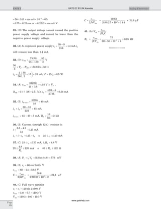
![[ ]z =
é
ë
ê
ê
ê
ù
û
ú
ú
ú
7
4
1
1
2
3
18. (D) Let I3 be the clockwise loop current in center
loop
I
V
I1
2
3
10
= + , V I I I V I2 2 3 3 2 24 0 25= + Þ = -( ) .
Þ = -I V I1 2 20 35. ...(i)
V I V V1 1 1 24 0 2= - +.
12 4 0 35 2 4 41 2 2 2 2 2. ( . ) .V V I V V I= - + = -
Þ = -V V I1 2 22 3 33. ...(ii)
19. (A) V I I
I
2 2 1
2
4
2
= + -
æ
è
ç
ö
ø
÷Þ = - +I I V2 1 22
1
2
...(ii)
I
I V V V
I
V V
V1
2 1 2 2
1
2 1
2
2 2 4 2
= +
- -
= - + + -
( )
Þ = +V I V1 1 24
3
2
...(i)
20. (B) I V
V V V
1 2
1 1 2
1 2
= - + +
-
= -
3
2
3
2
1 2V V ...(i)
I V
V V V
2 1
2 2 1
2
1 2
= + +
-
= +
3
2
3
2
1 2V V ...(ii)
21. (D) I V jV j V V1 1 1 1 22= + + -( )
Þ = + -I j V jV1 1 22 2( ) ...(i)
I
V
V j V V j V j V2
2
1 2 1 1 2
1
1 1= + + - = - + +( ) ( ) ( ) ...(ii)
22. (B) V
I
s
sI sI
s
s I sI1
1
1 2 1 2
1
= + + = +
æ
è
ç
ö
ø
÷ + ...(i)
V I s I sI2 2 2 12 2= + + Þ = + +V sI s I2 1 22 2( ) ...(ii)
23. (D) Z
n
R = = =
9 9
9
12
V I I1 1 14 1
4
5
= =( || ) Þ z
V
I
11
1
1
0 8= = .
V V nV I2 2 1 13
4
5
= ¢ = ¢ =
æ
è
ç
ö
ø
÷ Þ = =z
V
I
21
2
1
2 4. ,
¢ = =Z nR
2
4 36
V I I2 2 236 9 7 2= =( || ) . Þ z
V
I
22
2
2
7 2= = . ,
z z12 21 2 4= = .
24. (C) V sI sI sI sI sI1 1 1 1 1 23 3 3 3 2= + - + +
Þ = +V sI sI1 1 26 2 ...(i)
V sI sI2 2 13 2= + Þ = +V sI sI2 1 22 3 ...(ii)
25. (C) V
V
I1
2
2
5
0= + -( ), I V I1 2 20 5= + -( ) ( )
26. (A) V Z Z I Z Ia ab ab1 1 2= + +( ) ...(i)
V Z Z I Z I Z I Z Z Ia ab ab ab a ab2 2 1 1 2= + + = + +( ) ( ) ....(ii)
27. (A) I V V Y V Yab a1 1 2 1= - +( )
Þ = + -I V Y Y V Ya ab ab1 1 2( ) ...(i)
I V V Y V Y V Y V Y Yab b ab b ab2 2 1 2 1 2= - + = - + +( ) ( ) ...(ii)
28. (B) y-parameter of 1 W resistor network are
1 1
1 1
-
-
é
ë
ê
ù
û
ú
New y-parameter =
é
ë
ê
ù
û
ú +
5 3
1 2
1 1
1 1
6 2
0 3
-
-
é
ë
ê
ù
û
ú =
é
ë
ê
ù
û
ú.
29. (A) [ ]za =
2 0
0 10
1
mS
mS
é
ë
ê
ù
û
ú
-
=
é
ë
ê
ù
û
ú
5000 0
0 100
[ ]z =
é
ë
ê
ù
û
ú +
5000 0
0 100
100 100
100 100
é
ë
ê
ù
û
ú =
é
ë
ê
ù
û
ú
600 100
100 200
V I I1 1 2600 100= + , V I I2 1 2100 200= +
V I V I Is = + = +60 660 1001 1 1 2 , V V Io2 2300= = -
V I Vo o= -100
2
3
1 Þ I
Vo
1
60
=
V V
V
s o
o
= -11
3
Þ
V
V
o
5
3
32
=
30. (C) [ ]TN =
é
ë
ê
ù
û
ú
é
ë
ê
ù
û
ú =
é
ë
ê
ù
û
ú
2 1
1 1
2 1
1 1
5 3
3 2
V V I1 2 25 3= - , I V I1 2 23 2= -
Chap 1.10Two Port Networks
Page
99
I1
4 W V 2’
-
+
9 W
-
+
V2
I2=0
ZR
V1
1 : 3
-
+
V’1
Fig. S1.10.23a
V2
I2
4 W V 2’
-
+
9 W
-
+
V1
I =1 0
Z’R
1 : 3
-
+
V’1
Fig. S1.10.23b
GATE EC BY RK Kanodia
www.gatehelp.com](https://image.slidesharecdn.com/a-150815031147-lva1-app6892/85/A-gate-by-rk-kanodia-72-320.jpg)
![3 51 1 2V I I- = Þ V I I1 1 2
5
3
1
3
= + ...(i)
V I I2 1 2
1
3
2
3
= + ...(ii)
31. (B)
[ ]za =
é
ë
ê
ù
û
ú
3 1
1 2
, [ ]ya =
-
-
é
ë
ê
ê
ê
ù
û
ú
ú
ú
2
5
1
5
1
5
3
5
, [ ]yb =
-
-
é
ë
ê
ê
ê
ù
û
ú
ú
ú
3
2
1
2
1
2
5
2
[ ] [ ] [ ]y y ya b= + =
-
-
é
ë
ê
ê
ê
ù
û
ú
ú
ú
19
10
7
10
7
10
31
10
32. (D) [ ]ya =
3 2
2 4
s s
s s
-
-
é
ë
ê
ù
û
ú, [ ]yb =
3 0
2 4-
é
ë
ê
ù
û
ú
[ ] [ ] [ ]y y y
s s
s s
a b= = =
+ -
- - +
é
ë
ê
ù
û
ú
3 3 2
2 2 4 4
33. (C) h
I
I V
21
2
1 02
=
=
, - =
+
I
I R
R R
2
1
,
I
I
2
1
1
2
= -
34. (C)
I
V
y
V
2
1 0
21
2
1
10
0 1
=
= = = .
Interchanging the port
¢
¢
=
I
V
2
1
0 1. , ¢ = ´ =I2 100 0 1 10.
35. (B) For symmetrical network A D= = 3
For bilateral AD BC- = 1, 9 1 8- = =C C, S
36. (A) z
A
C
11
4
3
= =
37. (A) V V I I I aI1 1 1 1 2 10 5 2= + + + +. ( )
Þ = + +V a I I1 1 26 2 4( ) ...(i)
V I I aI2 1 2 12= + +( ) Þ = + +V a I I2 1 22 2( ) ...(ii)
For reciprocal network
z z12 21= , 4 2 2= + Þ =a a
38. (C) I V V1
3
1
3
24 10 0 1 10= ´ - ´ -
.
I V V2
3
1
3
250 10 10= ´ +- -
, V I2
3
210= -
- = ´ +- - -
10 50 10 103
2
3
1
3
2V V V , V V2 125= -
10 4 2 53
1 1 1I V V= + . ,
V
I
1
1
3
10
6 5
153 8= =
.
.
39. (B) I V V1
3
1
3
210 10 5 10= ´ - ´- -
,
100 25 1 1= +I V
100 0 25 0 1251 1 2- = -V V V. . Þ = -800 10 1 2V V ...(i)
I V V2
3
1
3
250 10 20 10= ´ + ´- -
, V I2 2100= -
V V V2 1 25 2= - - Þ 3 5 02 1V V+ = ...(ii)
From (i) and (ii) V V1 268 6 114 3= = -. , .V V.
40. (B) 100 5 20 21 1 1 1 2= + = +I V V I I,
Þ = +100 25 21 2I I , V I I2 1 240 10= +
800 5 342 2- = -V I Þ V I2 2160 6 8= + .
VTH = 160 V, RTH = 6 8. W
41. (B) V z I1 11 1= , V z I2 21 1= ,
V
V
z
z
2
1
21
11
=
42. (B) I y V y V2 21 1 22 2= + , I V YL2 2= -
y V y Y VL21 1 22 2 0+ + =( ) ,
V
V
y
y yL
2
1
21
22
=
-
+( )
43. (A) V z I z I2 21 1 22 2= + , V Z IL2 2= -
V z I z
V
ZL
2 21 1 22
2
= + -
æ
è
çç
ö
ø
÷÷
V Z z z Z IL L2 22 21 1( )+ = ,
V
I
z Z
z Z
L
L
2
1
21
22
=
+
**********
Page
100
UNIT 1 Networks
2 W 2 W1 W
1 W 1 W W
2
1
Fig. S.1.10.31a & b
2 F
2 F
2 F
Fig. S.1.10.32a
2V1
W
3
1 W
4
1
Fig. S.1.10.32b
R R
R
I1 I2
V1
+
-
Fig. S.1.10.33
GATE EC BY RK Kanodia
www.gatehelp.com](https://image.slidesharecdn.com/a-150815031147-lva1-app6892/85/A-gate-by-rk-kanodia-73-320.jpg)


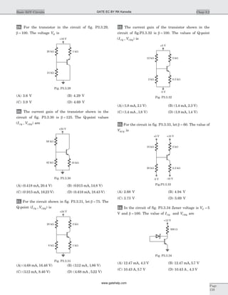


![VGS = 152. V, V VGS DS=
17. (B) I K V VD n GS TN= -( )2
Þ = -0 25 0 2 0 6 2
. . ( . )VGS Þ VGS = 172. V,
V V VGS G S= - , VG = 0, VS = -172. V
18. (A) I
V
R
D
D
D
=
-
=
5
0 8. mA, RD =
-
=
6 1
0 8
5
. m
kW
I K V VD n GS TN= -( )2
Þ 0 8 0 4 17 2
. ( . )( . )= -VGS Þ VGS = 311. V
V V VGS G S= - , VG = 0, VS = -311. V
I
R
D
S
= =
- - -
0 8
311 5
.
. ( )
mA Þ RS = 2 36. kW
19. (C) V VSD SG= , I
k W
L
V VD
p
GS TP=
¢
+
2
2
( )
10
25
2 4
2 5 154 2-
=
æ
è
ç
ö
ø
÷
æ
è
ç
ö
ø
÷ -
W
( . . ) Þ W = 32 mm
20. (D) Kp =
´æ
è
çç
ö
ø
÷÷ =
-
30 10
2
20 0 3
6
( ) . mA / V2
I K V VD p SG TP= +( )2
Þ 0 5 0 3 12 2
. . ( . )= -VSG
Þ =VSG 2 49. V, VG = 0
V VS SG= = 2 49. V
I
V
R
D
S
S
=
-5
Þ RS =
-
=
5 2 49
0 5
5 02
.
.
.
m
kW
I
V
R
D
D
D
=
- -( )5
Þ RD =
- +
=
3 5
0 5
4
. m
kW
21. (B) Assume transistor in saturation
I
V
K V VD
GS
n GS TN=
-
= -
10
10
2
k
( )
10 10 0 2 2 2
- = -V VGS GS( )( . )( )
Þ = -VGS 377 0 27. , .V V, VGS will be 3.77 V
V VGS DS= = 377. V
ID =
-
=
10 377
10
0 623
.
.
k
mA
Power = =I VD DS 2 35. mW
V V VDS GS TN> - assumption is correct.
22. (B) For both transistor V VDS GS= ,
V V VDS GS TN> - Therefore both transistor are in
saturation.
I ID D1 2= Þ K V V K V Vn GS TN n GS TN1 1 1
2
2 2 2
2
( ) ( )- = -
K K V Vn n TN TN1 2 1 2= =,
V VGS GS1 2
5
2
= = V
V Vo GS= =2 2 5. V
23. (A)
W
L
W
L
æ
è
ç
ö
ø
÷ >
æ
è
ç
ö
ø
÷
1 2
thus V VGS GS1 2<
40 0 8 15 0 81
2
2
2
( . ) ( . )V VGS GS- = -
V VGS GS2 15= -
1 63 0 8 5 0 81 1. ( . ) ( . )V VGS GS- = - -
VGS1 2 09= . , VGS 2 2 91= . V, V Vo GS= =2 2 91. V
24. (A) Each transistor is biased in saturation because
V VDS GS= and V V VDS GS TN> -
For M3 , V VGS2 32= =V
I
W
L
D = =
´æ
è
çç
ö
ø
÷÷
æ
è
ç
ö
ø
÷ -
-
0 5
36 10
2
2 1
3
3
2
. ( ) Þ
W
L
æ
è
ç
ö
ø
÷ =
3
27 8.
For M2 , V V VGS 2 1 2 5 2 3= - = - = V
I
W
L
D = =
´æ
è
çç
ö
ø
÷÷
æ
è
ç
ö
ø
÷ -
-
0 5
36 10
2
3 1
3
2
2
. ( ) Þ
W
L
æ
è
ç
ö
ø
÷ =
2
6 94.
For M1 , V VGS1 110 10 5 5= - = - = V
ID = = ´
æ
è
ç
ö
ø
÷
-
0 5
36
2
10 5
.
W
L
æ
è
ç
ö
ø
÷ -
1
2
5 1( ) Þ
W
L
æ
è
ç
ö
ø
÷ =
1
174.
25. (D) M2 is in saturation because
V V V VGS DS GS TN2 2 2= > -
M1 is in non saturation because
V VGS i1 5= = V, V VDS D1 0= = V
V V VDS GS TN1 1< - , I ID D1 2=
W
L
V V V VGS TN DS DS
æ
è
ç
ö
ø
÷ - -
1
1 1 1 2
2
2[ ( ) ]=
æ
è
ç
ö
ø
÷
W
L 2
( )V VGS TN2 2
2
-
Þ
W
L
æ
è
ç
ö
ø
÷ - - = - -
1
2 2
2 5 0 8 0 1 0 1 1 5 0 1 0 8[ ( . )( . ) ( . ) ] ( )( . . )
W
L
æ
è
ç
ö
ø
÷
1
( . ) .0 83 16 81= Þ
W
L
æ
è
ç
ö
ø
÷
1
=20.3
26. (B) I K V VD n GS TN1 1 1
2
= -( ) = -K V Vn GS TN2 2
2
( )
V VGS GS1 25= - Þ ( ) ( )5 1 200 12
2
2
2
- - = -V VGS GS
Þ VGS 2 2 76= . V, VGS1 2 24= . V
ID1
6 2
400 10 2 24 1= ´ --
( . ) =0.62 mA
27. (B) V VGS GS2 3 2 76= = . V
I K V V K V VD n GS TN n GS TN4 4 4
2
3 3
2
= - = -( ) ( )
= ´ --
100 10 2 76 16 2
( . ) = 0.31 mA
28. (C) V VGS DS= =4 2 0 1. , .V V
V V VDS GS TN< - , Thus transistor is in non saturation.
ID =
-
=
5 0 1
10
0 49
.
.
k
mA
{ }I
k W
L
V V V VD
n
GS TN DS DS=
¢
- -
2
2 2
( )
Chap 3.3Basic FET Circuits
Page
173
GATE EC BY RK Kanodia
www.gatehelp.com](https://image.slidesharecdn.com/a-150815031147-lva1-app6892/85/A-gate-by-rk-kanodia-122-320.jpg)
![RS = 4 kW, v vgs i= 0 84. ,
v g v r Ro m gs o D= - ( || )
= -( . )( . )( || )1 41 0 84 100 5m k kvi
Þ
v
v
Ao
i
v= = - 5 6.
28. (A) R R ro D o= || ||100k =4.76 kW
29. (A) As shown in fig. S3.4.27, R R Ri = =1 2 20 6|| . kW
30. (C) From the DC analysis:
VGSQ = 15. V, IDQ = 0 5. mA
g K V Vm n GS TN= -2 ( ) = - =2 1 15 0 8 1 4( ) ( . . ) .m mA V
r Io DQ= = ¥-
[ ]l 1
The resulting small-signal equivalent circuit is shown
in fig. S5.4.30
v g v Ro m gs D= - , v v g v Ri gs m gs S= +
Þ
v
v
g R
g R
o
i
m D
m S
=
-
+1
= -
+
( . )
( )
( . ) ( . )
1 4
7
1 1 4 0 5
m
k
m k
= -5 76.
31. (B) Since the DC gate current is zero, V VS GSQ= -
I I K V VDQ Q n GSQ TN= = -( )2
Þ 0 5 1 0 8 2
. ( . )= -VGSQ
V VGSQ S= = -151. V
VDSQ = - - - =5 0 5 7 151 301( . )( ) ( . ) .m k V
The transistor is therefore biased in the saturation
region. The small-signal equivalent circuit is shown in
fig.S3.4.31.
v g vo m gs= - ( )7k
v vgs i= ,
v
v
A go
i
v m= = - ( )7k
g K V Vm n GS TN= -2 ( )
= -2 1 151 0 8( )( . . )m = 1 42. mS
Av = - = -( . ) ( ) .1 42 7 9 9m k
32. (A) The small-signal equivalent circuit is shown in
fig. S.3.4.34
v g v R Ro m gs D L= - ( || ), v vi gs= -
A
v
v
g R Rv
o
i
m D L= = ( || ) = =( )( || ) .2 5 4 4 44m k k
33. (A) The small-signal equivalent circuit is shown in
fig. S3.4.33
v g v R ro m gs L o= ( || )
v v vi gs o= + = +v g v R rgs m gs L o( || )
v
g R r
gs
m L o
=
+
1
1 ( || )
v
v
A
g R r
g R r
o
i
v
m L o
m L o
= =
+
( || )
( || )1
R rL o|| ||= 4 100k k =
100
26
k
= 3 86. kW
Av =
+
=
( )( . )
( )( . )
.
2 3 85
1 2 3 85
0 89
m k
m k
34. (B) R
g
ro
m
o=
1
||
= æ
è
ç
ö
ø
÷
1
2
100||( ) » 0 498. kW
********************
Chap 3.4Amplifiers
Page
183
0.5 kW
7 kWRD
g vm gsvgs
+
_
G D
S
RTH
RS
vi
vo
~
Fig. S 3.4.30
vgs g vm gs
G D
S
vs
+
_
7 kW
vo
~
Fig. S3.4.31
500 kW ro
vo
4 kW
g vm gsvgs
+
_
G D
S
vi
~
Fig. S3.4.33
10 kW
vo
5 kW 4 kWvi
vgs
+
G
DS
g vm gs
RD RLRS
_
~
Fig. S3.4.32
GATE EC BY RK Kanodia
www.gatehelp.com](https://image.slidesharecdn.com/a-150815031147-lva1-app6892/85/A-gate-by-rk-kanodia-128-320.jpg)


![Duty cycle =
T
T
ON
=
-
5
6 6
2
p p
p
=
1
3
40.(A)
v v
R
v v
R
s o-
=
-- -
1 1
Þ 2 1v v vs o= +
v
R
v
R
v v
RL
o+ + +
+ +
-
=
2 2
0 Þ v
R
R
vo
L
= +
æ
è
çç
ö
ø
÷÷ +2 2
2 2 2
v v
R
R
vs
L
- += + +
æ
è
çç
ö
ø
÷÷ , v v- +=
Þ 0 2
= + +v
R
R
vs
L
v
R
R
vL
s+ = -
2
, i
v
R
L
L
= +
, i
v
R
L
s
= -
2
41. (D) This is a all pass circuit
v
v
H j
j RC
j RC
o
i
= =
-
+
( )w
w
w
1
1
, | |H j
R C
RC
( )
( )
( )
w
w
w
=
+
+
=
1
1
1
2 2
2
Thus when w and R is changed, the transfer function is
unchanged.
42. (B) Let R1 3= kW , R2 6= kW , C = 50 nF
v
R
sC
v v
R
i i o
1
2
1
0
||
æ
è
ç
ö
ø
÷
+
-
= Þ
v
R
sR C
v
R
v
R
i i o
1
1
2 2
1 +
æ
è
çç
ö
ø
÷÷
+ =
v
R
R
sR C vi o
2
1
11 1( )+ +
é
ë
ê
ù
û
ú =
[ ]
v
R
R R sR R C vi
o
1
2 1 1 2+ + =
v
v
R R
R
sR R C
R R
o
i
=
+
+
+
é
ë
ê
ù
û
ú
2 1
1
1 2
1 2
1
Þ ( )
v
v
R
R
s R R Co
i
= +
æ
è
çç
ö
ø
÷÷ +1 12
1
1 2( || )
f
R R C
dB3
1 2
1
2
=
p( || )
=
1
2 3 6 50p( || )k k n
= =
1
2 2 50
159
p( )
.
k n
kHz
43. (B) The oscillation frequency is
f
RC
=
1
2 6p
Þ 80
1
2 6 100
k =
p pR( )
Þ R = =
1
80 2 6 100
8 12
( )( )( )
.
k p p
kW
R
R
F
= 29 Þ RF = =( . )( )8 12 29 236k kW
44. (A) This is Wien-bridge oscillator. The ratio
R
R
2
1
2 1
1
2 1= =
.
.
k
k
is greater than 2. So there will be
oscillation
Frequency =
1
2pRC
Þ 1 10
1
2 1
3
´ =
p( )k C
C =
1
2p
mF
45. (C) v v vE+ -= = =5 V ,
The input current to the op-amp is zero.
i i iV Z C+ = +15 = +i iZ F Ea
=
-
+
æ
è
ç
ö
ø
÷ =
15 5
47
60
61
5
100
49 4
k
. mA
46. (B) v v vo o o= -
333
20
1 2( )
v v V
i
i
o BE t
c
s
1 1
1
= - -
æ
è
çç
ö
ø
÷÷ln , v v V
i
i
o BE t
c
s
2 2
2
= - -
æ
è
çç
ö
ø
÷÷ln
v v V
i
i
V
i
i
o o t
c
c
t
c
c
1 2
1
2
2
1
- = -
æ
è
çç
ö
ø
÷÷ =
æ
è
çç
ö
ø
÷÷ln ln
i
v
R
c1
1
1
= , i
v
R
c2
2
2
=
v v V
v
R
R
v
o o t1 2
2
2
1
1
- =
æ
è
çç
ö
ø
÷÷ln , Vt = 0 0259. V
v v v
v
v
R
R
o o o= - =
æ
è
çç
ö
ø
÷÷
333
20
333
20
0 02591 2
2
1
1
2
( ) ( . ) ln
=
æ
è
çç
ö
ø
÷÷0 4329 2
1
1
2
. ln
v
v
R
R
=
æ
è
çç
ö
ø
÷÷0 4329 2 3026 10
2
1
1
2
. ( . )log
v
v
R
R
=
æ
è
çç
ö
ø
÷÷log10
2
1
1
2
v
v
R
R
47. (B) v v+ -= , v
v v
Z
o o
=
+
=
10
10 30 4
v vo z= = ´ =4 6 2 4 24 8. . V
************
Page
194
UNIT 3 Analog Electronics
C
C
R
R
R2
R1
Fig. S3.5.44
GATE EC BY RK Kanodia
www.gatehelp.com](https://image.slidesharecdn.com/a-150815031147-lva1-app6892/85/A-gate-by-rk-kanodia-135-320.jpg)
![Statement for Q.39–40:
A Boolean function Z ABC= is to be implement
using NAND and NOR gate. Each gate has unit cost.
Only A, B and C are available.
39. If both gate are available then minimum cost is
(A) 2 units (B) 3 units
(C) 4 units (D) 6 units
40. If NAND gate are available then minimum cost is
(A) 2 units (B) 3 units
(C) 4 units (D) 6 units
41. In fig. P4.1.41 the LED emits light when
(A) both switch are closed
(B) both switch are open
(C) only one switch is closed
(D) LED does not emit light irrespective of the switch
positions
42. If the input to the digital circuit shown in fig.
P.4.1.42 consisting of a cascade of 20 XOR gates is X,
then the output Y is equal to
(A) X (B) X
(C) 0 (D) 1
43. A Boolean function of two variables x and y is
defined as follows :
f f f( , ) ( , ) ( , )0 0 0 1 1 1 1= = = ; f ( , )1 0 0=
Assuming complements of x and y are not
available, a minimum cost solution for realizing f using
2-input NOR gates and 2-input OR gates (each having
unit cost) would have a total cost of
(A) 1 units (B) 2 units
(C) 3 units (D) 4 units
44. The gates G1 and G2 in Fig. P.4.2.44 have
propagation delays of 10 ns and 20 ns respectively.
If the input Vi makes an abrupt change from logic
0 to 1 at t t= 0 then the output waveform Vo is
[t t1 0 10= + ns, t t2 1 10= + ns, t t3 2 10= + ns]
45. In the network of fig. P4.1.45 f can be written as
(A) X X X X X X X X X Xn n n0 1 3 5 2 4 5 1 1+ +- -.... ....
(B) X X X X X X X X X Xn n n0 1 3 5 2 3 4 1+ + -.... ....
(C) X X X X X X X X X X Xn n n n0 1 3 5 2 3 5 1.... ....+ + + -K
(D) X X X X X X X X X X X Xn n n n n0 1 3 5 1 2 3 5 1 2... ..- - -+ + + +K
*******
Chap 4.1Number Systems & Boolean Algebra
Page
201
t0 t1 t2 t3 t0 t1 t2 t3
t0 t1 t2 t3 t0 t1 t2 t3
(A)
(C)
(B)
(D)
VCC = 5 V
1 kW 1 kW 1 kW
1 kW
Fig. P4.1.41
1
X
Y
Fig. P4.1.42
1
Vi
0 Vi
G1
G2 Vo
to
Fig. P4.1.44
F
1
2
3
n
X1
X2
X3
Xn-1
Xn
X0
n-1
Fig. P4.1.45
GATE EC BY RK Kanodia
www.gatehelp.com](https://image.slidesharecdn.com/a-150815031147-lva1-app6892/85/A-gate-by-rk-kanodia-138-320.jpg)
![C C C3 2 1
* * *
= 110 which indicate position 6 in error
Transmitted code 1001100.
10. (D) X MNQ M NQ M NQ= + +
= +MQ M NQ = + = +Q M M N Q M N( ) ( )
11. (A) The logic circuit can be modified as shown in fig.
S. 4.1.11
Now Z AB C D E= + +( )
12. (D) You can see that input to last XNOR gate is
same. So output will be HIGH.
13. (D) Z A AB BC C= + + +( )
= + + + + +A A B B C C( ) = + +A B C
ABC A B C= + +
AB BC AC A B B C A C A B C+ + = + + + + + = + +
14. (C) ( )( )X Y X Y XY X Y+ + = +
( )( )( ) ( )( )X Y X Y X Y X Y XY X Y+ + + = + +
= + =XY XY XY
15. (B) Using duality
( )( )( ) ( )( )A B A C B C A B A C+ + + = + +
Thus (B) is correct option.
16. (B) Z AB CD EF= ( )( )( ) = + +AB CD EF
17. (A) X A B AB A B= + +( )( ) = + =( )( )AB A B AB AB
18. (B) Y A B C= Å ×( ) = + ×( )AB AC C
= + +( )AB AB C = + +A B AB C
19. (C) Z A A A BC ABC= + =( )
20. (A) Z AB B C ABC= + =( )
21. (A) Z A B BC AB BC ABC= + × = × =( ) ( )
22. (A) A A B A B C( )( )+ + +
= + + + = + + =( )( ) ( )AA AB A B C A A B C A
Therefore No gate is required to implement this
function.
23. (A)
A B C ( )A BC+ ( )( )A B A C+ +
0 0 0 0 0
0 0 1 0 0
0 1 0 0 0
0 1 1 1 1
1 0 0 1 1
1 0 1 1 1
Fig. S 4.1.23
24. (B) X ABC ABC ABC= + + = +BC ABC
25. (B) ( )( ) ( )( )A B B C AB BC ABC+ + = =
( )( ) ( ) ( )A B B C A B B C A B C+ + = + + + = + +
( )( ) ( ) ( )A B B C A B B C+ + = + + +
= + + = + +AB B C A B C
From truth table Z A B C= + +
Thus (B) is correct.
26. (D) AC BC AC B B A A BC+ = + + +( ) ( )
= + + +ABC ABC ABC ABC
27. (D) F A AB A BC A B C D DE= + + + +( )
= + + + +A AB A B C C D E( ( ))
= + + + +A A B B C D E( ( )) = + + + +A B C D E
28. (B) A B C AB AC AB AC AB AC( ( )) ( )+ + = + ×
= + + +AB AC A B A C[( )( )]
= + + + + =AB AC A AC AB B C AB( )
29. (C) ( ) ( )AB AB AB AB AB AB× = + = +
30. (B) X Z XZ X XY XY X X Y XY+ = + + +( ) ( )
= + + = + =X XY X Y XY XY XY Y( )
31. (A) X Y X Y XYÅ = + = + = = +( ) ( )XY XY XY X Y
Chap 4.1Number Systems & Boolean Algebra
Page
203
B
C D+
A
E
Z
Fig. S4.1.11
GATE EC BY RK Kanodia
www.gatehelp.com](https://image.slidesharecdn.com/a-150815031147-lva1-app6892/85/A-gate-by-rk-kanodia-140-320.jpg)


![30. y t u t h t( ) ( ) * ( )= , where h t
e t
e t
t
t
( )
,
,
=
<
>
ì
í
î
-
2
3
0
0
(A)
1
2
1
5
6
1
3
2 3
e u t e u tt t- -
- - + - -( ) ( )
(B)
1
2
1
5
6
1
3
2 3
e u t e u tt t
( ) ( )- - + - --
(C)
1
2
1
6
5 3 22 2 3
e e e u tt t t
+ - - -
[ ] ( )
(D)
1
2
1
6
5 3 22 2 3
e e e u tt t t
+ - - --
[ ] ( )
Statement for Q.31-34:
The impulse response of LTI system is given.
Determine the step response.
31. h t e t
( ) | |
= -
(A) 2 + - -
e et t
(B) e u t et t
( )- + + - -
1 2
(C) e u t e u tt t
( ) [ ] ( )- + + - -
1 2 (D) e e e u tt t t
+ - --
[ ] ( )2
32. h t t( ) ( )( )
= d 2
(A) 1 (B) u t( )
(C) d( )
( )3
t (D) d( )t
33. h t u t u t( ) ( ) ( )= - - 4
(A) tu t t u t( ) ( ) ( )+ - -1 4 (B) tu t t u t( ) ( ) ( )+ - -1 4
(C) 1 + t (D) ( ) ( )1 + t u t
34. h t y t( ) ( )=
(A) u t( ) (B) t
(C) 1 (D) tu t( )
Statement for Q.35-38:
The system described by the differential equations
has been specified with initial condition. Determine the
output of the system and choose correct option.
35.
dy t
dx
y t x t
( )
( ) ( )+ =10 2 , y x t u t( ) , ( ) ( )0 1-
= =
(A) 1
5
10
1 4( ) ( )+ -
e u tt
(B) 1
5
10
1 4( )+ -
e t
(C) - + -1
5
10
1 4( ) ( )e u tt
(D) - + -1
5
10
1 4( )e t
36.
d y t
dt
dy t
dt
y t
dx t
dt
2
2
5 4
( ) ( )
( )
( )
+ + = ,
y ( )0 0-
= ,
dy t
dt
( )
0
1
-
= , x t t u t( ) sin ( )=
(A)
5
34
3
34
1
6
13
61
4
sin cost t e et t
+ + -- -
, t ³ 0
(B)
5
34
3
34
13
51
1
6
4
sin cost t e et t
+ - +- -
, t ³ 0
(C)
3
34
5
34
13
51
1
6
4
sin cost t e et t
+ - +- -
, t ³ 0
(D)
3
34
5
34
1
6
13
51
4 4
sin cost t e et t
+ + -- -
, t ³ 0
37.
d y t
dt
dy t
dt
y t x t
2
2
6 8 2
( ) ( )
( ) ( )+ + = ,
y ( ) ,0 1-
= -
dy t
dt
( )
0
1
-
= , x t e u tt
( ) ( )= -
(A)
2
3
5
2
5
6
2 4
e e et t t- - -
- + , t ³ 0
(B)
2
3
5
2
5
6
2 4
+ +- -
e et t
, t ³ 0
(C) 4 5 3 2 4
+ +- -
( )e et t
, t ³ 0
(D) 4 5 3 2 4
- +- -
( )e et t
, t ³ 0
38.
d y t
dt
y t
dx t
dt
2
2
3( )
( )
( )
+ = ,
y ( ) ,0 1-
= -
dy t
dt
( )
0
1
-
= , x t te u tt
( ) ( )= -
2
(A) sin cost t te tt
+ - +-
4 3 3
, t ³ 0
(B) 4 3sin cost t te t
- - -
, t ³ 0
(C) sin cost t te tt
- + +-
4 3 3
, t ³ 0
(D) 4 3sin cost t te t
+ - -
, t ³ 0
39. The raised cosine pulse x t( ) is defined as
x t
t t
( )
(cos ) ,
,
=
+ - £ £
ì
í
ï
îï
1
2
1
0
w
p
w
p
w
otherwise
The total energy of x t( ) is
(A)
3
4
p
w
(B)
3
8
p
w
(C)
3p
w
(D)
3
2
p
w
40. The sinusoidal signal x t t( ) cos ( )= +4 200 6p is
passed through a square law device defined by the
input output relation y t x t( ) ( )= 2
. The DC component in
the signal is
(A) 3.46 (B) 4
(C) 2.83 (D) 8
Page
252
UNIT 5 Signal & SystemGATE EC BY RK Kanodia
www.gatehelp.com](https://image.slidesharecdn.com/a-150815031147-lva1-app6892/85/A-gate-by-rk-kanodia-165-320.jpg)
![At time, t y x x= = - -0 0 5 3, ( ) ( ) ( ). Therefore the
response at time, t = 0 depends on the excitation at a
later time t = 3. (Not causal)
If x t( ) is bounded then x t( )- 5 and x t( )3 - are bounded
and so is y t( ). (Stable)
18. (D) y t v
t
y t kv
t
ky t1 2 1
2 2
( ) , ( ) ( )=
æ
è
ç
ö
ø
÷ =
æ
è
ç
ö
ø
÷ =
(Homogeneous)
x v t w t3 = +( ) ( ) then
y t v
t
w
t
y y y t3 1 2
2 2
( ) ( ) ( )=
æ
è
ç
ö
ø
÷ +
æ
è
ç
ö
ø
÷ = + (Additive)
Since it is both homogeneous and additive, it is also
linear
y t v
t
1
2
( ) =
æ
è
ç
ö
ø
÷ , y
t
t y t t v
t t
o o
o
2
2 2
-
æ
è
ç
ö
ø
÷ ¹ - =
-æ
è
ç
ö
ø
÷( )
(Time variant)
At time t y x= - - = -2 2 1, ( ) ( ), therefore, the response at
time t = -2, depends on the excitation at a later time,
t = -1. (Not causal)
It x t( ) is bounded then y t( ) is bounded. (Stable)
19. (C) y t t v t1 2( ) cos ( )= p
y t k t v t ky t2 12( ) cos ( ) ( )p = (Homogeneous)
x t v t w t3( ) ( ) ( )= +
y t t v t w t y t y t3 1 22( ) cos [ ( ) ( )] ( ) ( )= + = +p (Additive)
Since it is both homogeneous and additive. It is also
linear.
y t t v t1 2( ) cos ( )= p
y t t t t y t to o2 2( ) cos ( ) ( )= - ¹ -p
= - -cos [ ( )] ( )2p t t v t to o (Time Variant)
The response at any time t to= depends only on the
excitation at that time and not on the excitation at any
later time. (Causal)
If x t( ) is bounded then y t( ) is bounded. (Stable)
20. (C) | |y t v t1( ) ( )= , | |y t kv t k y t2 1( ) ( ) ( )= =
If k is negative k y t1( ) ¹ ky t1( )
(Not Homogeneous Not linear).
| |y t v t1( ) ( )= , | |y t y t t y t to o2 1( ) ( ) ( )= - = -
(Time Invariant)
The response at any time t to= depends only on the
excitation at that time and not on the excitation at any
later time. (Causal)
If x t( ) is bounded then y t( ) is bounded. (Stable)
21. (C) All option are linear. So it is not required
to check linearity.
Let x t v t1( ) ( )= then t
d
dt
y t y t v t1 18( ) ( ) ( )- =
Let x t v t to2( ) ( )= - then t
d
dt
y t y t v t to2 28( ) ( ) ( )- = -
The first equation can be written as
( ) ( ) ( ) ( )t t
d
dt
y t t y t t v t to o o o- - - - = -8
This equation is not satisfied if y t y t to2 1( ) ( )= - therefore
y t y t to2 1( ) ( )¹ - (Time Variant)
The system can be written as
y t
x
d
y
d
t t
( )
( ) ( )
= +
-¥ -¥
ò ò
l
l
l
l
l
l8
So the response at any time, t to= depends on the
excitation at t to£ , and not on any future values.
(Causal)
The Homogeneous solution to the differential equation
is of the form y t kt( ) = 8
. If there is no excitation but the
zero excitation, response is not zero. The response will
increases without bound as time increases.
(Unstable)
22. (C) y t v d
t
1
3
( ) (=
-¥
+
ò l) l
y t kv d k v d ky t
t t
2
3 3
1( ) ( ( ( )= =
-¥
+
-¥
+
ò òl) l l) l = (Homogeneous)
x t v t w t3( ) ( ) ( )= +
y t v w d v d w d
t t t
3
3 3 3
( ) [ ( ) ( )] ( ) ( )= + = +
-¥
+
-¥
+
-¥
+
ò ò òl l l l l l l
= +y (t) y (t)1 2 (Additive)
Since it is Homogeneous and additive, it is also linear.
y t v d
t
1
3
( ) (=
-¥
+
ò l) l
y t v t d v d y (t t
t t t
2
3 3
1( ) ( ( )= =
-¥
+
-¥
+
ò òl - ) l = l) l -
-
o o
o
(Time invariant)
The response at any time, t t= o , depends partially on
the excitation at time to t t to o< < +( )3 which are in
future. (Not causal)
If x t( ) is a constant k, then y t kd k d
t t
( ) = =
-¥
+
-¥
+
ò ò
3 3
l l and as
t y t® ¥ , ( ) increases without bound. (unstable)
Chap 5.1Continuous-Time Systems
Page
255
GATE EC BY RK Kanodia
www.gatehelp.com](https://image.slidesharecdn.com/a-150815031147-lva1-app6892/85/A-gate-by-rk-kanodia-168-320.jpg)
![11. x n y n[ ] [ ]+ -2 2
Statement for Q.12–15:
A discrete-time signal is given. Determine the
period of signal and choose correct option.
12. x n
n n
[ ] cos sin= + +
æ
è
ç
ö
ø
÷
p p
9 7
1
2
(A) periodic with period N = 126
(B) periodic with period N = 32
(C) periodic with period N = 252
(D) Not periodic
13. x n
n n
[ ] cos cos=
æ
è
ç
ö
ø
÷
æ
è
ç
ö
ø
÷
8 8
p
(A) Periodic with period 16p
(B) periodic with period 16 1( )p +
(C) periodic with period 8
(D) Not periodic
14. x n
n n n
[ ] cos sin cos=
æ
è
ç
ö
ø
÷ -
æ
è
ç
ö
ø
÷ + +
æ
è
ç
ö
ø
÷
p p p p
2 8
3
4 3
(A) periodic with period 16
(B) periodic with period 4
(C) periodic with period 2
(D) Not periodic
15. x n e
j
n
[ ] =
-
æ
è
çç
ö
ø
÷÷
2 6
p
(A) periodic with 12p (B) periodic with 12
(C) periodic with 11p (D) Not periodic
16. The sinusoidal signal has fundamental period
N = 10 samples. The smallest angular frequency, for
which x n[ ] is periodic, is
(A)
1
10
rad/cycle (B) 10 rad/cycle
(C) 5 rad/cycle (D)
p
5
rad/cycle
17. Let x n n[ ], - £ £5 3 and h n n[ ], 2 6£ £ be two finite
duration signals. The range of their convolution is
(A) - £ £7 9n (B) - £ £3 9n
(C) 2 3£ £n (D) - £ £5 6n
Statement for Q.18–26:
x n[ ] and h n[ ] are given in the question. Compute
the convolution y n x n h n[ ] [ ]* [ ]= and choose correct
option.
18. x n[ ] = {1, 2, 4}, h n[ ] = {1, 1, 1, 1, 1}
(A) {1, 3, 7, 7, 7, 6, 4}
(B) {1, 3, 3, 7, 7, 6, 4}
(C) {1, 2, 4}
(D) {1, 3, 7}
19. x n[ ] = {1, 2, 3, 4, 5}, h n[ ] = {1}
(A) {1, 3, 6, 10, 15} (B) {1, 2, 3, 4, 5}
(C) {1, 4, 9, 16, 20} (D) {1, 4, 6, 8, 10}
20. x n[ ] = {1, 2, -1}, h n x n[ ] [ ]=
(A) {1, 4, 1} (B) {1, 4, 2, -4, 1}
(C) {1, 2, -1} (D) {2, 4, -2}
Page
260
UNIT 5 Signal & System
2
3
1
x n[ ]
n
2 31 4 5 60-1-2-3-4-5-6
(A)
2
3
1
x n[ ]
n
2 31 4 5 60-1-2-3-4-5-6
(B)
-2
-3
-1
n
2 31 4 5 6-1-2-3-4-5-6
(C)
-2
-3
-1
n
2 31 4 5 6-1-2-3-4-5-6
(D)
GATE EC BY RK Kanodia
www.gatehelp.com](https://image.slidesharecdn.com/a-150815031147-lva1-app6892/85/A-gate-by-rk-kanodia-169-320.jpg)
![21. x n[ ] = {1, -2, 3}, h n[ ] = {0, 0, 1, 1, 1, 1}
(A) {1, -2, 4, 1, 1, 1}
(B) {0, 0, 3}
(C) {0, 0, 3, 1, 1, 1, 1}
(D) {0, 0, 1, -1, 2, 2, 1, 3}
22. x n[ ] = {0, 0, 1, 1, 1, 1}, h n[ ] = {1, -2, 3}
(A) {0, 0, 1, -1, 2, 2, 1, 3}
(B) {0, 0, 1, -1, 2, 2, 1, 3}
(C) {1, -2, 3, 1, 1, 2, 1, 1}
(D) {1, -2, 3, 1, 1, 1, 1}
23. x n[ ] = {1, 1, 0, 1, 1}, h n[ ] = {1, - -2 3, , 4}
(A) {1, - -1 2, , 4, 1, 1}
(B) {1, - -1 2, , 4, 1, 1}
(C) {1, - -1 5, , 2, 3, -5, 1, 4}
(D) {1, - -1 5, , 2, 3, -5, 1, 4}
24. x n[ ] = {1, 2, 0, 2, 1}, h n x n[ ] [ ]=
(A) {1, 4, 4, 4, 10, 4, 4, 4, 1}
(B) {1, 4, 4, 4, 10, 4, 4, 4, 1}
(C) {1, 4, 4, 10, 4, 4, 4, 1}
(D) {1, 4, 4, 10, 4, 4, 4, 1}
25. x n[ ] = {1, 4, -3, 6, 4}, h n[ ] = {2, -4, 3}
(A) {2, 4, -19, 36, -25, 2, 12}
(B) {4, -19, 36, -25}
(C) {1, 4, -3, 6, 4}
(D) {1, 4, -3, 6, 4}
26. x n
n
n[ ]
, , ,
,=
= -
= -
ì
í
ï
î
ï
1 2 0 1
2 1
0 elsewhere
h n n n n( ) [ ] [ ] [ ]= - - + -d d d1 4
(A) d d d d[ ] [ ] [ ] [ ]n n n n- - + - + -2 1 4 4 5
(B) d d d d d d[ ] [ ] [ ] [ ] [ ] [ ]n n n n n n+ + + - + - + - + -2 1 2 3 4 5
(C) d d d d d d[ ] [ ] [ ] [ ] [ ] [ ]n n n n n n+ - + + + - - - + -2 1 2 3 4 2 5
(D) d d d d[ ] [ ] [ ] [ ]n n n n+ - + - + -2 1 4 5 5
Statement for Q.27–30:
In question y n[ ] is the convolution of two signal.
Choose correct option for y n[ ].
27. y n u nn n
[ ] ( ) * [ ]= - +1 2 2 2
(A)
4
6
(B)
4
6
2u n[ ]- +
(C)
8
3
1 2( ) [ ]- - +n
u n (D)
8
3
1( )- n
28. y n u n u nn
[ ] [ ]* [ ]= +
1
4
2
(A)
1
3
1
4
-
æ
è
ç
ö
ø
÷n
u n[ ] (B)
1
3
12
4
2-
æ
è
ç
ö
ø
÷ +n
u n[ ]
(C)
4
3
1
12
1
4
2-
æ
è
ç
ö
ø
÷
æ
è
ç
ç
ö
ø
÷
÷
+
n
u n[ ] (D)
16
3
1
4
2-
æ
è
ç
ö
ø
÷ +n
u n[ ]
29. y n u n u nn
[ ] [ ]* [ ]= - + -3 3 2
(A)
3
2
5
83
2
6
n
n
n
,
,
£
³
ì
í
ïï
î
ï
ï
(B)
3 5
83
2
6
n
n
n
,
,
£
³
ì
í
ï
îï
(C)
3
2
5
81
2
6
n
n
n
,
,
£
³
ì
í
ïï
î
ï
ï
(D)
3
6
5
81
2
6
n
n
n
,
,
£
³
ì
í
ïï
î
ï
ï
Chap 5.2Discrete-Time Systems
Page
261
GATE EC BY RK Kanodia
www.gatehelp.com](https://image.slidesharecdn.com/a-150815031147-lva1-app6892/85/A-gate-by-rk-kanodia-170-320.jpg)
![30. y n u n u n[ ] [ ]* [ ]= + -3 3
(A) ( ) [ ]n u n+ 1 (B) nu n[ ]
(C) ( ) [ ]n u n- 1 (D) u n[ ]
31. The convolution of x n n u n[ ] cos ( ) [ ]= p
2
and
h n u n[ ] [ ]= - 1 is f n u n[ ] [ ]- 1 . The function f n[ ] is
(A)
1 4 1 4 2
0 4 4 3
, ,
, ,
n m m
n m m
= + +
= +
ì
í
î
(B)
0 4 1 4 2
1 4 4 3
, ,
, ,
n m m
n m m
= + +
= +
ì
í
î
(C)
1 4 1 4 3
0 4 4 2
, ,
, ,
n m m
n m m
= + +
= +
ì
í
î
(D)
0 4 1 4 3
1 4 4 2
, ,
, ,
n m m
n m m
= + +
= +
ì
í
î
Statement for Q.32–38:
Let P be linearity, Q be time invariance, R be
causality and S be stability. In question discrete time
input x n[ ] and output y n[ ] relationship has been given. In
the option properties of system has been given. Choose
the option which match the properties for system.
32. y n rect x n[ ] ( [ ])=
(A) P, Q, R (B) Q, R, S
(C) R, S, P (D) S , P, Q
33. y n nx n[ ] [ ]=
(A) P, Q, R, S (B) Q, R, S
(C) P, R (D) Q, S
34. y n u m
m
n
[ ] [ ]=
=-¥
+
å
1
(A) P, Q, R, S (B) R, S
(C) P, Q (D) Q, R
35. y n x n[ ] [ ]=
(A) Q, R, S (B) R, S, P
(C) S, P, Q (D) P, Q, R
36. x n[ ] as shown in fig. P5.2.36
(A) P, Q, R, S (B) Q, R, S
(C) P, Q (D) R, S
37. x n[ ] as shown in fig. P5.2.37
(A) P, Q, R, S (B) Q, R, S
(C) P, R, S (D) P, Q, S
38. x n[ ] as shown in fig. P5.2.38
(A) P, Q, R, S (B) P, Q, R
(C) P, Q (D) Q, R, S
Statement for Q.39–41:
Two discrete time systems S1 and S2 are
connected in cascade to form a new system as shown in
fig. P5.2.39–41.
39. Consider the following statements
(a) If S1 and S2 are linear, the S is linear
(b) If S1 and S2 are nonlinear, then S is nonlinear
(c) If S1 and S2 are causal, then S is causal
(d) If S1 and S2 are time invariant, then S is time
invariant
True statements are :
(A) a, b, c (B) b, c, d
(C) a, c, d (D) All
40. Consider the following statements
(a) If S1 and S2 are linear and time invariant, then
interchanging their order does not change the system.
(b) If S1 and S2 are linear and time varying, then
interchanging their order does not change the system.
True statement are
(A) Both a and b (B) Only a
(C) Only b (D) None
Page
262
UNIT 5 Signal & System
2x n[ ] y n[ ]
Fig. P5.2.36
+
5
10x n[ ] y n[ ]
Fig. P5.2.37
+
+
x n[ ] y n[ ]
Fig. P5.2.38
S1
S2x n[ ] y n[ ]
Fig. P5.2.39–41.
GATE EC BY RK Kanodia
www.gatehelp.com](https://image.slidesharecdn.com/a-150815031147-lva1-app6892/85/A-gate-by-rk-kanodia-171-320.jpg)
![41. Consider the statement
(a) If S1 and S2 are noncausal, the S is non causal
(b) If S1 and/or S2 are unstable, the S is unstable.
True statement are :
(A) Both a and b (B) Only a
(C) Only b (D) None
42. The following input output pairs have been
observed during the operation of a time invariant
system :
x n y n
x n y
S
S
1 1
2
1 0 2 0 1 2
0 0 3
[ ] { , , } [ ] { , , }
[ ] { , , }
= ¬ ®¾ =
= ¬ ®¾ 2
3 3
0 1 0 2
0 0 0 1 1 2 1
[ ] { , , , }
[ ] { , , , } [ ] { , , }
n
x n y nS
=
= ¬ ®¾ =
The conclusion regarding the linearity of the
system is
(A) System is linear
(B) System is not linear
(C) One more observation is required.
(D) Conclusion cannot be drawn from observation.
43. The following input output pair have been observed
during the operation of a linear system:
x n y n
x n
S
1 1
2
1 2 1 1 2 1 0 1
1 1
[ ] { , , } [ ] { , , , , }
[ ] { , ,
= - ¬ ®¾ = -
= - - ¬ ®¾ = -
= ¬ ®¾ =
1 1 1 0 2
0 1 1 1
2
3 3
} [ ] { , , , }
[ ] { , , } [ ] {
S
S
y n
x n y n , , }2 1
The conclusion regarding the time invariance of
the system is
(A) System is time-invariant
(B) System is time variant
(C) One more observation is required
(D) Conclusion cannot be drawn from observation
44. The stable system is
(A) y n x n y n[ ] [ ] . [ ]= + -11 1
(B) y n x n y n y n[ ] [ ] ( [ ] [ ])= - - + -
1
2
1 2
(C) y n x n y n y n[ ] [ ] ( . [ ] . [ ])= - - + -15 1 0 4 2
(D) Above all
45. The system shown in fig. P5.2.45 is
(A) Stable and causal
(B) Stable but not causal
(C) Causal but unstable
(D) unstable and not causal
46. The impulse response of a LTI system is given as
h n u n
n
[ ] [ ]= -
æ
è
ç
ö
ø
÷
1
2
.
The step response is
(A)
1
3
2
1
2
1
- -
æ
è
ç
ö
ø
÷
æ
è
ç
ç
ö
ø
÷
÷
+n
u n[ ] (B)
1
3
2
1
2
- -
æ
è
ç
ö
ø
÷
æ
è
ç
ç
ö
ø
÷
÷
n
u n[ ]
(C)
1
3
2
1
2
1
+ -
æ
è
ç
ö
ø
÷
æ
è
ç
ç
ö
ø
÷
÷
+n
u n[ ] (D)
1
3
2
1
2
+ -
æ
è
ç
ö
ø
÷
æ
è
ç
ç
ö
ø
÷
÷
n
u n[ ]
47. The difference equation representation for a system
is
y n y n x n[ ] [ ] [ ]- - =
1
2
1 2 , y [ ]- =1 3
The natural response of system is
(A)
3
2
1
2
-
æ
è
ç
ö
ø
÷
n
u n[ ] (B)
2
3
1
2
-
æ
è
ç
ö
ø
÷
n
u n[ ]
(C)
3
2
1
2
æ
è
ç
ö
ø
÷
n
u n[ ] (D)
2
3
1
2
æ
è
ç
ö
ø
÷
n
u n[ ]
48. The difference equation representation for a system is
y n y n y n x n x n[ ] [ ] [ ] [ ] [ ]- - + - = - -2 1 2 1
If y n[ ] = 0 for n < 0 and x n n[ ] [ ]= d , then y[ ]2 will
be
(A) 2 (B) -2
(C) -1 (D) 0
49. Consider a discrete-time system S whose response
to a complex exponential input ej np 2
is specified as
S e ej n j n
: p p2 3 2
Þ
Chap 5.2Discrete-Time Systems
Page
263
+
+
+
+
x n[ ] D
y n[ ]
y n-2[ ]D
-1
2
1
4
1
4
Fig. P5.2.45
GATE EC BY RK Kanodia
www.gatehelp.com](https://image.slidesharecdn.com/a-150815031147-lva1-app6892/85/A-gate-by-rk-kanodia-172-320.jpg)
![24. (B) y n[ ] = {1, 4, 4, 10, 4, 4, 4, 1}
25. (A) y n[ ] = {2, 4, -19, 36, -25, 2, 12}
26. (B) x n[ ] = {1, 2, 1, 1}, h n[ ] = {1, -1, 0, 0, 1}
y n[ ] = {1, 1, -1, 0, 0, 2, 1, 1}
y n n n n n n n[ ] [ ] [ ] [ ] [ ] [ ] [ ]= + + + - + - + - + -d d d d d d2 1 2 3 4 5
27. (D) y n k n k
k n
[ ] ( )= - -
= -
¥
å 1 2
2
= -
æ
è
ç
ö
ø
÷
= -
¥
å2
1
22
n
k
k n
=
-
æ
è
ç
ö
ø
÷
+
-
2
1
2
1
1
2
2
n
n
= -
8
3
1( )n
28. (C) For n n+ < < -2 0 2or , y n[ ] = 0
for n n+ ³ ³ -2 0 2or , y n k
k
n
[ ] =
=
+
å
1
40
2
= -
4
3
1
12
1
4n
,
Þ = -
æ
è
ç
ö
ø
÷
æ
è
ç
ç
ö
ø
÷
÷
+y n u n
n
[ ] [ ]
4
3
1
12
1
4
2
29. (D) For n n- £ £2 3 5or , y n k
k
n n
[ ] = =
=¥
-
å3
3
6
2
for n n- ³ ³2 4 6or , y n k
k
[ ] = =
=-¥
å3
81
2
3
,
Þ =
£
³
ì
í
ïï
î
ï
ï
y n
n
n
n
[ ]
,
,
3
6
5
81
2
6
30. (A) For n - < -3 3 or n < 0, y n[ ] = 0
for n n- ³ - >3 3 0or , y n n
k
n
[ ] = = +
=-
-
å 1 1
3
3
,
y n n u n[ ] ( ) [ ]= + 1
31. (A) For n n- < <1 0 1or , y n[ ] = 0
For n n- ³ ³1 0 1or , y n k
k
n
[ ] cos=
æ
è
ç
ö
ø
÷
=
-
å
p
20
1
Þ =
= + +
= +
ì
í
î
y n
n m m
n m m
[ ]
, ,
, ,
1 4 1 4 2
0 4 4 3
32. (B) y n rect v n1[ ] ( [ ])= , y n rect kv n2[ ] ( [ ])=
y n k y n2 1[ ] [ ]¹ (Not Homogeneous not linear)
y n rect v n y n rect v n no1 2[ ] ( [ ]), [ ] ( [ ])= = -
y n n rect v n n y no o1 2[ ] ( [ ]) [ ]- = - = (Time Invariant)
At any discrete time n no= , the response depends only
on the excitation at that discrete time. (Causal)
No matter what values the excitation may have the
response can only have the values zero or one.
(Stable)
33. (C) y n nv n y n nkv n1 2[ ] [ ], [ ] [ ]= =
ky n y n1 2[ ] [ ]= (Homogeneous)
Let x n v n1[ ] [ ]= then y n nv n1[ ] [ ]=
Let x n w n2[ ] [ ]= then y n nw n2[ ] [ ]=
Let x n v n w n3[ ] [ ] [ ]= + then
y n n v n w n nv n nw n3[ ] ( [ ] [ ]) [ ] [ ]= + = +
= +y n y n1 2[ ] [ ] (Additive)
Since the system is homogeneous and additive, it is also
linear.
y n n n n v n n y n nv n no o o n o1[ ] ( ) [ ] [ ] [ ]- = - - ¹ = -
Page
266
UNIT 5 Signal & System
1
22
4 -3 6 4
8 -6 12 8
-4 -16 12 -24 -16-4
3 12 -9 18 123
Fig. S5.2.25
1
11
2 1 1
2 1 -1
-1 -2 -1 -1-1
0 0 0 00
0 0 0 00
1 2 1 11
Fig. S5.2.26
1
11
2 0 2 1
2 0 2 1
2 4 0 4 22
0 0 0 0 00
2 4 0 4 22
1 2 0 2 11
Fig. S5.2.24
GATE EC BY RK Kanodia
www.gatehelp.com](https://image.slidesharecdn.com/a-150815031147-lva1-app6892/85/A-gate-by-rk-kanodia-173-320.jpg)
![(Time variant)
At any discrete time, n no= the response depends only
on the excitation at that same time. (Causal)
If the excitation is a constant, the response is
unbounded as n approaches infinity. (Unstable)
34. (C) y n v m y n kv m
m
n
m
n
1
1
2
1
[ ] [ ] , [ ] [ ]= =
=-¥
+
=-¥
+
å å
y n ky n2 1[ ] [ ]= (Homogeneous)
y n v m
n
n
1
1
[ ] [ ],=
=-¥
+
å y n w m
n
n
2
1
[ ] [ ]=
=-¥
+
å
y n v n w m
m
n
3
1
[ ] ( [ ] [ ])= +
=-¥
+
å
= + = +
=-¥
+
=-¥
+
å åv m w n y n y n
m
n
m
n
[ ] [ ] [ ] [ ]
1 1
1 2 (Additive)
Since the system is homogeneous and additive it is also
linear
y n v n y n v m n
m
n
o
m
n
1
1
2
1
[ ] [ ] , [ ] [ ]= = -
=-¥
+
=-¥
+
å å
y n n v m v q n y no
m
n n
o
q
no
1
1 1
2[ ] [ ] [ ] [ ]- = = - =
=-¥
- +
=-¥
+
å å
(Time Invariant)
At any discrete time, n no= , the response depends on
the excitation at the next discrete time in future.
(Anti causal)
If the excitation is a constant, the response increases
without bound. (Unstable)
35. (A) y n v n y kv n k v n1 2[ ] [ ] , [ ] [ ]= = =
ky n k v n y n1 2[ ] [ ] [ ]= ¹ (Not Homogeneous Not linear)
y n v n y n v n no1 2[ ] [ ] , [ ] [ ]= = -
y n n v n n y no o1 2[ ] [ ] [ ]- = - = (Time Invariant)
At any discrete time n no= , the response depends only
on the excitation at that time (Causal)
If the excitation is bounded, the response is bounded.
(Stable).
36. (B) y n x n[ ] [ ]= 2 2
Let x n v n1[ ] [ ]= then y n v n1
2
2[ ] [ ]=
Let x n kv n2[ ] [ ]= then y n k v n2
2 2
2[ ] [ ]=
ky n y n[ ] [ ]¹ 2 (Not homogeneous Not linear)
Let x n v n1[ ] [ ]= then y n v n1
2
2[ ] [ ]=
Let x n v n no2[ ] [ ]= - then y n v n no2
2
2[ ] [ ]= -
y n n v n n y no o1 22[ ] [ ] [ ]- = - = (Time invariant)
At any discrete time, n no= , the response depends only
on the excitation at that time. (Causal)
If the excitation is bounded, the response is bounded.
(Stable).
37. (B) y n v n1 10 5[ ] [ ]= - , y n kv n2 10 5[ ] [ ]= -
y n ky n2 1[ ] [ ]¹ (Not Homogeneous so not linear)
y n v n y n v n no1 210 5 10 5[ ] [ ] , [ ] [ ]= - = - -
y n n v n n y no o1 210 5[ ] [ ] , [ ]- = - - = (Time Invariant)
At any discrete time, n no= the response depends only
on the excitation at that discrete time and not on any
future excitation. (Causal)
If the excitation is bounded, the response is bounded.
(Stable).
38. (B) y n x n y n[ ] [ ] [ ]= + - 1 , y n x n y n[ ] [ ] [ ]- = - + -1 1 2
y n x n x n y n[ ] [ ] [ ] [ ]= + - + -1 2 , Then by induction
y n x n x n x n k[ ] [ ] [ ] [ ]= - + - + - +1 2 K K = -
=
¥
å x n k
k
[ ]
0
Let m n k= - then y n x m x m
m n m
n
[ ] [ ] [ ]= =
=
-¥
=-¥
å å
y n v m y n kv m ky n
m
n
m
n
1 2 1[ ] [ ], [ ] [ ] [ ]= = =
=-¥ =-¥
å å
(Homogeneous)
( )y n v m w m v m w m
m
n
m m
n
3[ ] [ ] [ ] [ ] [ ]= + = +
=-¥ =-¥
¥
=-¥
å å å
= +y n y n1 2[ ] [ ] (Additive)
System is Linear.
y n v m y v n n
m
o
m
n
1 2[ ] [ ] , [ ]= = -
=-¥
¥
=-¥
å å
y n1 [ ] can be written as
y n n v m v q n y no
m
n n
o
q
no
1 2[ ] [ ] [ ] [ ]- = = - =
=-¥
-
=-¥
å å
(Time Invariant)
At any discrete time n no= the response depends only
on the excitation at that discrete time and previous
discrete time. (Causal)
If the excitation is constant, the response increase
without bound. (Unstable)
39. (C) Only statement (b) is false. For example
S1 : y n x n b[ ] [ ]= + , and S2 : y n x n b[ ] [ ]= - , where b ¹ 0
S x n S S x n S x n b x n{ } { { }} { }[ ] [ ] [ ] [ ]= = + =2 1 2
Hence S is linear.
40. (B) For example
S1 : y n nx n[ ] [ ]= and S2 : y n nx n[ ] [ ]= + 1
If x n n[ ] [ ]= d then S S n S2 1 2 0 0{ { }}d[ ] [ ]= = ,
Chap 5.2Discrete-Time Systems
Page
267
GATE EC BY RK Kanodia
www.gatehelp.com](https://image.slidesharecdn.com/a-150815031147-lva1-app6892/85/A-gate-by-rk-kanodia-174-320.jpg)

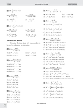
![23. X s
s
( )
( )
=
+ +
1
2 1 42
(A) e t u tt-0 5.
sin ( ) (B)
1
2
e t u tt-
sin ( )
(C)
1
4
0 5
e t u tt- .
sin ( ) (D) e t u tt-
sin ( )
24. X s e
d
ds s
s
( )
( )
=
+
æ
è
çç
ö
ø
÷÷
-2
2
1
1
(A) - --
te u tt
( )1 (B) - --
te u tt
( )1
(C) - - -- -
( ) ( )( )
t e u tt
2 22 2
(D) te u tt-
-( )1
Statement for Q.25–29:
Given the transform pair below. Determine the
time signal y t( ) and choose correct option.
cos ( ) ( )2t u t X sL
¬ ®¾ .
25. Y s s X s( ) ( ) ( )= + 1
(A) [cos sin ] ( )2 2 2t t u t- (B) cos
sin
( )2
2
2
t
t
u t+
æ
è
ç
ö
ø
÷
(C) [cos sin ] ( )2 2 2t t u t+ (D) cos
sin
( )2
2
2
t
t
u t-
æ
è
ç
ö
ø
÷
26. Y s X s( ) ( )= 3
(A) cos ( )
2
3
t u t
æ
è
ç
ö
ø
÷ (B)
1
3
2
3
cos ( )t u t
æ
è
ç
ö
ø
÷
(C) cos ( )6t u t (D)
1
3
6cos ( )t u t
27. Y s X s( ) ( )= + 2
(A) cos ( ) ( )2 2t u t- (B) e t u tt2
2cos ( )
(C) cos ( ) ( )2 2t u t+ (D) e t u tt-2
2cos ( )
28. Y s
X s
s
( )
( )
= 2
(A) 4 2cos ( )t u t (B)
1 2
4
- cos
( )
t
u t
(C) t t u t2
2cos ( ) (D)
cos
( )
2
2
t
t
u t
29. Y s
d
ds
e X ss
( ) [ ( )]= -3
(A) t t u tcos ( ) ( )2 3 3- - (B) t t u tcos ( ) ( )2 3-
(C) - - -t t u tcos ( ) ( )2 3 3 (D) - -t t u tcos ( ) ( )2 3
Statement for Q.30–33:
Given the transform pair
x t u t
s
s
L
( ) ( ) ¬ ®¾
+
2
22
.
Determine the Laplace transform Y s( ) of the given
time signal in question and choose correct option.
30. y t x t( ) ( )= - 2
(A)
2
2
2
2
se
s
s-
+
(B)
2
2
2
2
se
s
s
+
(C)
2 2
2 12
( )
( )
s
s
-
- +
(D)
2 2
2 12
( )
( )
s
s
+
+ +
31. y t x t
dx t
dt
( ) ( ) *
( )
=
(A)
4
2
3
2 2
s
s( )+
(B)
4
22 2
( )s +
(C)
-
+
4
2
3
2 2
s
s( )
(D)
4
22 2
( )s +
32. y t e x tt
( ) ( )= -
(A)
2 1
1 22
( )
( )
s
s
+
+ +
(B)
2 1
2 22
( )s
s s
+
+ +
(C)
2 1
2 42
( )s
s s
+
+ +
(D)
2 1
22
( )s
s s
+
+
33. y t tx t( ) ( )= 2
(A)
8 4
2
2
2 2
-
+
s
s( )
(B)
4 8
2
2
2 2
s
s
-
+( )
(C)
4
1
2
2
s
s +
(D)
s
s
2
2
1+
Statement for Q.34–43:
Determine the bilateral laplace transform and
choose correct option.
34. x t e u tt
( ) ( )= +-
2
(A)
e
s
s2 1
1
( )+
+
, Re ( )s > -1
(B)
1
1 + s
, Re ( )s < - 1
(C)
e
s
s2 1
1
( )+
+
, Re ( )s < - 1
(D)
1
1 + s
, Re ( )s > -1
Chap 5.3The Laplace Transform
Page
271
GATE EC BY RK Kanodia
www.gatehelp.com](https://image.slidesharecdn.com/a-150815031147-lva1-app6892/85/A-gate-by-rk-kanodia-177-320.jpg)
![35. x t u t( ) ( )= - + 3
(A)
1 3
- -
e
s
s
, Re ( )s > 0
(B)
- -
e
s
s3
, Re ( )s < 0
(C)
1 3
- -
e
s
s
, Re ( )s < 0
(D)
- -
e
s
s3
, Re ( )s > 0
36. y t t( ) ( )= +d 1
(A) es
, Re( )s > 0 (B) es
, Re ( )s < 0
(C) es
, all s (D) None of above
37. x t t u t( ) sin ( )=
(A)
1
1 2
( )+ s
, Re ( )s < 0
(B)
1
1 2
( )+ s
, Re ( )s > 0
(C)
-
+
1
1 2
( )s
, Re ( )s < 0
(D)
-
+
1
1 2
( )s
, Re ( )s > 0
38. x t e u t e u t e u t
t
t t
( ) ( ) ( ) ( )= + + -
-
-2
(A)
6 2 2
2 1 1
2
2
s s
s s
+ -
+ -( )( )
, Re ( ) .s < - 0 5
(B)
6 2 2
2 1 1
2
2
s s
s s
+ -
+ -( )( )
, - >1 Re ( )s > 1
(C)
1
0 5
1
1
1
1s s s+
+
+
+
-.
, -1 < Re ( )s < 1
(D)
1
0 5
1
1
1
1s s s+
+
+
-
-.
, - <0 5. Re ( )s < 1
39. x t e t u t e u t e u tt t
t
( ) cos ( ) ( ) ( )= - + +-
2 2
(A)
( )
( ) .
1
1 4
1
1
1
0 52
-
- +
+
+
+
-
s
s s s
, 0 5. < Re ( )s < 1
(B)
( )
( ) .
1
1 4
1
1
1
0 52
-
- +
+
+
+
-
s
s s s
, - <1 Re ( )s < 1
(C)
( )
( ) .
s
s s s
-
- +
+
+
+
-
1
1 4
1
1
1
0 52
, 0 5. < Re ( )s < 1
(D)
( )
( ) .
s
s s s
-
- +
+
+
+
-
1
1 4
1
1
1
0 52
, - <1 Re ( )s < 1
40. x t e u tt
( ) ( )( )
= ++3 6
3
(A)
e
s
s3
3-
, Re ( )s > 3
(B)
e
s
s3
3-
, Re ( )s < 3
(C)
e
s
s3 1
3
( )-
-
, Re ( )s > 3
(D)
e
s
s3 1
3
( )-
-
, Re ( )s < 3
41. x t t u t e u tt
( ) cos ( ) * ( )= - -
3
(A)
-
+ +
s
s s( )( )1 92
, Re ( )s > 0
(B)
-
+ +
s
s s( )( )1 92
, - <1 Re ( )s < 0
(C)
s
s s( )( )+ +1 92
, - <1 Re ( )s < 0
(D)
s
s s( )( )+ +1 92
, Re ( )s > 0
42. x t e t u tt
( ) sin ( ) ( )= + +2 4 2
(A)
e
s
s2 1
2
1 4
( )
( )
-
- +
, Re ( )s > 1
(B)
e
s
s2 1
2
1 4
( )
( )
-
- +
, Re ( )s < 1
(C)
e
s
s( )
( )
-
- +
2
2
1 4
, Re ( )s > 1
(D)
e
s
s( )
( )
-
- +
2
2
1 4
, Re ( )s < 1
43. x t e
d
dt
e u tt t
( ) [ ( )]= --2
(A)
1
1
-
+
s
s
, Re ( )s < - 1
(B)
1
1
-
+
s
s
, Re ( )s > -1
(C)
s
s
-
+
1
1
, Re ( )s < - 1
(D)
s
s
-
+
1
1
, Re ( )s > -1
Statement for Q.44–49:
Determine the corresponding time signal for given
bilateral Laplace transform.
44. X s
e
s
s
( ) =
+
5
2
with ROC: Re ( )s < -2
(A) e u tt- +
+2 5
5( )
( )
Page
272
UNIT 5 Signal & SystemGATE EC BY RK Kanodia
www.gatehelp.com](https://image.slidesharecdn.com/a-150815031147-lva1-app6892/85/A-gate-by-rk-kanodia-178-320.jpg)
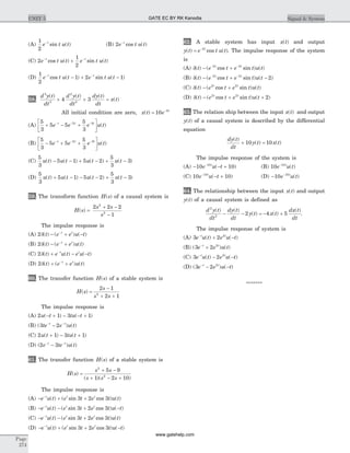
![SOLUTIONS
1. (B) X s x t e dtst
( ) ( )= -
¥
ò0
= =-
¥ -
òe dt
e
s
st
s
2
2
2. (A) X s x t e dtt
( ) ( )= -
¥
ò
3
0
= + -
¥
òu t dtt
( )2 3
0
= =-
¥
òe dt
s
t3
0
1
3. (A) X s e e dt
s
t st
( ) = =
+
- -
¥
ò
2
0
1
2
4. (C) X s x t e dtst
( ) ( )= -
¥
ò0
= - + -
¥
òe u t e dtt st2
0
2( )
= =
-
-
-
-
òe dt
e
s
t s
s
( )
( )
2
0
2 2 2
1
2
=
-
-
- -
1
2
2 2
e
s
s( )
5. (C) X s
e e
j
e dt
s
j t j t
st
( )
( )
=
-
=
+
-
-
¥
ò
5 5
0
2
2
5
25
6. (B) X s e dtst
( ) = -
ò0
2
=
- -
1 2
e
s
s
7. (B) p t te u t P s
s
t L
( ) ( ) ( )
( )
= ¬ ®¾ =
+
- 1
1 2
x t
d
dt
p t X s
s
s
L
( ) ( ) ( )
( )
= ¬ ®¾ =
+ 1 2
8. (A) p t tu t P s
s
L
( ) ( ) ( )= ¬ ®¾ =
1
2
q t t u t Q s
s
s
L
( ) cos ( ) ( )= ¬ ®¾ =
+
2
42 2
p
p
x t p t q t X s P s Q sL
( ) ( ) * ( ) ( ) ( ) ( )= ¬ ®¾ =
Þ =
+
X s
s s
( )
( )
1
42 2
p
9. (C) p t tu t P s
s
L
( ) ( ) ( )= ¬ ®¾ =
1
2
q t tp t Q s
d
ds
P s
s
L
( ) ( ) ( ) ( )= - ¬ ®¾ = =
-2
3
x t tq t X s
d
ds
Q s
s
L
( ) ( ) ( ) ( )= - ¬ ®¾ = =
6
4
t u t
n
s
n L
n
( )
!
¬ ®¾ +1
10. (D) p t u t P s
s
L
( ) ( ) ( )= ¬ ®¾ =
1
q t u t Q s
e
s
L
s
( ) ( ) ( )= - ¬ ®¾ =
-
1 2
r t e u t R s
s
t L
( ) ( ) ( )= ¬ ®¾ =
+
-2 1
2
v t e u t V s
e
s
t L
s
( ) ( ) ( )
( )
= - ¬ ®¾ =-
- +
2
2
2
1
x t q t v t X s Q s V sL
( ) ( ) * ( ) ( ) ( ) ( )= ¬ ®¾ =
Þ =
+
- +
X s
e
s
s
( )
( )2 1
2
11. (B) p t e t u t P s
s
s
t L
( ) cos ( ) ( )
( )
= ¬ ®¾ =
+
+ +
-3
2
2
3
3 4
p d
s
p d
P s
s
t
L
( ) ( )
( )
t t t t
-¥ -¥
ò ò¬ ®¾ +
1
0
Þ =
+
+ +
X s
s
s s
( )
( )
[( ) ]
3
3 42
12. (A) p t e t u t P s
s
s
t L
( ) cos ( ) ( )
( )
= ¬ ®¾ =
+
+ +
- 1
1 12
q t
d
dt
p t Q s
s s
s
L
( ) ( ) ( )
( )
( )
= ¬ ®¾ =
+
+ +
1
1 12
x t tq t X s
d
ds
Q sL
( ) ( ) ( ) ( )= ¬ ®¾ = -
Þ =
- + +
+ +
X s
s s
s s
( )
( )
( )
2
2 2
4 2
2 2
13. (B) X s
s
s s
A
s
B
s
( )
( )
=
+
+ +
=
+
+
+
3
3 2 1 22
A
s
s s
=
+
+
=
=-
3
2
2
1
, B
s
s s
=
+
+
= -
=-
3
1
1
2
x t e e u tt t
( ) [ ] ( )= -- -
2 2
14. (A) X s
s s s s
( )
( ) ( ) ( ) ( )
= -
+ +
= -
+
+
+
2
1
2 3
2
1
2
1
3
x t t e e u tt t
( ) ( ) ( ) ( )= + -- -
2 3 3
d
15. (C) X s
s
s s
A
s
B
s
( )
( ) ( )
=
-
+ +
=
+
+
+
2 1
2 1 1 12 2
B s s
= - = -=-
( )2 2 31
, A = 2
x t( ) = x t e te u tt t
( ) [ ] ( )= -- -
2 3
16. (B) X s
s
s s s
A
s
B
s
C
s
( ) =
+
+ +
= +
+
+
+
5 4
3 2 1 23 2
A sX s s
= ==
( ) 0
2, B s X s s
= + ==-
( ) ( )1 11
,
C s X s s
= + = -=-
( ) ( )2 32
x t e e u tt t
( ) [ ] ( )= + -- -
2 3 2
17. (C) X s
s
s s s
( )
( )( )
=
-
+ + +
2
2
3
2 2 1
=
+
+
+
+
+
A
s
B
s
C
s( ) ( ) ( )2 1 1 2
Chap 5.3The Laplace Transform
Page
275
GATE EC BY RK Kanodia
www.gatehelp.com](https://image.slidesharecdn.com/a-150815031147-lva1-app6892/85/A-gate-by-rk-kanodia-180-320.jpg)
![A s X s s
= + ==-
( ) ( )2 12
, C s X s
s
= + = -
=-
( ) ( )1 22
1
A B+ = 1 Þ B = 0
x t e te u tt t
( ) [ ] ( )= -- -2
18. (A) X s
s
s s
( ) =
+
+ +
3 2
2 102
=
+
+ +
-
+ +
3 1
1 3
1
1 32 2 2 2
( )
( ) ( )
s
s s
x t e t e t u tt t
( ) cos sin ( )= -
é
ëê
ù
ûú
- -
3 3
1
3
3
19. (C) X s
s s
s s s
( )
( )( )
=
+ +
+ + +
4 8 10
2 2 5
2
2
=
+
+
+
+ +
+
+ +
A
s
B s
s
C
s( )
( )
( ) ( )2
1
1 2 1 22 2 2 2
A s X s s
= + ==-
( ) ( )2 22
A B B+ = Þ =4 2
5 2 2 10A B C+ + = Þ C = -2
x t e e t e t u tt t t
( ) [ cos sin ] ( )= + -- - -
2 2 2 22
20. (B) X s
s s
s s s
( )
( )( )
=
+ +
+ + +
3 10 10
2 6 10
2
2
=
+
+
+
+ +
+
+ +
A
s
B s
s
C
s( )
( )
( ) ( )2
3
3 1 3 12 2
A s X s s
= + ==-
( ) ( )2 12
, A B B+ = Þ =3 2
10 6 2 10A B C+ + = Þ C = -6
x t e e t e t u tt t t
( ) [ cos sin ] ( )= + -- - -2 3 3
2 6
21. (D) X s
s s e
s s
s
( )
( )
=
+ + +
+ +
-
2 11 16
5 6
2 2
2
= +
+
+
+
+
+
-
+
- -
2
2 3 2 3
2 2
A
s
B
s
e
s
e
s
s s
( ) ( ) ( ) ( )
A
s s s
s s s
=
+ + +
+ +
=
=-
( )( )
( )
2 2 11 16
5 6
2
2
2
2
B
s s s
s s s
=
+ + +
+ +
= -
=-
( )( )
( )
3 2 11 16
5 6
1
2
2
3
x t t e e u t e e u tt t t t
( ) ( ) [ ] ( ) [ ] (( ) ( )
= + - + -- - - - - -
2 2 2 3 2 2 3 2
d - 2)
22. (C) P s
s
p t t u tL
( ) ( ) sin ( )=
+
¬ ®¾ =
1
9
1
3
32
Q s
d
ds
P s q tL
( ) ( ) ( )= ¬ ®¾
2
2
= - =( ) ( ) sin ( )1
3
32 2
2
t p t
t
t u t
R s sQ s r t
d
dt
q t qL
( ) ( ) ( ) ( ) ( )= ¬ ®¾ = - -
0
= +
2
3
3 32t
t u t t t u tsin ( ) cos ( )
V s
s
v t e u tL t
( ) ( ) ( )=
+
¬ ®¾ = -1
3
3
x t v t r t( ) ( ) ( )= + = + +
é
ëê
ù
ûú
-2
3
3 32 3t
t u t t t u t e u tt
sin ( ) cos ( ) ( )
23. (C) P
s
a
ap atLæ
è
ç
ö
ø
÷ ¬ ®¾ ( )
1
1 4
1
2
22
( )
sin ( )
s
e t u tL t
+ +
¬ ®¾ -
x t e t u tL t
( ) sin ( ).
¬ ®¾ -1
4
0 5
24. (C) P s
s
p t te u tL t
( )
( )
( ) ( )=
+
¬ ®¾ = -1
1 2
Q s
d
ds
P s q t tp t t e u tL t
( ) ( ) ( ) ( ) ( )= ¬ ®¾ = - = - -2
X s e Q s x t q ts L
( ) ( ) ( ) ( )= ¬ ®¾ = --2
2
Þ = - - --
x t t e u tt
( ) ( ) ( )( )
2 22
25. (A) sX s X s
dx t
dt
x tL
( ) ( )
( )
( )+ ¬ ®¾ +
Þ = - +y t t t u t( ) ( sin cos ) ( )2 2 2
26. (B) X
s
a
ax atLæ
è
ç
ö
ø
÷ ¬ ®¾ ( )
X s t u tL
( ) cos ( )3
1
3
2
3
¬ ®¾
æ
è
ç
ö
ø
÷
27. (D) X s e x tL t
( ) ( )+ ¬ ®¾ -
2 2
28. (B) P s
X s
s
x dL
t
( )
( )
( )= ¬ ®¾
-¥
ò t t
L
t
u d
t
¬ ®¾ =
-¥
òcos ( )
sin
2
2
2
t t t
P s
s
d
t
u tL
t
( ) sin cos
( )¬ ®¾ =
-
ò
2
2
1 2
40
t
t ,
29. (C) P s e X s p t x ts L
( ) ( ) ( ) ( )= ¬ ®¾ = --3
3
= - -cos ( ) ( )2 3 3t u t
Q s
d
ds
P s q t p tL
( ) ( ) ( ) ( )= ¬ ®¾ = -
= - - -t t u tcos ( ) ( )2 3 3 .
30. (A) x t e X sL s
( ) ( )- ¬ ®¾ -
2 2
, Y s
se
s
s
( ) =
+
-
2
2
2
2
31. (A) p t
d
dt
x t P s sX sL
( ) ( ) ( ) ( )= ¬ ®¾ =
y t x t p t Y s P s X s s X sL
( ) ( ) * ( ) ( ) ( ) ( ) ( ( ))= ¬ ®¾ = = 2
32. (A) e x t X s
s
s
t L-
¬ ®¾ + =
+
+ +
( ) ( )
( )
( )
1
2 1
1 22
Page
276
UNIT 5 Signal & SystemGATE EC BY RK Kanodia
www.gatehelp.com](https://image.slidesharecdn.com/a-150815031147-lva1-app6892/85/A-gate-by-rk-kanodia-181-320.jpg)
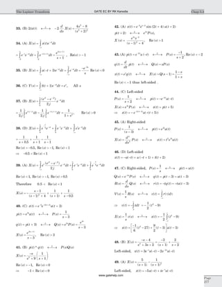
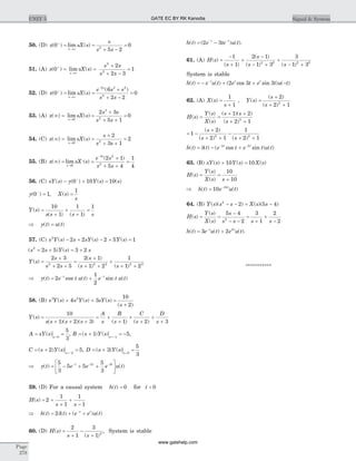
![Statement forQ.1-12:
Determine the z-transform and choose correct
option.
1. x n n k k[ ] [ ],= - >d 0
(A) z zk
, > 0 (B) z zk-
>, 0
(C) z zk
, ¹ 0 (D) z zk-
¹, 0
2. x n n k k[ ] [ ],= + >d 0
(A) z zk-
¹, 0 (B) z zk
, ¹ 0
(C) z k-
, all z (D) zk
, all z
3. x n u n[ ] [ ]=
(A)
1
1
11
-
>-
z
z, | | (B)
1
1
11
-
<-
z
z, | |
(C)
z
z
z
1
11
-
<-
, | | (D)
z
z
z
1
11
-
>-
, | |
4. x n u n u n
n
[ ] ( [ ] [ ])=
æ
è
ç
ö
ø
÷ - -
1
4
5
(A)
z
z z
z
5 5
4
0 25
0 25
0 25
-
-
>
.
( . )
, . (B)
z
z z
z
5 5
4
0 25
0 25
0
-
-
>
.
( . )
,
(C)
z
z z
z
5 5
3
0 25
0 25
0 25
-
-
<
.
( . )
, . (D)
z
z z
5 5
4
0 25
0 25
-
-
.
( . )
, all z
5. x n u n[ ] [ ]=
æ
è
ç
ö
ø
÷ -
1
4
4
(A)
4
4 1
1
4
z
z
z
-
>, | | (B)
4
4 1
1
4
z
z
z
-
<, | |
(C)
1
1 4
1
4-
>
z
z, | | (D)
1
1 4
1
4-
<
z
z, | |
6. x n u nn
[ ] [ ]= - -3 1
(A)
z
z
z
3
3
-
>, | | (B)
z
z
z
3
3
-
<, | |
(C)
3
3
3
-
>
z
z, | | (D)
3
3
3
-
<
z
z, | |
7. x n
n
[ ]
| |
=
æ
è
ç
ö
ø
÷
2
3
(A)
-
- -
- < < -
5
2 3 3 2
3
2
2
3
z
z z
z
( )( )
,
(B)
-
- -
< <
5
2 3 3 2
2
3
3
2
z
z z
z
( )( )
, | |
(C)
5
2 3 3 2
2
3
2
3
z
z z
z
( ) ( )
, | |
- -
< <
(D)
5
2 3 3 2
3
2
2
3
z
z z
z
( )( )
,
- -
- < < -
8. x n u n u n
n n
[ ] [ ] [ ]=
æ
è
ç
ö
ø
÷ +
æ
è
ç
ö
ø
÷ - -
1
2
1
4
1
(A)
1
1
1
2
1
1
1
4
1
4
1
21 1
-
-
-
< <
- -
z z
z, | |
(B)
1
1
1
2
1
1
1
4
1
4
1
21 1
-
+
-
< <
- -
z z
z, | |
(C)
1
1
1
2
1
1
1
4
1
21 1
-
-
-
>
- -
z z
z, | |
(D) None of the above
CHAPTER
5.4
THE Z-TRANSFORM
Page
279
GATE EC BY RK Kanodia
www.gatehelp.com](https://image.slidesharecdn.com/a-150815031147-lva1-app6892/85/A-gate-by-rk-kanodia-184-320.jpg)
![33. X z
z
z( ) , | |=
-
<-
1
1 4
1
42
(A) - - - ++
=
¥
å2 2 12 1
0
( )
[ ( )]k
k
n kd
(B) - - + ++
=
¥
å2 2 12 1
0
( )
[ ( )]k
k
n kd
(C) - + ++
=
¥
å2 2 12 1
0
( )
[ ( )]k
k
n kd
(D) - - ++
=
¥
å2 2 12 1
0
( )
[ ( )]k
k
n kd
34. X z z z( ) ln ( ) , | |= + >-
1 01
(A)
( )
[ ]
-
-
-
1
1
1k
k
nd (B)
( )
[ ]
-
+
-
1
1
1k
k
nd
(C)
( )
[ ]
-
-
1
1
k
k
nd (D)
( )
[ ]
-
+
1
1
k
k
nd
35. If z-transform is given by
X z z z( ) cos ( ), | |= >-3
0,
The value of x[ ]12 is
(A) -
1
24
(B)
1
24
(C) -
1
6
(D)
1
6
36. X z( ) of a system is specified by a pole zero pattern
in fig. P.5.4.36.
Consider three different solution of x n[ ]
x n u nn
n
1 2
1
3
[ ] [ ]= -
æ
è
ç
ö
ø
÷
é
ë
ê
ê
ù
û
ú
ú
x n u n u nn
n2 2 1
1
3
[ ] [ ] [ ]= - - -
x n u n u nn
n3 2 1
1
3
1[ ] [ ] [ ]= - - + - -
Correct solution is
(A) x n1[ ] (B) x n2[ ]
(C) x n3[ ] (D) All three
37. Consider three different signal
x n u nn
n
1 2
1
2
[ ] [ ]= -
æ
è
ç
ö
ø
÷
é
ë
ê
ê
ù
û
ú
ú
x n u n u nn
n2 2 1
1
2
1[ ] [ ] [ ]= - - - + - -
x n u n u nn
n3 2 1
1
2
[ ] [ ] [ ]= - - - -
Fig. P.5.4.37 shows the three different region.
Choose the correct option for the ROC of signal
R1 R2 R3
(A) x n1[ ] x n2[ ] x n3[ ]
(B) x n2[ ] x n3[ ] x n1[ ]
(C) x n1[ ] x n3[ ] x n2[ ]
(D) x n3[ ] x n2[ ] x n1[ ]
38. Given
X z
z
z z
( ) =
+
-
æ
è
ç
ö
ø
÷ +
æ
è
ç
ö
ø
÷
-
- -
1
7
6
1
1
2
1
1
3
1
1 1
For three different ROC consider there different
solution of signal x n[ ] :
(a) | |z >
1
2
, x n u nn
n
[ ] [ ]= -
-æ
è
ç
ö
ø
÷
é
ë
ê
ê
ù
û
ú
ú
-
1
2
1
31
(b) | |z <
1
3
, x n u nn
n
[ ] [ ]=
-
+
-æ
è
ç
ö
ø
÷
é
ë
ê
ê
ù
û
ú
ú
- +-
1
2
1
3
11
(c)
1
3
1
2
< <| |z , x n u n u nn
n
[ ] [ ] [ ]= - - - -
-æ
è
ç
ö
ø
÷-
1
2
1
1
31
Correct solutions are
(A) (a) and (b) (B) (a) and (c)
(C) (b) and (c) (D) (a), (b), (c)
Page
282
UNIT 5 Signal & System
Re
2
Im
z - plane
1
3
Fig. P.5.4.36
R2
R1
R3
2
Re
Im
z - plane
1
2
Fig. P5.4.37
GATE EC BY RK Kanodia
www.gatehelp.com](https://image.slidesharecdn.com/a-150815031147-lva1-app6892/85/A-gate-by-rk-kanodia-185-320.jpg)
![39. X z( ) has poles at z = 1 2 and z = -1. If x [ ]1 1=
x [ ]- =1 1, and the ROC includes the point z = 3 4. The
time signal x n[ ] is
(A)
1
2
1 11n
n
u n u n-
- - - -[ ] ( ) [ ]
(B)
1
2
1 1n
n
u n u n[ ] ( ) [ ]- - - -
(C)
1
2
11n
u n u n-
+ - +[ ] [ ]
(D)
1
2
1n
u n u n[ ] [ ]+ - +
40. x n[ ] is right-sided, X z( ) has a signal pole, and
x[ ]0 2= , x[ ]2 1 2= . x n[ ] is
(A)
u n
n
[ ]-
-
2 1
(B)
u n
n
[ ]
2 1-
(C)
u n
n
[ ]-
+
2 1
(D)
u n
n
[ ]-
+
2 1
41. The z-transform function of a stable system is given
as
H z
z
z z
( )
( ) ( )
=
-
- +
-
- -
2
3
2
1 2 1
1
2
1
1 1
The impuse response h n[ ] is
(A) 2 1
1
2
n
n
u n u n[ ] [ ]- + -
æ
è
ç
ö
ø
÷
(B) 2 1
1
2
n
n
u n u n[ ] [ ]- - +
-æ
è
ç
ö
ø
÷
(C) - - - +
-æ
è
ç
ö
ø
÷2 1
1
2
n
n
u n u n[ ] [ ]
(D) 2
1
2
n
n
u n u n[ ] [ ]-
æ
è
ç
ö
ø
÷
42. Let x n n n[ ] [ ] [ ]= - + +d d2 2 . The unilateral
z-transform is
(A) z-2
(B) z2
(C) - -
2 2
z (D) 2 2
z
43. The unilateral z-transform of signal x n u n[ ] [ ]= + 4
is
(A) 1 32 4
+ + + +z z z z (B)
1
1 - z
(C) 1 1 2 3 4
+ + + +- - - -
z z z z (D)
1
1 1
- -
z
44. The transfer function of a causal system is given as
H z
z
z z
( ) =
- -
5
6
2
2
The impulse response is
(A) ( ( ) ) [ ]3 1 2 1n n n
u n+ - +
(B) ( ( ) ) [ ]3 2 21n n
u n+
+ -
(C) ( ( ) ) [ ]3 1 21 1n n n
u n- +
+ -
(D) ( ( ) ) [ ]3 21 1n n
u n- +
- -
45. A causal system has input
x n n n n[ ] [ ] [ ] [ ]= + - - -d d d
1
4
1
1
8
2 and output
y n n n[ ] [ ] [ ]= - -d d
3
4
1 .
The impulse response of this system is
(A)
1
3
5
1
2
2
1
4
-æ
è
ç
ö
ø
÷ -
æ
è
ç
ö
ø
÷
é
ë
ê
ê
ù
û
ú
ú
n n
u n[ ]
(B)
1
3
5
1
2
2
1
4
æ
è
ç
ö
ø
÷ +
-æ
è
ç
ö
ø
÷
é
ë
ê
ê
ù
û
ú
ú
n n
u n[ ]
(C)
1
3
5
1
2
2
1
4
æ
è
ç
ö
ø
÷ -
-æ
è
ç
ö
ø
÷
é
ë
ê
ê
ù
û
ú
ú
n n
u n[ ]
(D)
1
3
5
1
2
2
1
4
æ
è
ç
ö
ø
÷ +
æ
è
ç
ö
ø
÷
é
ë
ê
ê
ù
û
ú
ú
n n
u n[ ]
46. A causal system has input x n u nn
[ ] ( ) [ ]= -3 and
output
y n u nn
n
[ ] ( ) [ ]= -
æ
è
ç
ö
ø
÷
é
ë
ê
ê
ù
û
ú
ú
4 2
1
2
.
The impulse response of this system is
(A) 7
1
2
10
1
2
æ
è
ç
ö
ø
÷ -
æ
è
ç
ö
ø
÷
é
ë
ê
ê
ù
û
ú
ú
n n
u n[ ] (B) 7 2 10
1
2
( ) [ ]n
n
u n-
æ
è
ç
ö
ø
÷
é
ë
ê
ê
ù
û
ú
ú
(C) 10
1
2
7 2
2
æ
è
ç
ö
ø
÷ -
é
ë
ê
ê
ù
û
ú
ú
( ) [ ]n
u n (D) 10 2 7
1
2
( ) [ ]n
n
u n-
æ
è
ç
ö
ø
÷
é
ë
ê
ê
ù
û
ú
ú
47. A system has impulse response
h n u nn
[ ] [ ]=
1
2
The output y n[ ] to the input x n[ ] is given by
y n n[ ] [ ]= -2 4d . The input x n[ ] is
(A) 2 4 5d d[ ] [ ]- - - - -n n (B) 2 4 5d d[ ] [ ]n n+ - +
(C) 2 4 5d d[ ] [ ]- + - - +n n (D) 2 4 5d d[ ] [ ]n n- - -
Chap 5.4The z-Transform
Page
283
GATE EC BY RK Kanodia
www.gatehelp.com](https://image.slidesharecdn.com/a-150815031147-lva1-app6892/85/A-gate-by-rk-kanodia-186-320.jpg)
![48. A system is described by the difference equation
y n y n x n[ ] [ ] [ ]- - = -
1
2
1 2 1
The impulse response of the system is
(A)
-
--
1
2
12n
u n[ ] (B)
1
2
12n
u n-
+[ ]
(C)
1
2
22n
u n-
-[ ] (D)
-
--
1
2
22n
u n[ ]
49. A system is described by the difference equation
y n x n x n x n x n[ ] [ ] [ ] [ ] [ ]= - - + - - -2 4 6
The impulse response of system is
(A) d d d d[ ] [ ] [ ] [ ]n n n n- + + + - +2 2 4 4 6 6
(B) d d d d[ ] [ ] [ ] [ ]n n n n+ - - - + -2 2 4 4 6 6
(C) d d d d[ ] [ ] [ ] [ ]n n n n- - + - - -2 4 6
(D) d d d d[ ] [ ] [ ] [ ]n n n n- + + + - +2 4 6
50. The impulse response of a system is given by
h n u nn
[ ] [ ]= -
3
4
1 .
The difference equation representation for this
system is
(A) 4 1 3 1y n y n x n[ ] [ ] [ ]- - = -
(B) 4 1 3 1y n y n x n[ ] [ ] [ ]- + = +
(C) 4 1 3 1y n y n x n[ ] [ ] [ ]+ - = - -
(D) 4 1 3 1y n y n x n[ ] [ ] [ ]+ + = +
51. The impulse response of a system is given by
h n n n[ ] [ ] [ ]= - -d d 5
The difference equation representation for this
system is
(A) y n x n x n[ ] [ ] [ ]= - - 5 (B) y n x n x n[ ] [ ] [ ]= - + 5
(C) y n x n x n[ ] [ ] [ ]= + -5 5 (D) y n x n x n[ ] [ ] [ ]= - +5 5
52. The transfer function of a system is given by
H z
z z
z z
( )
( )
=
-
- -
3 2
1
4
2
The system is
(A) Causal and Stable
(B) Causal, Stable and minimum phase
(C) Minimum phase
(D) None of the above
53. The z-transform of a signal x n[ ] is given by
X z
z z
( ) =
- +- -
3
1
10
3
1 2
If X z( ) converges on the unit circle, x n[ ] is
(A) - - - --
+
1
3 8
3
8
11
3
n
n
u n u n[ ] [ ]
(B)
1
3 8
3
8
11
3
n
n
u n u n-
+
- - -[ ] [ ]
(C)
1
3 8
3
81
3
n
n
u n u n-
+
- -[ ] [ ]
(D) - - --
+
1
3 8
3
81
3
n
n
u n u n[ ] [ ]
54. The transfer function of a system is given as
H z
z
z
z( ) , | |=
-
æ
è
ç
ö
ø
÷
>
-
-
4
1
1
4
1
4
1
1
2
The h n[ ] is
(A) Stable (B) Causal
(C) Stable and Causal (D) None of the above
55. The transfer function of a system is given as
H z
z
z z
( ) =
+
æ
è
ç
ö
ø
÷
-
æ
è
ç
ö
ø
÷ -
æ
è
ç
ö
ø
÷
2
1
2
1
2
1
3
.
Consider the two statements
Statement(i) : System is causal and stable.
Statement(ii) : Inverse system is causal and stable.
The correct option is
(A) (i) is true
(B) (ii) is true
(C) Both (i) and (ii) are true
(D) Both are false
56. The impulse response of a system is given by
h n u n u n
n n
[ ] [ ] [ ]=
-æ
è
ç
ö
ø
÷ -
-æ
è
ç
ö
ø
÷10
1
2
9
1
4
For this system two statement are
Statement (i): System is causal and stable
Statement (ii): Inverse system is causal and stable.
Page
284
UNIT 5 Signal & SystemGATE EC BY RK Kanodia
www.gatehelp.com](https://image.slidesharecdn.com/a-150815031147-lva1-app6892/85/A-gate-by-rk-kanodia-187-320.jpg)
![The correct option is
(A) (i) is true (B) (ii) is true
(C) Both are true (D) Both are false
57. The system
y n cy n y n x n x n[ ] [ ] . [ ] [ ] [ ]= - - - + - + -1 0 12 2 1 2
is stable if
(A) c < 112. (B) c > 112.
(C) | | .c < 112 (D) | | .c > 112
58. Consider the following three systems
y n y n x n x n x n1 0 2 1 0 3 1 0 02 2[ ] . [ ] [ ] . [ ] . [ ]= - + - - + -
y n x n x n2 0 1 1[ ] [ ] . [ ]= - -
y n y n x n x n3 0 5 1 0 4 0 3 1[ ] . [ ] . [ ] . [ ]= - + - -
The equivalent system are
(A) y n1[ ] and y n2[ ] (B) y n2[ ] and y n3[ ]
(C) y n3[ ] and y n1[ ] (D) all
59. The z-transform of a causal system is given as
X z
z
z z
( )
.
. .
=
-
- +
-
- -
2 15
1 15 0 5
1
1 2
The x[ ]0 is
(A) -15. (B) 2
(C) 1.5 (D) 0
60. The z-transform of a anti causal system is
X z
z
z z
( ) =
-
- +
12 21
3 7 12 2
The value of x[ ]0 is
(A) -
7
4
(B) 0
(C) 4 (D) Does not exist
61. Given the z-transforms
X z
z z
z z
( )
( )
=
-
- +
8 7
4 7 32
The limit of x[ ]¥ is
(A) 1 (B) 2
(C) ¥ (D) 0
62. The impulse response of the system shown in fig.
P5.4.62 is
(A) 2 1 1
1
2
2
2
n
n
u n n
-
æ
è
çç
ö
ø
÷÷
+ - +( ( ) ) [ ] [ ]d
(B)
2
2
1 1
1
2
n
n
u n n( ( ) ) [ ] [ ]+ - + d
(C) 2 1 1
1
2
2
2
n
n
u n n
-
æ
è
çç
ö
ø
÷÷
+ - -( ( ) ) [ ] [ ]d
(D)
2
2
1 1
1
2
n
n
u n n[ ( ) ] [ ] [ ]+ - - d
63. The system diagram for the transfer function
H z
z
z z
( ) =
+ +2
1
is shown in fig. P5.4.63. This system diagram is a
(A) Correct solution
(B) Not correct solution
(C) Correct and unique solution
(D) Correct but not unique solution
*****************
Chap 5.4The z-Transform
Page
285
X z( ) Y z( )
z-1
z-1
+ z-1
Fig. P5.4.62
X z( ) Y z( )
z-1
z-1
+
+
+
Fig. P5.4.63
GATE EC BY RK Kanodia
www.gatehelp.com](https://image.slidesharecdn.com/a-150815031147-lva1-app6892/85/A-gate-by-rk-kanodia-188-320.jpg)
![24. (A) X z
z z
z z
z
z z
( ) =
-
+
=
-
+ --
-
- -
2
2 1
1
1 2
3
3
2
1 3
1
3
2
=
+
-
-
-
-
2
1 2
1
1
1
2
1
1z z
, ROC :
1
2
2< <| |z
Þ = - - - -x n u n u nn
n
[ ] ( ) [ ] [ ]2 2 1
1
2
25. (A) x n[ ] is right sided
X z
z z
z z z
( ) =
-
-
=
+
+
-
-
- - -
1
4
1 16
49
32
1 4
47
32
1 4
1
1 1 1
Þ = - +
é
ëê
ù
ûúx n u nn n
[ ] ( ) [ ]
49
32
4
47
32
4
26. (C) x n[ ] is right sided
X z
z z
z( ) = +
+
+
-
-
æ
è
ç
ö
ø
÷- -
2
1
1
1
11 1
2
Þ = + + - - +x n n u nn
[ ] [ ] (( ) ) [ ]2 2 1 1 2d
27. (A) d d d[ ] [ ] [ ]n n n+ - + -2 6 4 8
28. (B) x n[ ] is right sided, x n
k
n k
k
[ ] [ ]= -
=
å
1
5
10
d
29. (D) x n[ ] is right sided signal
X z z z z( ) = + + +- - -
1 3 31 2 3
Þ = + - + - + -x n n n n n[ ] [ ] [ ] [ ] [ ]d d d d3 1 3 2 3
30. (A)
x n n n n n n[ ] [ ] [ ] [ ] [ ] [ ]= + + + + + - + -d d d d d6 2 3 2 3 4
31. (B) X z z
z z
( )
! !
....= + + + +1
2 3
2 3
.....
+ + + +1
1 1
2
1
32 3
z z z! !
.........
x n n n
n n
[ ] [ ] [ ]
[ ]
!
[ ]
!
......= + + +
+
+
+
d d
d d
1
2
2
3
3
+d d
d d
[ ] [ ]
[ ]
!
[ ]
!
.........n n
n n
+ - +
-
+
-
1
2
2
3
3
x n n
n
[ ] [ ]
!
= +d
1
32. (A) X z
z z
z
k
k
( ) = + +
æ
è
çç
ö
ø
÷÷ =
æ
è
ç
ö
ø
÷
- -
-
=
¥
å1
4 4
1
4
2 2
2
2
0
Þ =
æ
è
ç
ö
ø
÷ -
=
¥
åx n n k
k
k
[ ] [ ]
1
4
2
0
d
=
æ
è
ç
ö
ø
÷ ³
ì
í
ï
î
ï
1
4
0
0
2
n
n n
n
,
,
even and
odd
=
³ì
í
î
-
2 0
0
n
n n
n
,
,
even and
odd
33. (C) X z z z zk
k
k k
k
( ) ( ) ( ) ( )
= - = -
=
¥
+ +
=
¥
å å4 2 22 2
0
2 1 2 1
0
Þ = - + ++
=
¥
åx n n kk
k
[ ] [ ( )]( )
2 2 12 1
0
d
34. (A) ln ( )
( )
( )1
1 1
1
+ =
- -
=
¥
åa a
k
k
k k
X z
k
z
k
k
k
( )
( )
( )=
- -
-
=
¥
å
1 1
1
1
Þ =
-
-
-
=
¥
åx n
k
n
k
k
[ ]
( )
[ ]
1
1
1
1
d
35. (B) cos
( )
( )!
a a=
-
=
¥
å
1
2
2
0
k
k
k k
X z
k
z
k
k k
k
( )
( )
( )!
( )=
- -
=
¥
å
1
2
3 2
0
Þ =
-
-
=
¥
åx n
k
n k
k
k
[ ]
( )
( )!
[ ]
1
2
6
0
d
n k k= Þ - = =12 12 6 0 2, ,
x[ ]
( )
!
12
1
4
1
24
2
=
-
=
36. (D) All gives the same z transform with different
ROC. So all are the solution.
37. (C) x n1[ ] is right-sided signal
z z1 12
1
2
> >, gives z1 2>
x n2[ ] is left-sided signal
z z2 22
1
2
< <, gives z2
1
2
<
x n3[ ] is double sided signal
z3
1
2
> and z3 2< gives
1
2
23< <z
38. (B) X z
z
z
z
( ) =
-
+
-
+- -
2
1
1
2
1
1
11 1
,
| |z >
1
2
(Right-sided) Þ = -
-æ
è
ç
ö
ø
÷x n u n u nn
n
[ ] [ ] [ ]
2
2
1
3
| |z <
1
3
(Left-sided) Þ =
-
+
-æ
è
ç
ö
ø
÷
é
ë
ê
ê
ù
û
ú
ú
- -x n u nn
n
[ ] [ ]
2
2
1
3
1
Chap 5.4The z-Transform
Page
287
GATE EC BY RK Kanodia
www.gatehelp.com](https://image.slidesharecdn.com/a-150815031147-lva1-app6892/85/A-gate-by-rk-kanodia-189-320.jpg)
![1
3
1
2
< <| |z (Two-sided) x n u n u nn
n
[ ] [ ] [ ]= - - - -
-æ
è
ç
ö
ø
÷
2
2
1
1
3
So (b) is wrong.
39. (A) Since the ROC includes the z =
3
4
, ROC is
1
2
1< <| |z ,
X z
A
z
B
z
( ) =
-
+
+-
-
1
1
2
11
1
Þ = × - - -x n
A
u n B u nn
n
[ ] [ ] ( ) [ ]
2
1 1
1
2
2= Þ =
A
A ,
x B B[ ] ( ) ( )- = = - - Þ =1 1 1 1 1
Þ = - - - --
x n u n u nn
n
[ ] [ ] ( ) [ ]
1
2
1 11
40. (B) x n Cp u nn
[ ] [ ]= , x C[ ]0 2= =
x p[ ]2
1
2
2 2
= = Þ p =
1
2
,
x n u n
n
[ ] ( )=
æ
è
ç
ö
ø
÷2
1
2
41. (B) H z
z z
( ) =
-
+
+
-
-
1
1 2
1
1
1
2
1
1
h n[ ] is stable, so ROC includes | |z = 1
ROC :
1
2
2< <| |z ,
h n u n u nn
n
[ ] ( ) [ ] [ ]= - - +
-æ
è
ç
ö
ø
÷2 1
1
2
42. (A) X z x n z n z zn n
n
+ - - -
=
¥
= = - =å( ) [ ] [ ]d 2 2
0
43. (D) X z x n z z
z
n
n
n
n
+ -
=
¥
-
=
¥
-
= = =
-
å å( ) [ ]
0 0
1
1
1
44. (B) H z
z z
( ) =
-
+
+- -
3
1 3
2
1 21 1
h n[ ] is causal so ROC is | |z > 3,
Þ = + -+
h n u nn n
[ ] [ ( ) ] [ ]3 2 21
45. (A) X z
z z
( ) = + -
- -
1
4 8
1 2
, Y z
z
( ) = -
-
1
3
4
1
H z
Y z
X z z z
( )
( )
( )
= =
-
-
+
+- -
2
3
1
1
4
5
3
1
1
2
1 1
,
Þ =
-æ
è
ç
ö
ø
÷ -
æ
è
ç
ö
ø
÷
é
ë
ê
ê
ù
û
ú
ú
h n u n
n n
[ ] [ ]
1
3
5
1
2
2
1
4
46. (D) X z
z
( ) =
+ -
1
1 3 1
Y z
z z
( ) =
-
-
-
-
-
4
1 2
1
1
1
2
1
1
=
- -
æ
è
ç
ö
ø
÷
- -
3
1 2 1
1
2
1 1
( )z z
H z
Y z
X z z z
( )
( )
( )
= =
-
+
-
-
-
-
10
1 2
7
1
1
2
1
1
Þ = -
æ
è
ç
ö
ø
÷
é
ë
ê
ê
ù
û
ú
ú
h n u nn
n
[ ] ( ) ( )10 2 7
1
2
47. (D) H z
z
( ) =
- -
1
1
1
2
1
, Y z z( ) = -
2 4
X z
Y z
H z
z z( )
( )
( )
= = -- -
2 4 5
Þ = - - -x n n[ ] [ ] [ ]2 4 5d d
48. (A) Y z
z
z X z( ) ( )1
2
2
1
1
-
é
ë
ê
ù
û
ú =
-
-
H z
Y z
X z
z
z
( )
( )
( )
= =
-
-
-
2
1
2
1
1
Þ =
æ
è
ç
ö
ø
÷ -
-
h n u n
n
[ ] [ ]2
1
2
1
1
49. (C) H z
Y z
X z
z z z( )
( )
( )
( )= = - + -- - -
1 2 4 6
Þ = - - + - - -h n n n n n[ ] [ ] [ ] [ ] [ ]d d d d2 4 6
50. (A) h n u n
n
[ ] [ ]=
æ
è
ç
ö
ø
÷ -
-
3
4
1
4
1
1
H z
Y z
X z
z
z
( )
( )
( )
= =
-
-
-
3
4
1
1
4
1
1
Y z z Y z z X z( ) ( ) ( )- =- -1
4
3
4
1 1
Þ - - = -y n y n x n[ ] [ ] [ ]
1
4
1
3
4
1
Page
288
UNIT 5 Signal & SystemGATE EC BY RK Kanodia
www.gatehelp.com](https://image.slidesharecdn.com/a-150815031147-lva1-app6892/85/A-gate-by-rk-kanodia-190-320.jpg)
![51. (A) H z
Y z
X z
z( )
( )
( )
= = - -
1 5
Þ = - -y n x n x n[ ] [ ] [ ]5
52. (D) Zero at : z = 0
2
3
, , poles at z =
±1 2
2
(i) Not all poles are inside | |z = 1, the system is not
causal and stable.
(ii) Not are poles and zero are inside| |z = 1, the system
is not minimum phase.
53. (A) X z
z z
( ) =
-
-
+
--
-
3
8
1
1
3
27
8
1 31
1
Since X z( ) converges on | |z = 1. So ROC must include
this circle.
ROC :
1
3
3< <| |z ,
x n u n u nn
n
[ ] [ ] [ ]= - - - --
+
1
3 8
3
8
11
3
54. (C) h n n u n
n
[ ] [ ]=
æ
è
ç
ö
ø
÷16
1
4
. So system is both stable and
causal. ROC includes z = 1.
55. (C) Pole of system at : z = -
1
2
1
3
,
Pole of inverse system at : z = -
1
2
For this system and inverse system all poles are inside
| |z = 1. So both system are both causal and stable.
56. (A) H z
z z
( ) =
+
-
+- -
10
1
1
2
9
1
1
4
1 1
=
-
+
æ
è
ç
ö
ø
÷ +
æ
è
ç
ö
ø
÷
-
- -
1 2
1
1
2
1
1
4
1
1 1
z
z z
Pole of this system are inside | |z = 1. So the system is
stable and causal.
For the inverse system not all pole are inside| |z = 1. So
inverse system is not stable and causal.
57. (C) | | .a2 0 12 1= < , a c1 1 0 12= - < +| | . , | | .c < 112
58. (A) Y z z1
1
1 0 1( ) .= - -
, Y z z2
1
1 0 1( ) .= - -
Y z
z
z
3
1
1
0 4 0 3
1 0 5
( )
. .
.
=
-
-
-
-
So y1 and y2 are equivalent.
59. (B) Causal signal x X z
z
[ ] lim ( )0 2= =
®¥
60. (C) Anti causal signal, x X z
z
[ ] lim ( )0 4= =
®¥
61. (A) The function has poles at z = 1
3
4
, . Thus final
value theorem applies.
lim ( ) lim( ) ( )
n z
x n z X z
®¥ ®
= -
1
1 = -
-
- -
æ
è
ç
ö
ø
÷
=( )
( )
( )
z
z z
z z
1
2
7
4
1
3
4
1
62. (C) [ ( ) ( )] ( )2 2
Y z X z z Y z+ =-
H z
z
z
( ) =
-
-
-
2
2
1 2
Þ = - +
-
+
+- -
h n
z z
[ ]
1
2
1
4
1 2
1
4
1 21 1
= - + + -
1
2
1
4
2 2d[ ] {( ) ( ) } [ ]n u nn n
63. (D) Y z X z z Y z z Y z z( ) ( ) { ( ) ( ) }= - +- - -1 1 2
Y z
X z
z
z z
z
z z
( )
( )
=
+ +
=
+ +
-
- -
1
1 2 2
1 1
So this is a solution but not unique. Many other correct
diagrams can be drawn.
***********
Chap 5.4The z-Transform
Page
289
GATE EC BY RK Kanodia
www.gatehelp.com](https://image.slidesharecdn.com/a-150815031147-lva1-app6892/85/A-gate-by-rk-kanodia-191-320.jpg)
![Statement for Q.1–9:
Determine the discrete-time Fourier Transform for
the given signal and choose correct option.
1. x n
n
[ ]
, | |
,
=
£ì
í
î
1 2
0 otherwise
(A)
sin
sin
5W
W
(B)
sin
sin
4W
W
(C)
sin .
sin
2 5W
W
(D) None of the above
2. x n u n
n
[ ] [ ]=
æ
è
ç
ö
ø
÷ -
3
4
4
(A)
( )3
4
4
3
4
1
e
e
j
j
-
-
-
W
W
(B)
( )3
4
4
3
4
1
e
e
j
j
W
W
-
(C)
( )3
4
4
3
4
1
e
e
j
j
-
+
W
W
(D) None of the above
3. x n u n u n[ ] [ ] [ ]= - - -2 6
(A) e e e ej j j j3 3 4 5W W W W
+ + + (B)
e e
e
j j
j
-
-
-
2 3
1
1
W W
W
( )
(C) e e e ej j j j- - - -
+ + +2 3 4 5W W W W
(D)
e e
e
j j
j
- -
-
-
-
2 3
1
1
W W
W
( )
4. x n a an
[ ] , | || |
= < 1
(A)
1
1 2
2
2
-
- +
a
a asin W
(B)
1
1 2
2
2
-
- +
a
a acos W
(C)
1
1 2
2
2
-
- +
a
ja asin W
(D) None of the above
5. x n u n
n
[ ] [ ]=
æ
è
ç
ö
ø
÷ - -
-
1
2
1
(A)
e
e
j
j
W
W
2 - -
(B)
2
2
e
e
j
j
W
W
- -
(C)
e
e
j
j
W
W
2 -
(D)
2
2
e
e
j
j
W
W
-
6. x n n[ ] [ ]= -2 4 2d
(A) 2 2
e j- W
(B) 2 2
ej W
(C) 1 (D) None of the above
7. x n u n[ ] [ ]=
(A) pd( )W W
-
+ -
1
1 e j
(B)
1
1 - -
e jW
(C) pd( )W W
+
- -
1
1 e j
(D)
1
1 + -
e jW
8. x n[ ] = {- -2 1, , 0, 1, 2}
(A) 2 2 2j( sin sin )W W+ (B) 2 2 2( cos cos )W W-
(C) - +2 2 2j( sin sin )W W (D) - -2 2 2( cos cos )W W
9. x n n[ ] sin=
æ
è
ç
ö
ø
÷
p
2
(A) p d p d p( [ ] [ ])W W- - +2 2
(B)
j
2
2 2( [ ] [ ])d p d pW W+ - -
(C) 2 2 2p d p d p( [ ] [ ])W W- - +
(D) jp d p d p( [ ] [ ])W W+ - -2 2
CHAPTER
5.6
THE DISCRETE-TIME FOURIER TRANSFORM
Page
300
GATE EC BY RK Kanodia
www.gatehelp.com](https://image.slidesharecdn.com/a-150815031147-lva1-app6892/85/A-gate-by-rk-kanodia-192-320.jpg)
![Statement for Q.10–21:
Determine the signal having the Fourier
transform given in question.
10. X e
ae
j
j
( )
( )
W
W
=
- -
1
1 2
, | |a < 1
(A) ( ) [ ]n a u nn
- 1 (B) ( ) [ ]n a u nn
+ 1
(C) na u nn
[ ] (D) None of the above
11. X ej
( ) cosW
= 8 2
w
(A) (d d d[ ] [ ] [ ])n n n+ + + -2 2 2
(B) 2 2 2 2(d d d[ ] [ ] [ ])n n n+ + + -
(C) - + + + -4 2 2(d d d[ ] [ ] [ ])n n n
(D) 1
2
2 2(d d d[ ] [ ] [ ])n n n+ + + -
12. X e
j
j
j
( )
,
,
W W
W
=
< £
- - < £
ì
í
î
2 0
2 0
p
p
(A) -
æ
è
ç
ö
ø
÷
4
2
2
p
p
n
n
sin (B)
4
2
2
p
p
n
n
sin
æ
è
ç
ö
ø
÷
(C)
8
2
2
p
p
n
n
sin
æ
è
ç
ö
ø
÷ (D) -
æ
è
ç
ö
ø
÷
8
2
2
p
p
n
n
sin
13. X ej
( )
, | |
, | | , | |
W
W
W W
=
£ <
£ < £ £
ì
í
ï
î
ï
1
4
3
4
0 0
4
3
4
p p
p p
p
(A)
2 3
4 4n
n n
sin sin
p pæ
è
ç
ö
ø
÷ -
æ
è
ç
ö
ø
÷
æ
è
ç
ö
ø
÷
(B)
1 3
4 4p
p p
n
n n
sin sin
æ
è
ç
ö
ø
÷ -
æ
è
ç
ö
ø
÷
æ
è
ç
ö
ø
÷
(C)
2 3
4 4n
n n
cos cos
p pæ
è
ç
ö
ø
÷ +
æ
è
ç
ö
ø
÷
æ
è
ç
ö
ø
÷
(D)
1 3
4 4p
p p
n
n n
cos cos
æ
è
ç
ö
ø
÷ +
æ
è
ç
ö
ø
÷
æ
è
ç
ö
ø
÷
14. X e ej
j
( )W
W
=
-
2
for - £ £p pW
(A) pd[ ]n - 1 2 (B) 2pd[ ]n - 1 2
(C)
( )
( )-
-
+
1 1
1
2
n
np
(D) None of the above
15. X e jj
( ) cos sinW
W W= +2 2
(A) 2 2pd[ ]n + (B) d[ ]n + 2
(C) 0 (D) None of the above
16. X e jj
( ) sinW
W= -4 4 1
(A) 4 4 4 4 2pd pd pd[ ] [ ] [ ]n n n+ - - -
(B) 2 4 2 4d d d[ ] [ ] [ ]n n n+ - - -
(C) d d d[ ] [ ] [ ]n n n+ - - -4 4
(D) None of the above
17. X e
e e
j
j j
( )W
W W
=
- + +- -
2
62
(A)
5
2
1
2
3
1
-
+
+
-æ
è
ç
ö
ø
÷
æ
è
ç
ç
ö
ø
÷
÷n
n
u n[ ]
(B) 2 1
2
3
1
-
+
-
-æ
è
ç
ö
ø
÷
æ
è
ç
ç
ö
ø
÷
÷
n
n
u n[ ]
(C)
2
5
1
2
3
1- +
- +
æ
è
ç
ö
ø
÷
æ
è
ç
ç
ö
ø
÷
÷
n
n
n
u n( ) [ ]
(D) None of the above
18. X e
e
e e
j
j
j j
( )W
W
W W
=
+
- + +
-
- -
2
1
1
4
1
8
2 1
4
(A) 2 1 21- + -
+ -n n
u n[ ( ) ] [ ]
(B) 2 1 2- -
+ -n n
u n[ ( ) ] [ ]
(C) 2 1 21- + -
- +n n n
u n[( ) ] [ ]
(D) 2 1 2- -
- +n n n
u n[( ) ] [ ]
19. X e
e
e
j
j
j
( )W
W
W
=
-
-
-
2
1 1
4
2
(A) 2 1 11n n
u n-
+ -[ ( ) ] [ ]
(B) 2 1 11-
+ -n n
u n[ ( ) ] [ ]
(C) 2 1 11-
- -n n
u n[ ( ) ] [ ]
(D) 2 1 11n n
u n-
- -[ ( ) ] [ ]
20. X e
e
e e
j
j
j j
( )W
W
W W
=
-
- -
-
- -
1
1
1
3
1
4
1
8
2
(A)
2
9
1
2
7
9
1
4
æ
è
ç
ö
ø
÷ + -
æ
è
ç
ö
ø
÷
æ
è
ç
ç
ö
ø
÷
÷
n n
u n[ ]
(B)
2
9
1
2
7
9
1
4
-
æ
è
ç
ö
ø
÷ +
æ
è
ç
ö
ø
÷
æ
è
ç
ç
ö
ø
÷
÷
n n
u n[ ]
(C)
2
9
1
2
7
9
1
4
-
æ
è
ç
ö
ø
÷ -
æ
è
ç
ö
ø
÷
æ
è
ç
ç
ö
ø
÷
÷
n n
u n[ ]
(D)
2
9
1
2
7
9
1
4
æ
è
ç
ö
ø
÷ - -
æ
è
ç
ö
ø
÷
æ
è
ç
ç
ö
ø
÷
÷
n n
u n[ ]
Chap 5.6The Discrete-Time Fourier Transform
Page
301
GATE EC BY RK Kanodia
www.gatehelp.com](https://image.slidesharecdn.com/a-150815031147-lva1-app6892/85/A-gate-by-rk-kanodia-193-320.jpg)
![x n u n u n
n n
[ ] [ ] [ ]= -
æ
è
ç
ö
ø
÷ +
æ
è
ç
ö
ø
÷
1
2
1
4
= - +- -
2 1 2n n n
u n[( ) ] [ ]
19. (C) X e
e
e
j
j
j
( )W
W
W
=
-
-
-
2
1
1
4
2
=
-
-
+- -
2
1
1
2
2
1
1
2
e ej jW W
x n u n u n
n n
[ ] [ ] [ ]=
æ
è
ç
ö
ø
÷ - -
æ
è
ç
ö
ø
÷2
1
2
2
1
2
= - --
1
2
1 11n
n
u n[ ( ) ] [ ] = - --
2 1 11 n n
u n[ ( ) ] [ ]
20. (A) X e
e
e e
j
j
j j
( )W
W
W W
=
-
- -
-
- -
1
1
3
1
1
4
1
8
2
=
-
+
+- -
2
9
1
1
2
7
9
1
1
4
e ej jW W
x n u n u n
n n
[ ] [ ] [ ]=
æ
è
ç
ö
ø
÷ + -
æ
è
ç
ö
ø
÷
2
9
1
2
7
9
1
4
21. (C) X e
b a e
e a b e ab
j
j
j j
( )
( )
( )
W
W
W W
=
-
- + +2
=
-
- + +
-
- -
( )
( )
b a e
a b e abe
j
j j
W
W W
1 2
=
-
+
-
-- -
1
1
1
1be aej jW W
x n b u n a u nn n
[ ] [ ] [ ]= + - - 1 .
22. (D) The signal must be read and odd. Only signal ( )h
is real and odd.
23. (A) The signal must be real and even. Only signal (c)
and (e) are real and even.
24. (A) Y e e X ej j j
( ) ( )W W W
= a
, y n x n[ ] [ ]= + a
If Y ej
( )W
is real, then y n[ ] is real and even (if x n[ ] is
real.). Therefore x n[ ]+ a is even and x n[ ] has to be
symmetric about a.This is true for signal (a), (c), (e), (f)
and (g).
25. (D) X e d xj
( ) [ ]W
W
-
ò =
p
p
p2 0 ,
x[ ]0 0= is for signal (c), (f), (g) and (h).
26. (D) X ej
( )W
is always periodic with period 2p.
Therefore all signals satisfy the condition.
27. (D) X e x nj
n
( ) [ ]0
=
=-¥
¥
å , This condition is satisfied only
if the samples of the signal add up to zero. This is true
for signal (b) and (h).
28. (A) X e x nj
n
( ) [ ]0
6= =
=-¥
¥
å
29. (A) y n x n[ ] [ ]= + 2 is an even signal. Therefore
Y ej
( )W
is real and even.
Y e e X e X e e Y ej j j j j j
( ) ( ) ( ) ( )W W W W W W
= Þ = -2 2
,
Since Y ej
( )W
is real. This imply arg{ ( )}Y ejW
= 0
Thus arg{X ej
( )W
} = -2W
30. (C) X e d xj
( ) [ ]W
W
-
ò = =
p
p
p p2 0 4
31. (A) X e x nj n
n
( ) ( ) [ ]p
= - =
=-¥
¥
å 1 2
32. (C) Ev{x n[ ]} DTFT
¬ ®¾¾ Re{X ej
( )W
}
Ev{x n[ ]
( )=
+ -x n x n[ ] [ ]
2
= -
ì
í
î
1
2
, 0,
1
2
, 1, 0, 0, 1, 2, 1, 0, 0, 1,
1
2
, 0, -
ü
ý
þ
1
2
33. (D) | | | |X e x nj
n
( ) [ ]W 2 2
2 28
- =-¥
¥
ò å= =
p
p
p p
34. (C) nx n j
d X e
d
DTFT
j
[ ]
( )
¬ ®¾¾
W
W
dX e
d
n x n
j
n
( )
| | [ ]
W
W
½
½
½ ½
½
½= =
- =-¥
¥
ò å
p
p
p p2 3162 2
35. (A) Y e e X ej j j
( ) ( )W W W
= - 4
y n x n n
n
[ ] [ ] ( )
| |
= - = -
æ
è
ç
ö
ø
÷
-
4 4
3
4
4
36. (C) Since x n[ ] is real and odd, X ej
( )W
is purely
imaginary. Thus y n[ ] = 0.
37. (D) X e X ej j
2
2
( ) ( )W W
=
X e x n
x n nj DTFT
( ) [ ]
[ ],
,
2
2
0
W
¬ ®¾¾ =
ì
í
î
even
otherwise
y n
jn n
n
[ ]
,
,
| |
=
-
æ
è
ç
ö
ø
÷
ì
í
ï
î
ï
2 3
4
0
even
otherwise
Page
306
UNIT 5 Signal & SystemGATE EC BY RK Kanodia
www.gatehelp.com](https://image.slidesharecdn.com/a-150815031147-lva1-app6892/85/A-gate-by-rk-kanodia-194-320.jpg)
![38. (B) Y e X e X ej j j
( ) ( ) * ( )( )W W W
= -p 2
y n x n x n[ ] [ ] [ ]= 2 1p , x n e x nj n
1
2
[ ] [ ]= p
,
Þ =
æ
è
ç
ö
ø
÷y n n ej n
n
[ ]
| |
2
3
4
2 2
2
p p
39. (C) Y e
d
d
X ej j
( ) ( )W W
W
=
Þ = - = -
æ
è
ç
ö
ø
÷y n jnx n jn
n
[ ] [ ]
| |
2 3
4
40. (B) Y e X e X ej j j
( ) ( ) ( )W W W
= + -
Þ = + - =y n x n x n[ ] [ ] [ ] 0
41. (C) For a real signal x n[ ]
od{x n[ ]} DTFT
¬ ®¾¾ jIm{X ej
( )W
}
jIm{X ej
( )W
}= -j jsin sinW W2 ,
( )= - - +- -1
2
2 2
e e e ej j j jW W W W
Therefore od{x n[ ]} = F-1
{ jIm{X ej
( )W
}}
( )= + - - - + + -
1
2
1 1 2 2d d d d[ ] [ ] [ ] [ ]n n n n
Od{ [ ]}x n =
- -x n x n[ ] [ ]
2
Since x n[ ] = 0 for n > 0,
x n x n n n[ ] [ ]} ] ]= = -2 1 2od{ d[ + d[ + For n < 0
Using Parseval’s relation
| | | |
1
2
2 2
p
X e d x nj
n
( ) [ ]W
W
-¥
¥
=- ¥
¥
ò å=
| | ( )3 0 22
1
2
= = +
=-¥
-
å x n x
n
[ ] [ ]
x[ ]0 1= ± , But x[ ]0 0= , Hence x[ ]0 1=
x n n n n[ ] [ ] [ ] [ ]= + + - +d d d1 2
42. (C)
1
4
1
1
1
4
1
4
æ
è
ç
ö
ø
÷ ¬ ®¾¾
-
æ
è
ç
ö
ø
÷
-
n
DTFT
j
n
u n
e
[ ]
W
n u n j
d
d e
n
DTFT
j
1
2
1
1
1
4
æ
è
ç
ö
ø
÷ ¬ ®¾¾
-
æ
è
ç
ç
çç
ö
ø
÷
÷
÷÷
-
[ ]
W W
=
-
æ
è
ç
ö
ø
÷
-
-
1
4
1
1
4
2
e
e
j
j
W
W
n x n X e
n
n n
j1
2
4
90
0æ
è
ç
ö
ø
÷ = = =
=
¥
=-¥
¥
å å [ ] ( )
43. (A) For all pass system | |H ej
( )W
= 1 for all W
H e
b e
ae
j
j
j
( )W
W
W
=
+
-
-
-
1
, | | | |b e a ej j
+ = -- -W W
1
1 2 1 22 2
+ + = + -b b a acos cosW W
This is possible only if b a= - .
44. (A) For x n n[ ] [ ]= d , X ej
( )W
= 1,
dX e
d
j
( )W
W
= 0
h n Y e e d e e dj j n j j n
[ ] ( )= =
-
-
-
ò ò
1
2
1
2p pp
p
p
p
W W W W
W W
= -
-
ò
1
2
1
p p
p
e dj nW
W( )
=
-
-
sin ( )
( )
p
p
n
n
1
1
45. (B) H e H e H ej j j
( ) ( ) ( )W W W
= +1 2
- +
- +
=
-
+
-
-
-
- -
- -
12 5
12 7
1
1
1
3
2
1
1
4
2
e
e e e e
j
j j
j j
W
W W
W W
H e
e
j
j
2
1
1
1
3
( )W
W
=
- -
, h n u n
n
2
1
3
[ ] [ ]=
æ
è
ç
ö
ø
÷
46. (D) H e
Y e
X e
j
j
j
( )
( )
( )
W
W
W
= ,
2
3
1
1
2
3
æ
è
ç
ö
ø
÷ ¬ ®¾¾
- -
n
DTFT
j
u n
e
[ ]
W
n u n j
d
d e
n
DTFT
j
2
3
1
1
2
3
2
3æ
è
ç
ö
ø
÷ ¬ ®¾¾
-
æ
è
ç
ç
çç
ö
ø
÷
÷
÷÷
=
-
[ ]
W W
e
e
j
j
-
-
-
W
W
1
2
3
H e
e
e
e
e
j
j
j
j
j
( )W
W
W
W
W
=
-
=
-
-
-
-
-
2
3
1
2
3
2
3 2
47. (B) H e
Y e
X e
e
e
j
j
j
j
j
( )
( )
( )
W
W
W
W
W
= =
-
-
-
2
3
1
2
3
Þ -
æ
è
ç
ö
ø
÷ =- -
1
2
3
2
3
e Y e e X ej j j jW W W W
( ) ( )
Þ - - = -y n y n x n[ ] [ ] [ ]
2
3
1
2
3
1
Þ - - = -3 2 1 2 1y n y n x n[ ] [ ] [ ] .
*********
Chap 5.6The Discrete-Time Fourier Transform
Page
307
GATE EC BY RK Kanodia
www.gatehelp.com](https://image.slidesharecdn.com/a-150815031147-lva1-app6892/85/A-gate-by-rk-kanodia-195-320.jpg)
![Statement for Q.1-5:
Determine the Fourier series coefficient for given
periodic signal x t( ).
1. x t( ) as shown in fig. P5.7.1
(A) 1 (B) cos
p
2
k
æ
è
ç
ö
ø
÷
(C) sin
p
2
k
æ
è
ç
ö
ø
÷ (D) 2
2. x t( ) as shown in fig. P5.7.2
(A)
A
j k
k
p
p
sin
2
æ
è
ç
ö
ø
÷ (B)
A
j k
k
p
p
cos
2
æ
è
ç
ö
ø
÷
(C)
A
k
k
p
p
sin
2
æ
è
ç
ö
ø
÷ (D)
A
k
k
p
p
cos
2
æ
è
ç
ö
ø
÷
3. x t( ) as shown in fig. P5.7.3
(A)
A
k
e
j
k
2
1
4
3
p
p
-
æ
è
çç
ö
ø
÷÷
-
æ
è
ç
ç
ö
ø
÷
÷
(B) j
A
k
e
j
k
2
1
4
3
p
p
-
æ
è
çç
ö
ø
÷÷
-
æ
è
ç
ç
ö
ø
÷
÷
(C) - -
æ
è
ç
ç
ö
ø
÷
÷
-
æ
è
çç
ö
ø
÷÷
j
A
k
e
j
k
2
1
4
3
p
p
(D)
-
-
æ
è
ç
ç
ö
ø
÷
÷
-
æ
è
çç
ö
ø
÷÷A
k
e
j
k
2
1
4
3
p
p
4. x t( ) as shown in fig. P5.7.4
(A)
A
k
k
p
( ( ) )1 1- - (B)
A
k
k
p
( ( ) )1 1+ -
(C)
A
jk
k
p
( ( ) )1 1- - (D)
A
jk
k
p
( ( ) )1 1+ -
5. x t t( ) sin= 2
(A) - d - + d - d +
1
4
1
1
2
1
4
1[ ] [ ] [ ]k k k
(B) - d - + d - d +
1
4
2
1
2
1
4
2[ ] [ ] [ ]k k k
(C) - d - + d - d +
1
2
1
1
2
1[ ] [ ] [ ]k k k
(D) - d - + d - d +
1
2
2
1
2
2[ ] [ ] [ ]k k k
CHAPTER
5.7
THE CONTINUOUS-TIME FOURIER SERIES
Page
308
x t( )
10
-10 -5 0 5 10
t
Fig. P5.7.1
A
-T 0 T
2
T
4
T
t
x t( )
Fig. P5.7.2
A
33
x t( )
0 2p-4p-2p 4p
t
Fig. P5.7.3
A
1
-1
-A
t
x t( )
Fig. P5.7.4
GATE EC BY RK Kanodia
www.gatehelp.com](https://image.slidesharecdn.com/a-150815031147-lva1-app6892/85/A-gate-by-rk-kanodia-196-320.jpg)
![Statement for Q.6-11:
In the question, the FS coefficient of time-domain
signal have been given. Determine the corresponding
time domain signal and choose correct option.
7. X k j k j k k k[ ] [ ] [ ] [ ] [ ],= d - - d + + d + + d - =1 1 3 3 2w po
(A) 2 3(cos sin )p pt t- (B) - -2 3(cos sin )p pt t
(C) 2 6 2(cos sin )p pt t- (D) - -2 6 2(cos sin )p pt t
8. X k
k
[ ]
| |
=
-æ
è
ç
ö
ø
÷
1
3
, wo = 1
(A)
4
5 3+ sin t
(B)
5
4 3+ sin t
(C)
5
4 3+ cos t
(D)
4
5 3+ cos t
9. X k[ ] as shown in fig. P5.7.9 , w po =
(A) 6 2
4
3 3
4
cos cosp
p
p
p
t t+
æ
è
ç
ö
ø
÷ - -
æ
è
ç
ö
ø
÷
(B) 4 4
4
2 3
4
cos cosp
p
p
p
t t-
æ
è
ç
ö
ø
÷ - +
æ
è
ç
ö
ø
÷
(C) 2 2
4
2 3
4
cos cosp
p
p
p
t t+
æ
è
ç
ö
ø
÷ - -
æ
è
ç
ö
ø
÷
(D) 4 4
4
2 3
4
cos cosp
p
p
p
t t+
æ
è
ç
ö
ø
÷ + -
æ
è
ç
ö
ø
÷
10. X k[ ] As shown in fig. P5.7.10 , w po = 2
(A)
sin
sin
9p
p
t
t
(B)
sin
sin
9p
p p
t
t
(C)
sin
sin
18
2
p
p
t
t
(D) None of the above
11. X k[ ] As depicted in fig. P5.7.11, w po =
(A) 3 3 2 2cos cos cosp p pt t t+ +
(B) 3 3 2 2sin sin sinp p pt t t+ +
(C) 6 3 4 2 2sin sin sinp p pt t t+ +
(D) 6 3 4 2 2cos cos cosp p pt t t+ +
Statement for Q.12-16:
Consider a continuous time periodic signal x t( )
with fundamental period T and Fourier series
coefficients X k[ ]. Determine the Fourier series
coefficient of the signal y t( ) given in question and
choose correct option.
12. y t x t t x t t( ) ( ) ( )= - + -o o
(A) 2
2
cos [ ]
p
o
T
kt X k
æ
è
ç
ö
ø
÷ (B) 2
2
sin [ ]
p
o
T
kt X k
æ
è
ç
ö
ø
÷
(C) e X k e X kt t-
+ -o o
[ ] [ ] (D) e X k e X kt t-
- +o o
[ ] [ ]
13. y t( ) = Ev{x t( )}
(A)
X k X k[ ] [ ]+ -
2
(B)
X k X k[ ] [ ]- -
2
(C)
X k X k[ ] [ ]*
+ -
2
(D)
X k X k[ ] [ ]*
+ -
2
14. y t( ) =Re{x t( )}
(A)
X k X k[ ] [ ]+ -
2
(B)
X k X k[ ] [ ]- -
2
(C)
X k X k[ ] [ ]*
+ -
2
(D)
X k X k[ ] [ ]*
+ -
2
Chap 5.7The Continuous-Time Fourier Series
Page
309
4
4
p
-p
1
2
k
2 31 4 5 6-1-2-3-4-5-6 0
k
Ð{ [ ]}X k
| |{ [ ]}X k
Fig. P5.7.9
1
k
2 31 4 5 6-1-2-3-4-5-6 0
k
Ð{ [ ]}X k
| |{ [ ]}X k
8p
6p
4p
2p
-2p
-4p
-6p
-8p
Fig. P5.7.10
2
3
1
k
2 31 4 5 60-1-2-3-4-5-6
X k[ ]
Fig. P5.7.11
GATE EC BY RK Kanodia
www.gatehelp.com](https://image.slidesharecdn.com/a-150815031147-lva1-app6892/85/A-gate-by-rk-kanodia-197-320.jpg)
![15. y t
d x t
dt
( )
( )
=
2
2
(A)
2
2
pk
T
X k
æ
è
ç
ö
ø
÷ [ ] (B) -
æ
è
ç
ö
ø
÷
2
2
pk
T
X k[ ]
(C) j
k
T
X k
2
2
pæ
è
ç
ö
ø
÷ [ ] (D) -
æ
è
ç
ö
ø
÷j
k
T
X k
2
2
p
[ ]
16. y t x t( ) ( )= -4 1
(A)
8p
T
X k[ ] (B)
4p
T
X k[ ]
(C) e X k
jk
T
-
æ
è
çç
ö
ø
÷÷
8p
[ ] (D) e X k
jk
T
8pæ
è
çç
ö
ø
÷÷
[ ]
17. Consider a continuous-time signal
x t t t( ) cos sin= 4 100 1000p p
with fundamental period T =
1
50
. The nonzero FS
coefficient for this function are
(A) X[ ]-4 , X[ ]4 , X[ ]-7 , X[ ]7
(B) X[ ]-1 , X[ ]1 , X[ ]-10 , X[ ]10
(C) X[ ]-3 , X[ ]3 , X[ ]-4 , X[ ]4
(D) X[ ]-9 , X[ ]9 , X[ ]-11 , X[ ]11
18. A real valued continuous-time signal x t( ) has a
fundamental period T = 8. The nonzero Fourier series
coefficients for x t( ) are
X X[ ] [ ]1 1 4= - = , X X j[ ] [ ]*
3 3 4= - =
The signal x t( ) would be
(A) 4
4
4
3
4
cos sin
p p
t j t
æ
è
ç
ö
ø
÷ +
æ
è
ç
ö
ø
÷
(B) 4
4
4
4
cos cos
p 3p
t j t
æ
è
ç
ö
ø
÷ -
æ
è
ç
ö
ø
÷
(C) 8
4
8
4 2
cos cos
p 3p p
t t
æ
è
ç
ö
ø
÷ + +
æ
è
ç
ö
ø
÷
(D) None of the above
19. The continuous-time periodic signal is given as
x t t t( ) cos sin= +
æ
è
ç
ö
ø
÷ +
æ
è
ç
ö
ø
÷4
2
3
6
5
3
p p
The nonzero Fourier coefficients are
(A) X X X X X[ ], [ ], [ ], [ ], [ ]0 1 1 5 5- -
(B) X X X X X[ ], [ ], [ ], [ ], [ ]0 2 2 5 5- -
(C) X X X X X[ ], [ ], [ ], [ ], [ ]0 4 4 10 10- -
(D) None of the above
Statement for Q.20-21:
Let x t1( ) and x t2( ) be continuous time periodic
signal with fundamental frequency w1 and w2 , Fourier
series coefficients X k1[ ] and X k2[ ] respectively. Given
that x t x t x t2 1 11 1( ) ( ) ( )= - + -
20. The relation between w1 and w2 is
(A) w
w
2
1
2
= (B) w w2 1
2
=
(C) w w2 1= (D) w w2 1=
21. The Fourier coefficient X k2[ ] will be
(A) ( [ ] [ ])X k jX k e j k
1 1
1
- - - w
(B) ( [ ] [ ])X k jX k e j k
1 1
1
- - - w
(C) ( [ ] [ ])X k jX k e j k
1 1
1
+ - - w
(D) None of the above
Statement for Q.22-23:
Consider three continuous-time periodic signals
whose Fourier series representation are as follows.
x t e
x t k
k
k
jk t
k
1
0
100 2
50
2
100
10
1
3
( )
( ) cos
=
æ
è
ç
ö
ø
÷
=
=
-
=-
å
p
p
0 2
50
3
100
100 2
50
2
å
å
-
=-
-
=
æ
è
ç
ö
ø
÷
e
x t j
k
e
jk t
k
jk t
p
p
p
( ) sin
22. The even signals are
(A) x t2( ) only (B) x t2( ) and x t3( )
(C) x t1( ) and x t3( ) (D) x t1( ) only
23. The real valued signals are
(A) x t1( ) and x t2( ) (B) x t2( ) and x t3( )
(C) x t3( ) and x t1( ) (D) x t1( ) and x t3( )
24. Suppose the periodic signal x t( ) has fundamental
period T and Fourier coefficients X k[ ]. Let Y k[ ] be the
Fourier coefficient of y t( ) where y t dx t dt( ) ( )= . The
Fourier coefficient X k[ ] will be
(A)
TY k
j k
k
[ ]
,
2
0
p
¹ (B)
TY k
j k
[ ]
2p
(C)
TY k
jk
k
[ ]
, ¹ 0 (D)
TY k
jk
[ ]
Page
310
UNIT 5 Signal & SystemGATE EC BY RK Kanodia
www.gatehelp.com](https://image.slidesharecdn.com/a-150815031147-lva1-app6892/85/A-gate-by-rk-kanodia-198-320.jpg)
![25. Suppose we have given the following information
about a signal x t( ) :
1. x t( ) is real and odd.
2. x t( ) is periodic with T = 2
3. Fourier coefficients X k[ ] = 0 for | |k > 1
4.
1
2
1
2
0
2
x t dt( )ò =
The signal, that satisfy these condition, is
(A) 2 sin pt and unique
(B) 2 sin pt but not unique
(C) 2 sin pt and unique
(D) 2 sin pt but not unique
26. Consider a continuous-time LTI system whose
frequency response is
H j h t e dtj t
( ) ( )
sin
w
w
w
w
= =-
-¥
¥
ò
4
The input to this system is a periodic signal
x t
t
t
( )
,
,
=
£ £
- £ £
ì
í
î
2 0 4
2 4 8
with period T = 8. The output y t( ) will be
(A) 1
4
2
+
æ
è
ç
ö
ø
÷sin
pt
(B) 1
4
2
+
æ
è
ç
ö
ø
÷cos
pt
(C) 1
4 4
+
æ
è
ç
ö
ø
÷ +
æ
è
ç
ö
ø
÷sin cos
p pt t
(D) 0
27. Consider a continuous-time ideal low pass filter
having the frequency response
H j( )
, | |
, | |
w
w
w
=
£
>
ì
í
î
1 80
0 80
When the input to this filter is a signal x t( ) with
fundamental frequency wo = 12 and Fourier series
coefficients X k[ ], it is found that x t y t x tS
( ) ( ) ( )¬ ®¾ = .
The largest value of| |k, for which X k[ ] is nonzero, is
(A) 6 (B) 80
(C) 7 (D) 12
28. A continuous-time periodic signal has a
fundamental period T = 8. The nonzero Fourier series
coefficients are as,
X X j X X[ ] [ ] , [ ] [ ]*
1 1 5 5 2= - = = - = ,
The signal will be
(A) 4
4
2
4
cos sin
p p
t t
æ
è
ç
ö
ø
÷ -
æ
è
ç
ö
ø
÷
(B) 2
4
4
4
cos sin
p p
t t
æ
è
ç
ö
ø
÷ +
æ
è
ç
ö
ø
÷
(C) 2
4
2
4
cos sin
p p
t t
æ
è
ç
ö
ø
÷ +
æ
è
ç
ö
ø
÷
(D) None of the above
Statement for Q.29-31:
Consider the following three continuous-time
signals with a fundamental period of T = 1
x t t( ) cos= 2p , y t t( ) sin= 2p , z t x t y t( ) ( ) ( )=
29. The Fourier series coefficient X k[ ] of x t( ) are
(A) 1
2
1 1( [ ] [ ])d dk k+ + -
(B) 1
2
1 1( [ ] [ ])d dk k+ - -
(C) 1
2
1 1( [ ] [ ])d dk k- - +
(D) None of the above
30. The Fourier series coefficient of y t( ), Y k[ ] will be
(A)
j
k k2
1 1( [ ] [ ])d d+ + +
(B)
j
k k2
1 1( [ ] [ ])d d+ - -
(C)
j
k k2
1 1( [ ] [ ])d d- - +
(D) 1
2
1 1j
k k( [ ] [ ])d d+ + +
31. The Fourier series coefficient of z t Z k( ) , [ ] will be
(A) 1
4
2 2j
k k( [ ] [ ])d d- - +
(B) 1
2
2 2j
k k( [ ] [ ])d d- - +
(C) 1
2
2 2j
k kd d[ ] [ ])+ - -
(D) None of the above
32. Consider a periodic signal x t( ) whose Fourier series
coefficients are
X k
k
j
k
[ ]
,
,
| |
=
=
æ
è
ç
ö
ø
÷
ì
í
ï
î
ï
2 0
1
2
otherwise
Consider the statements
1. x t( ) is real. 2. x t( ) is even 3.
dx t
dt
( )
is even
The true statements are
(A) 1 and 2 (B) only 2
(C) only 1 (D) 1 and 3
Chap 5.7The Continuous-Time Fourier Series
Page
311
GATE EC BY RK Kanodia
www.gatehelp.com](https://image.slidesharecdn.com/a-150815031147-lva1-app6892/85/A-gate-by-rk-kanodia-199-320.jpg)
![SOLUTIONS
1. (D) X k
T
A t e dt
A
T
jk t
T
T
[ ] ( )= =-
-
ò
1
2
2
d wo
,
A = 10 , T = 5, X k[ ] = 2
2. (C) X k
T
x t e dt
T
Ae dtjk t
T
T
jk t
T
T
[ ] ( )= =-
-
-
-
ò ò
1 1
2
2
4
4
w wo o
=
-
é
ë
ê
ù
û
ú =
æ
è
ç
ö
ø
÷
-
-
A
T
e
jk
A
k
kjk t
T
T
w
o
o
w p
p
4
4
2
sin
3. (B) T = 2p , w
p
p
o = =
2
2
1, x t
A t
( )
,
,
=
< <
ì
í
ï
î
ï
0
4
3
0
4
3
p
p
p< < 2t
X k x t e dt Ae dt
jA
k
ejkt jkt
j
[ ] ( )= = =- -
-
ò ò
1
2
1
2 20
2
0
4 3 4
p p p
p p pk
3
1
æ
è
çç
ö
ø
÷÷
-
é
ë
ê
ê
ù
û
ú
ú
4. (C) T = 2, w
p
po = =
2
2
, x t
A t
A
( )
,
,
=
- - < <ì
í
î
1 0
0 1< <t
X k x t e dt Ae dt Ae dtjkt jk t jk t
[ ] ( )= = - +-
-
-
-
-
ò ò
1
2
1
21
1
1
0
0
p p
1
ò
æ
è
ç
ç
ö
ø
÷
÷
=
-
+
-
-
æ
è
çç
ö
ø
÷÷ = - -
-
A e
jk
e
jk
A
jk
jk jk
k
2
1 1
1 1
p p
p p p
( ( ) )
5. (A) sin ( )2
2
2 2
2
1
4
2t
e e
j
e e
jt jt
jt jt
=
-æ
è
çç
ö
ø
÷÷ =
-
- +
-
-
The fundamental period of sin ( )2
t is p and w
p
p
o = =
2
2 ,
X k k k k[ ] [ ] [ ] [ ]=
-
d - + d - d +
1
4
1
1
2
1
4
1
7. (C) x t X k ej kt
k
( ) [ ]=
=-¥
¥
å 2p
= - + +- -
je je e ej t j t j t j t2 2 6 6p p p p
= - +2 2 2 6sin cosp pt t
8. (D) x t X k e ejkt
k
k
jkt
k
( ) [ ]= =
-æ
è
ç
ö
ø
÷ +
-æ
è
ç
ö
=-¥
¥ -
=-¥
-
å å
1
3
1
3
1
ø
÷
=
¥
å
k
jkt
k
e
0
=
-
+
+
+
-
-
1
3
1
1
3
1
1
1
3
e
e e
jt
jt j t
=
+
4
5 3cos t
9. (D) x t X k ej kt
k
( ) [ ]=
=-¥
¥
å p
= + + +
-
- -
-
2 24 4 4 3 4 3 4
e e e e e e e e
j
j t
j
j t
j
j t
j
j
p
p
p
p
p
p
p
( ) ( ) ( ) (4)pt
= + + +- + + - - -
2 4 4 4 4 3 4 3 4
( ) (( ) ( ) ( ) ( )
e e e ej t j t j t j tp p p p p p p p
)
= + + -4 4 4 2 3 4cos ( ) cos( )p p p pt t
10. (A) X k e kj k
[ ] ,= - £ £- 2
4 4p
x t e e e
tj k j kt
k
j k t
k
( )
sin
sin
( )
= = =-
=-
- -
=-
å å2
4
4
2 1
4
4
9p p p p
pt
11. (D) X k k k[ ] | |,= - £ £3 3
x t X k ej kt
k
( ) [ ]=
=-¥
¥
å p
= + + + + +- - -
3 2 2 33 2 1 1 2
e e e e e ej t j t j t j t j t j( ) ( ) ( ) ( ) ( )p p p p p ( )3 pt
= + +6 3 4 2 2cos cos cosp p pt t t
12. (A) x t t( )- o is also periodic with T. The Fourier
series coefficients X k1[ ] of x t t( )- o are
X k
T
x t t e dt
e
T
x e djk t
T
j k t
jk
T
1
1
[ ] ( ) ( )= - =-
-
-
ò o
w
w
w to
o o
o
t tò
= -
e X kjk two o
[ ]
Similarly, the FS coefficients of x t t( )+ o are
X k e X kjk t
2[ ] [ ]= wo o
The FS coefficients of x t t x t t( ) ( )- + +o o are
Y k X k X k e X k e X kjk t jk t
[ ] [ ] [ ] [ ] [ ]= + = +-
1 2
w wo o o o
= 2 cos ( ) [ ]wo okt X k
13. (A) Ev{ ( )}
( ) ( )
x t
x t x t
=
+ -
2
,
The FS coefficients of x t( ) are
X k
T
x t e dt
T
x e d X kjk t
T
jk
T
1
1 1
[ ] ( ) ( ) [ ]= - = = --
ò ò
w w to o
t t
Therefore, the FS coefficients of Ev{ ( )}x t are
Y k
X k X k
[ ]
[ ] [ ]
=
+ -
2
14. (C) Re{ ( )}
( ) ( )*
x t
x t x t
=
+
2
,
The FS coefficient of x t*
( ) is
X k
T
x t e dt X kjk t
T
1 1
1
[ ] ( ) [ ]* *
= = --
ò
wo
X k
T
x t e dt X kjk t
T
1
1*
[ ] ( ) [ ]= = -ò
wo
X k X k1[ ] [ ]*
= -
Y k
X k X k
[ ]
[ ] [ ]*
=
+ -
2
Chap 5.7The Continuous-Time Fourier Series
Page
313
GATE EC BY RK Kanodia
www.gatehelp.com](https://image.slidesharecdn.com/a-150815031147-lva1-app6892/85/A-gate-by-rk-kanodia-201-320.jpg)
![13. X k k j k[ ] cos sin=
æ
è
ç
ö
ø
÷ +
æ
è
ç
ö
ø
÷
10
19
2
4
19
p p
(A)
19
2
5 5 19 2 2 9( [ ] [ ]) [ ] [ ]),| |d d (d dn n n n n+ + - + + - - £
(B)
1
2
5 5 2 2 9( [ ] [ ]) [ ] [ ]),| |d d (d dn n n n n+ + - + + - - £
(C)
9
2
5 5 9 2 2 9( [ ] [ ]) [ ] [ ]),| |d d (d dn n n n n+ + - + + - - £
(D)
1
2
5 5 2 2 9( [ ] [ ]) [ ] [ ]),| |d d (d dn n n n n+ + - + + - - £
14. X k
k
[ ] cos=
æ
è
ç
ö
ø
÷
p
21
(A)
21
2
4 4 10(d d[ ] [ ]),| |n n n+ + - £
(B)
1
2
4 4 10(d d[ ] [ ]),| |n n n+ + - £
(C)
21
2
4 4 10(d d[ ] [ ]),| |n n n+ - - £
(D)
1
2
4 4 10(d d[ ] [ ]),| |n n n+ - - £
Statement for Q.15-20:
Consider a periodic signal x n[ ] with period N and
FS coefficients X k[ ]. Determine the FS coefficients Y k[ ]
of the signal y n[ ] given in question.
15. y n x n n[ ] [ ]= - o
(A) e X k
j
N
n k
2p
o
æ
è
çç
ö
ø
÷÷
[ ] (B) e X k
j
N
n k-
æ
è
çç
ö
ø
÷÷
2p
o
[ ]
(C) kX k[ ] (D) -kX k[ ]
16. y n x n x n[ ] [ ] [ ]= - - 2
(A) sin [ ]
4p
N
k X k
æ
è
ç
ö
ø
÷ (B) cos [ ]
4p
N
k X k
æ
è
ç
ö
ø
÷
(C) 1
4
-
æ
è
ç
ç
ö
ø
÷
÷
-
æ
è
çç
ö
ø
÷÷
e X k
j
N
k
p
[ ] (D) 1
4
-
æ
è
ç
ç
ö
ø
÷
÷
æ
è
çç
ö
ø
÷÷
e X k
j
N
k
p
[ ]
17. y n x n x n N[ ] [ ] [ ]= + + 2 , (assume that N is even)
(A) 2 2 1X k[ ],- for 0
2
1£ £ -
æ
è
ç
ö
ø
÷k
N
(B) 2 2 1X k[ ],- for 0
2
£ £k
N
(C) 2 2X k[ ], for 0
2
1£ £ -
æ
è
ç
ö
ø
÷k
N
(D) 2 2X k[ ], for 0
2
£ £k
N
18. y n x n x n N[ ] [ ] [ ]= - - 2 , (assume that N is even)
(A) ( ( ) ) [ ]1 1 21
- - +k
X k (B) ( ( ) ) [ ]1 1- - k
X k
(C) ( ( ) ) [ ]1 1 1
- - +k
X k (D) ( ( ) ) [ ]
1 1 2- - k
X k
19. y n x n[ ] [ ]*
= -
(A) - X k*
[ ] (B) - -X k*
[ ]
(C) X k*
[ ] (D) X k*
[ ]-
20. y n x nn
[ ] ( ) [ ]= -1 , (assume that N is even)
(A) X k
N
-
é
ëê
ù
ûú2
(B) X k
N
+
é
ëê
ù
ûú2
(C) X k
N
- +
é
ëê
ù
ûú2
1 (D) X k
N
+ -
é
ëê
ù
ûú2
1
Statement for Q.21-23:
Consider a discrete-time periodic signal
x n
n
n
[ ]
,
,
=
£ £
£ £
ì
í
î
1 0 7
0 8 9
with period N = 10. Also y n x n x n[ ] [ ] [ ]= - - 1
21. The fundamental period of y n[ ] is
(A) 9 (B) 10
(C) 11 (D) None of the above
22. The FS coefficients of y n[ ] are
(A)
1
10
1
8
5
-
æ
è
ç
ç
ö
ø
÷
÷
æ
è
çç
ö
ø
÷÷
e
j k
p
(B)
1
10
1
8
5
-
æ
è
ç
ç
ö
ø
÷
÷
-
æ
è
çç
ö
ø
÷÷
e
j k
p
(C)
1
10
1
4
5
-
æ
è
ç
ç
ö
ø
÷
÷
æ
è
çç
ö
ø
÷÷
e
j k
p
(D)
1
10
1
4
5
-
æ
è
ç
ç
ö
ø
÷
÷
-
æ
è
çç
ö
ø
÷÷
e
j k
p
23. The FS coefficients of x n[ ] are
(A) -
æ
è
ç
ö
ø
÷ ¹
-
æ
è
çç
ö
ø
÷÷j
e
k
Y k k
j
k
2 10
010
p
p
cosec [ ],
(B)
j
e
k
Y k k
j
k
2 10
010
-
æ
è
çç
ö
ø
÷÷ æ
è
ç
ö
ø
÷ ¹
p
p
cosec [ ],
(C) -
æ
è
ç
ö
ø
÷
-
æ
è
çç
ö
ø
÷÷1
2 10
10
e
k
Y k
j
kp
p
sec [ ]
(D)
1
2 10
10
e
k
Y k
j
k
-
æ
è
çç
ö
ø
÷÷ æ
è
ç
ö
ø
÷
p
p
sec [ ]
Page
318
UNIT 5 Signal & SystemGATE EC BY RK Kanodia
www.gatehelp.com](https://image.slidesharecdn.com/a-150815031147-lva1-app6892/85/A-gate-by-rk-kanodia-202-320.jpg)
![Statement for Q.24-27:
Consider a discrete-time signal with Fourier
representation.
x n X k
DTFS
[ ] [ ]
;
p
10
¬ ®¾ ¾¾
In question the FS coefficient Y k[ ] is given.
Determine the corresponding signal y n[ ] and choose
correct option.
24. Y k X k X k[ ] [ ] [ ]= - + +5 5
(A) 2
5
sin [ ]
p
n x n
æ
è
ç
ö
ø
÷ (B) 2
5
cos [ ]
p
n x n
æ
è
ç
ö
ø
÷
(C) 2
2
sin [ ]
p
n x n
æ
è
ç
ö
ø
÷ (D) 2
2
cos [ ]
p
n x n
æ
è
ç
ö
ø
÷
25. Y k
k
X k[ ] cos [ ]=
æ
è
ç
ö
ø
÷
p
5
(A)
1
2
5 5( [ ] [ ])x n x n+ + + (B)
1
2
2 2( [ ] [ ])x n x n+ + -
(C)
1
2
10 10( [ ] [ ])x n x n+ + + (D) None of the above
26. Y k X k X k[ ] [ ]* [ ]=
(A)
( [ ])x n 2
2p
(B) j x n2 2
p( [ ])
(C) ( [ ])x n 2
(D) 2 2
p( [ ])x n
27. Y k X[ ] Re{ [= k]}
(A)
x n x n[ ] [ ]+ -
2
(B)
x n x n[ ] [ ]- -
2
(C)
x n x n[ ] [ ]- -
2p
(D)
x n x n[ ] [ ]+ -
2p
28. Consider a sequence x n[ ] with following facts :
1. x n[ ] is periodic with N = 6
2. x n
n
[ ] =
=
å 2
0
5
3. ( ) [ ]- =
-
å 1 1
2
7
n
n
x n
4. x n[ ] has the minimum power per period among the
set of signals satisfying the preceding three condition.
The sequence would be..
(A) ... , , , , ,...
1
2
1
6
1
2
1
6
1
2
ì
í
î
ü
ý
þ
(B) ... , , , , ,...0 1
1
2
1
3
1
4
ì
í
î
ü
ý
þ
(C) ... , , , , ,...
1
3
1
6
1
3
1
6
1
3
ì
í
î
ü
ý
þ
(D) { }... , , , , ,...0 1 2 3 4
29. A real and odd periodic signal x n[ ] has fundamental
period N = 7 and FS coefficients X k[ ]. Given that
X j[ ]15 = , X j[ ]16 2= , X j[ ]17 3= . The values of
X X X[ ], [ ], [ ],0 1 2- - and X [ ]-3 will be
(A) 0 2 3, , ,j j j (B) 1, 1, 2, 3
(C) 1, -1, -2, -3 (D) 0, - j , -2 j, -3 j
30. Consider a signal x n[ ] with following facts
1. x n[ ] is a real and even signal
2. The period of x n[ ] is N = 10
3. X[ ]11 5=
4.
1
10
50
2
0
9
X k
n
[ ]
=
å =
The signal x n[ ] is
(A) 5
10
cos
p
n
æ
è
ç
ö
ø
÷ (B) 5
10
sin
p
n
æ
è
ç
ö
ø
÷
(C) 10
5
cos
p
n
æ
è
ç
ö
ø
÷ (D) 10
5
sin
p
n
æ
è
ç
ö
ø
÷
31. Each of two sequence x n[ ] and y n[ ] has a period
N = 4. The FS coefficient are
X X X X[ ] [ ] [ ] [ ]0 3
1
2
1
1
2
2 1= = = = and
Y Y Y Y[ ], [ ], [ ], [ ]0 1 2 3 1=
The FS coefficient Z k[ ] for the signal
z n x n y n[ ] [ ] [ ]= will be
(A) 6 (B) 6| |k
(C) 6| |k
(D) e
j k
p
2
32. Consider a discrete-time periodic signal
x n
n
n
[ ]
sin
sin
=
æ
è
ç
ö
ø
÷
æ
è
ç
ö
ø
÷
11
20
20
p
p
with a fundamental period N = 20. The Fourier
series coefficients of this function are
(A)
1
20
5 6( [ ] [ ])u k u k+ - - , | |k £ 10
(B)
1
20
5 5( [ ] [ ])u k u k+ - - , | |k £ 10
(C) ( [ ] [ ])u k u k+ - +5 6 , | |k £ 10
(D) ( [ ] [ ])u k u k+ - -5 6 , | |k £ 10
************
Chap 5.8The Discrete-Time Fourier Series
Page
319
GATE EC BY RK Kanodia
www.gatehelp.com](https://image.slidesharecdn.com/a-150815031147-lva1-app6892/85/A-gate-by-rk-kanodia-203-320.jpg)
![11. (D) N = 7, Wo =
2p
7
,
x n X k e e
j kn
n
j n
[ ] [ ]
( )
= =
æ
è
çç
ö
ø
÷÷
=-
-
æ
è
çç
ö
ø
÷÷
å
2
7
3
3 1
2
7
2
p p
- +
æ
è
çç
ö
ø
÷÷
1 2
1
2
7
e
j n( )
p
=
æ
è
ç
ö
ø
÷ -4
2
7
1cos
p
n
12. (C) N = 12, Wo =
p
6
, X k e
j k
[ ] =
-
æ
è
çç
ö
ø
÷÷
p
6
x n e e e
j k j kn
k
j
[ ] = =
-
æ
è
çç
ö
ø
÷÷
æ
è
çç
ö
ø
÷÷
=-
æ
è
çç
ö
ø
å
p p p
6 6
6
6
6
÷÷ -
=-
å
k n
k
( )1
6
6
=
-
æ
è
ç
ç
ö
ø
÷
÷
-
æ
è
ç
ç
ö
- - -
-
e e
e
j n j n
j n
( ) ( ) ( )
( )
4
6
1
9
6
1
6
1
1
1
p p
p
ø
÷
÷
=
-
æ
è
ç
ö
ø
÷
-
æ
è
ç
ö
ø
÷
sin ( )
sin ( )
3
4
1
12
1
p
p
n
n
13. (A) N = 19, Wo =
2p
19
X k k j k[ ] cos sin=
æ
è
ç
ö
ø
÷ +
æ
è
ç
ö
ø
÷
10
19
2
10
19
p p
= +
æ
è
ç
ç
ö
ø
÷
÷ + +
- - - - -1
2
5
2
19
5
2
19
2
2
19
e e e e
j k j k j k( ) ( ) ( )
p p p
-æ
è
ç
ç
ö
ø
÷
÷
j k( )2
2
19
p
By inspection
x n n n n n[ ] ( [ ] [ ]) ( [ ] [ ])= + + - + + - -
19
2
5 5 19 2 2d d d d ,
Where | |n £ 9
14. (A) N = 21, Wo =
2p
21
X k k[ ] cos=
æ
è
ç
ö
ø
÷
8
21
p
= +
æ
è
ç
ç
ö
ø
÷
÷
- - -1
2
4
2
21
4
2
21
e e
j k j k( ) ( )
p p
Since X k
N
x n e jk n
n N
[ ] [ ]= -
=
å
1 Wo
, By inspection
x n
n
n
[ ]
,
, { , ,...... . }
=
= ±
Î - -
ì
í
ï
î
21
2
4
0 10 9 9 10otherwiseï
15. (B) Y k
N
x n n e
n
N j
N
kn
[ ] [ ]= -
=
- -
æ
è
çç
ö
ø
÷÷
å
1
0
1
2
o
p
= =
-
æ
è
çç
ö
ø
÷÷
=
- -
æ
è
çç
ö
ø
÷÷ -
å
1
2
0
1
2
N
e x n e e
j
N
kn
n
N j
N
kn
p p
o
[ ]
j
N
kn
X k
2p
o
æ
è
çç
ö
ø
÷÷
[ ]
16. (C) Y k X k e X k e
j
N
k j
N
k
[ ] [ ] [ ]= - = -
æ
è
-
æ
è
çç
ö
ø
÷÷ -
æ
è
çç
ö
ø
÷÷
2
2
4
1
p p
ç
ç
ö
ø
÷
÷
X k[ ]
17. (C) Note that y n x n x n N[ ] [ ] [ ]= + + 2 has a period
of N 2 and N has been assumed to be even,
Y k
N
x n x n N e
j
N
kn
n
N
[ ] ( [ ] [ ])= + +
-
æ
è
çç
ö
ø
÷÷
=
-
å
2
2
4
0
2 1 p
= 2 2X k[ ] for 0 2 1£ £ -k N( )
18. (B) y n x n x n N[ ] [ ] [ ]= - - 2
Y k e X k e X k
j
N
N
k
j k
[ ] [ ] ( ) [ ]= -
æ
è
ç
ç
ö
ø
÷
÷
= -
-
æ
è
çç
ö
ø
÷÷ -
1 1
2
2
p
p
=
ì
í
î
0
2
, k
X k k
even
[ ], odd
19. (C) y n x n[ ] [ ]*
= -
Y k
N
x n e X k
j
N
kn
n
N
[ ] [ ] [ ]* *
= - =
-
æ
è
çç
ö
ø
÷÷
=
-
å
1
2
0
1
p
20. (A) With N even
y n x n e x n e x nn j n
j
N
N
[ ] ( ) [ ] [ ] [ ]= - = =
æ
è
çç
ö
ø
÷÷
1
2
2p
p
Y k
N
e x n e
j
N
N
j
N
kn
n
N
[ ] [ ]=
æ
è
çç
ö
ø
÷÷ -
æ
è
çç
ö
ø
÷÷
=
-
å
1
2
2
2
0
1
p p
= = -
-
æ
è
çç
ö
ø
÷÷ -
æ
è
çç
ö
ø
÷÷
=
-
å
1
2
2
2
0
1
N
x n e X k N
j
N
n k
N
n
N
[ ] [ ]
p
21. (B) y n[ ] is shown is fig. S5.8.21. It has fundamental
period of 10.
22. (B) Y k y n e
n
j kn
[ ] [ ]=
=
-
æ
è
çç
ö
ø
÷÷
å
1
10 0
9
2
10
p
= -
æ
è
ç
ç
ö
ø
÷
÷
= -
-
æ
è
çç
ö
ø
÷÷ -
æ
è
çç
ö
ø
÷
1
10
1
1
10
1
2
10
8
8
5
e e
j k j
p p
־
è
ç
ç
ö
ø
÷
÷
k
23. (A) y n x n x n[ ] [ ] [ ]= - - 1
Y k X k e X k X k
Y k
e
j k
j
[ ] [ ] [ ] [ ]
[ ]
= - Þ =
-
-
æ
è
çç
ö
ø
÷÷
-
æ
è
ç
2
10
5
1
p
p
ç
ö
ø
÷÷ k
Chap 5.8The Discrete-Time Fourier Series
Page
321
2 31 4 5 87
9
10 11
y n[ ]
n
-1
1
Fig. S5.8.21
GATE EC BY RK Kanodia
www.gatehelp.com](https://image.slidesharecdn.com/a-150815031147-lva1-app6892/85/A-gate-by-rk-kanodia-204-320.jpg)
![Þ =
-
æ
è
çç
ö
ø
÷÷
æ
è
çç
ö
ø
÷÷ -
æ
è
çç
ö
X k
e Y k
e e
j k
j k j
[ ]
[ ]
p
p p
10
10 10 ø
÷÷
æ
è
çç
ö
ø
÷÷
=
æ
è
ç
ö
ø
÷
k
j k
e Y k
j
k
p
p
10
2
10
[ ]
sin
=
- æ
è
ç
ö
ø
÷
-
æ
è
çç
ö
ø
÷÷j
e k Y k
j k
2 10
10
p
p
cosec [ ]
24. (D) Wo
p
=
10
, Y k X k X k[ ] [ ] [ ]= - + +5 5
Þ = +
æ
è
ç
ç
ö
ø
÷
÷ =
æ
è
ç
ö-
y n e e x n n
j n j n
[ ] [ ] cos
( ) ( )5
10
5
10
2
2
p p
p
ø
÷ x n[ ]
25. (B) Y k k X k
e e
X k
j k j k
[ ] cos [ ] [ ]=
æ
è
ç
ö
ø
÷ =
+
æ
è
ç
ç
ç
ö
ø
÷
÷
÷
-
p
p p
5 2
5 5
= +
æ
è
ç
ç
ö
ø
÷
÷
-1
2
2
10
2
10
e e X k
j k j k( ) ( )
[ ]
p p
Þ = - + +y n x n x n[ ] ( [ ] [ ])
1
2
2 2
26. (C) Y k X k X k[ ] [ ]* [ ]= Þ y n x n x n x n[ ] [ ] [ ] ( [ ])= = 2
27. (A) Y k[ ] =Re{ [ ]}X k Þ =y n[ ] Ev{ [ ]}x n =
+ -x n x n[ ] [ ]
2
28. (A) N = 6, Wo =
2p
6
,
From fact 2, x n
n
[ ] =
=
å 2
0
5
Þ = Þ =
æ
è
çç
ö
ø
÷÷
=
å
1
6
1
3
0
1
3
2
6
0
0
5
e x n X
j k
n
p
( )
[ ] [ ] ,
From fact 3, ( ) [ ]- =
=
å 1 1
2
7
n
n
x n
Þ = =
æ
è
çç
ö
ø
÷÷
=
å
1
6
1
6
3
1
6
2
6
3
0
5
e x n X
j k
n
p
( )
[ ] , [ ]
By Parseval’s relation, the average power in x n[ ] is
P X k
k
=
=
å [ ]
2
0
5
,
The value of P is minimized by choosing
X X X X[ ] [ ] [ ] [ ]1 2 4 5 0= = = =
Therefore
x n X X e
n
n
[ ] [ ] [ ] ( )= + = + -
æ
è
çç
ö
ø
÷÷
0 3
1
3
1
1
6
2
6
3
p
= + -
1
3
1
1
6
( )n
x n[ ] ... , , , , ,...=
ì
í
î
ü
ý
þ
1
2
1
6
1
2
1
6
1
2
29. (D) Since the FS coefficient repeat every N. Thus
X X X X X X[ ] [ ], [ ] [ ], [ ] [ ]1 15 2 16 3 17= = =
The signal real and odd, the FS coefficient X k[ ] will be
purely imaginary and odd. Therefore X[ ]0 0=
X X X X X X[ ] [ ], [ ] [ ], [ ] [ ]- = - - = - - = -1 1 2 2 3 3
Therefore (D) is correct option.
30. (C) Since N = 10, X X[ ] [ ]11 1 5= =
Since x n[ ] is real and even X k[ ] is also real and even.
Therefore X X[ ] [ ]1 1 5= - = .
Using Parseval’s relation X k X k
N k
[ ] [ ]
2 2
1
8
50å å= =
=-
X X X X k
k
[ ] [ ] [ ] [ ]- + + + =
=
å1 1 0 50
2 2 2 2
2
8
X X k
k
[ ] [ ]0 0
2 2
2
8
+ =
=
å
Therefore X k[ ] = 0 for k = 0 2 3 8, , , ..... .
x n X k e X k e
j
N
kn
N
j kn
k
[ ] [ ] [ ]= =
æ
è
çç
ö
ø
÷÷
æ
è
çç
ö
ø
÷÷
=-
å
2 2
10
p p
1
8
å
= +
æ
è
ç
ç
ö
ø
÷
÷
=
-
æ
è
çç
ö
ø
÷÷
æ
è
çç
ö
ø
÷÷
5 10
5
10
2
10
e e
j n j n
2p p
p
cos n
æ
è
ç
ö
ø
÷
31. (A) z n x n y n X l Y k lDTFS
k N
[ ] [ ] [ ] [ ] [ ]= ¬ ®¾¾ -
=< >
å
Þ = -
=
åZ k X l Y k l
l
[ ] [ ] [ ]
0
3
Þ = + - + - + -Z k X Y k X Y k X Y k X Y k[ ] [ ] [ ] [ ] [ ] [ ] [ ] [ ] [ ]0 1 1 2 2 3 3
= + - + - + -Y k Y k Y k Y k[ ] [ ] [ ] [ ]2 1 2 2 3
Since Y k[ ] is 1 for all values of k.
Thus Z k[ ] = 6, for all k.
32. (A) N = 20 We know that
1 5
0 5 10
11
2010
, | |
, | |
sin
si
;n
n
k
DTFS£
< £
ì
í
î
¬ ®¾ ¾¾
æ
è
ç
ö
ø
÷p
p
n
p
20
k
æ
è
ç
ö
ø
÷
Using duality
sin
sin
, | |;
11
20
20
1
20
110
p
p
pn
n
kDTFS
æ
è
ç
ö
ø
÷
æ
è
ç
ö
ø
÷
¬ ®¾ ¾¾
£ 5
0 5 10, | |< £
ì
í
î k
*********
Page
322
UNIT 5 Signal & SystemGATE EC BY RK Kanodia
www.gatehelp.com](https://image.slidesharecdn.com/a-150815031147-lva1-app6892/85/A-gate-by-rk-kanodia-205-320.jpg)
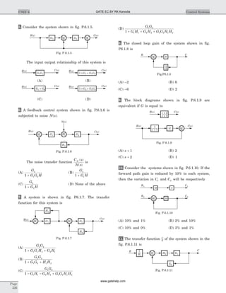
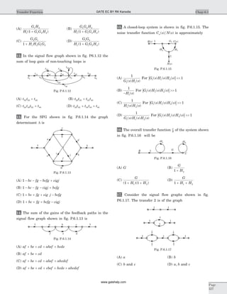
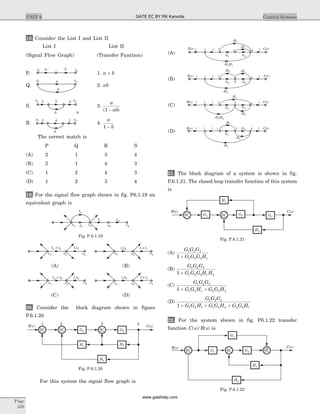
![(A)
G
H G H G G G H
3
1 2 2 3 1 2 21 - - -
(B)
G G G
H G H G G G H
3 1 2
1 2 2 3 1 2 21
+
+ + +
(C)
G
H G H G G G H
3
1 2 2 3 1 2 21 + + +
(D)
G
H G H G G G H
3
1 2 2 3 1 2 21 - - -
23. In the signal flow graph shown in fig. P6.1.23 the
transfer function is
‘(A) 3.75 (B) -3
(C) 3 (D) -3.75
24. In the signal flow graph shown in fig. P6.1.24 the
gain C R is
(A)
44
23
(B)
29
19
(C)
44
19
(D)
29
11
25. The gain C s R s( ) ( ) of the signal flow graph shown in
fig. P.6.1.25 is
(A)
G G G G
G G H G G H G
1 2 2 3
1 2 1 2 3 1 41
+
+ + +
(B)
G G G G
G G H G G H G
1 2 2 3
1 3 1 2 3 1 41
+
+ + -
(C)
G G G G
G G H G G H G
1 3 2 3
1 3 1 2 3 1 41
+
+ + -
(D)
G G G G
G G H G G H G
1 3 2 3
1 3 1 2 3 1 41
+
+ + +
26. The transfer function of the system shown in fig.
P.6.1.26 is
(A)
G G
G G H G G H
1 2
1 2 1 1 2 21 - -
(B)
G G
G H G G H
1 2
2 2 1 2 11 - -
(C)
G G
G H G G H H
1 2
2 2 1 2 1 21 - +
(D)
G G
G G H H
1 2
1 2 1 21 -
27. For the block diagram shown in fig. P.6.1.27
transfer function C s R s( ) ( ) is
(A)
G G
G G G G G G G G G G G G G G
1 2
1 2 1 7 3 1 2 8 6 1 2 3 7 51 + + + +
(B)
G G
G G G G G G G G G G G G G G
1 2
1 4 1 2 8 1 2 5 7 1 2 3 6 71 + + + +
(C)
G G
G G G G G G G G G G G G G G
1 2
1 4 1 2 8 1 2 5 7 1 2 3 6 71
+
+ + + +
(D)
G G
G G G G G G G G G G G G G G G
1 2
1 2 3 6 7 1 3 4 5 1 2 3 6 7 81
+
+ + + +
28. For the block diagram shown in fig. P.6.1.28 the
numerator of transfer function is
(A) G G G G G G6 4 3 5 3 2[ ( )]+ + +
(B) G G G G G G6 2 3 5 3 4[ ( )]+ + +
Chap 6.1Transfer Function
Page
329
+
H2H1
G1 G2
R s( ) C s( )+
+
Fig. P.6.1.26
+
G3G1 G2
G4 G5 G6
G7
G8
+
+
+
+
R s( )
C s( )
Fig. P.6.1.27
G3
G2G1
G4
-H1
1 1R s( ) C s( )
Fig. P.6.1.25
R C
-1 -1 -1
5
2 3 4
11
Fig. P.6.1.24
R C235
-3
Fig. P.6.1.23
G2 G5 G6
+
+
+
+
+
G3
G1
G4
+
+
R s( ) C s( )
Fig. P.6.1.28
GATE EC BY RK Kanodia
www.gatehelp.com](https://image.slidesharecdn.com/a-150815031147-lva1-app6892/85/A-gate-by-rk-kanodia-210-320.jpg)
![(C) G G G G G G6 1 2 3 4 5[ ( )]+ + +
(D) None of the above
29. For the block diagram shown in fig. P.6.1.29 the
transfer function C s R s( ) ( ) is
(A)
50 2
150 1003 2
( )s
s s s
-
+ + -
(B)
50 2
1503 2
( )s
s s s
-
+ +
(C)
50
150 1003 2
s
s s s+ + -
(D)
50
1502
s s+ +
30. For the SFG shown in fig. P.6.1.30 the transfer
function C
R
is
(A)
G G G
G H G H G H
1 2 3
1 1 2 2 3 31
+ +
+ + +
(B)
G G G
G H G H G H G G H H
1 2 3
1 1 2 2 3 3 1 3 1 31
+ +
+ + + +
(C)
G G G
G H G H G H
1 2 3
1 1 2 2 3 31 + + +
(D)
G G G
G H G H G H G G H H
1 2 3
1 1 2 2 3 3 1 3 1 31 + + + +
31. Consider the SFG shown in fig. P6.1.31. The D for
this graph is
(A) 1 1 1 2 3 3 1 3 2+ + +G H G G H G G H
(B) 1 1 1 2 3 3 1 3 3 2 4 2 3+ - - +G H G G H G G H G G H H
(C) 1 1 1 2 3 3 1 3 3 2 4 2 3+ + + -G H G G H G G H G G H H
(D) 1 1 1 2 3 3 1 3 3 2 4 2 3+ + + +G H G G H G G H G G H H
32. The transfer function of the system shown in fig.
P.6.1.32 is
(A)
G G G G
G H G G
2 3 1 3
3 1 2 31
+
- +
(B)
G G G G
G H G G
2 3 1 3
3 1 2 31
+
+ -
(C)
G G G G
G H G G
2 3 1 3
3 1 2 31
+
+ +
(D)
G G G G
G H G G
2 3 1 3
3 1 2 31
+
- -
33. The closed loop transfer function of the system
shown in fig. P6.1.33 is
(A)
G G G G G G G G
G G G H H H G H H H G H
1 2 3 2 3 4 1 4
1 3 4 1 2 3 2 4 1 2 4 11
+ +
+ + +
(B)
G G G G G
G G H H H G H G G H H
2 4 1 2 3
1 3 1 2 3 4 1 3 4 1 21
+
+ + +
(C)
G G G G G
G G H H G H G G H H
1 3 4 2 4
3 4 1 2 4 1 1 3 3 21
+
+ + +
(D)
G G G G G G G G
G G G H H H G G H H G H
1 3 4 2 3 4 2 4
1 3 4 1 2 3 3 4 1 2 4 11
+ +
+ + +
Statement for Q.34-37:
A block diagram of feedback control system is
shown in fig. P6.1.34-37
34. The transfer function
C
R R
1
1 02 =
is
(A)
G
G1 2 2
-
(B)
G G
G
( )1
1 2 2
-
-
(C)
G G
G
( )1 2
1 2
-
-
(D)
G
G1 2
-
Page
330
UNIT 6 Control Systems
G1
G2 G3
-H1
-H2
-H3
R C1
G4
1
Fig. P.6.1.31
CR
H1
G1
G2
+ G3
+
+
Fig. P.6.1.32
+
+
H2 H1H3
G1
G2
+ G3
+
+
G4
CR
Fig. P.6.1.33
CR G1
G2
-H3-H2-H1
G3 1
Fig. P.6.1.30
R s1( ) C s1( )
G
+
R s2( ) C s2( )
G+
+
+
+
Fig. P.6.1.34-37
GATE EC BY RK Kanodia
www.gatehelp.com](https://image.slidesharecdn.com/a-150815031147-lva1-app6892/85/A-gate-by-rk-kanodia-211-320.jpg)

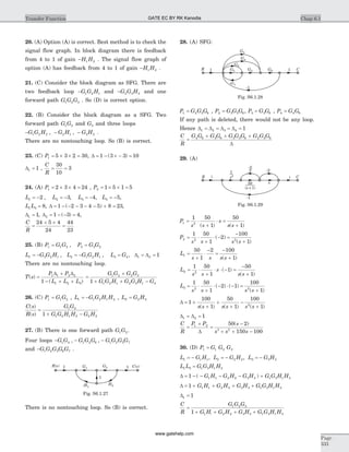
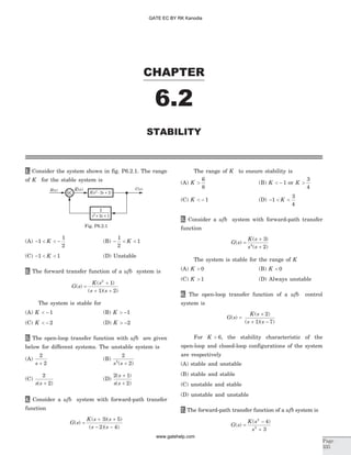
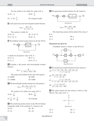
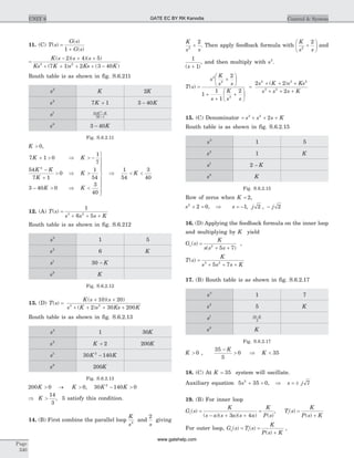
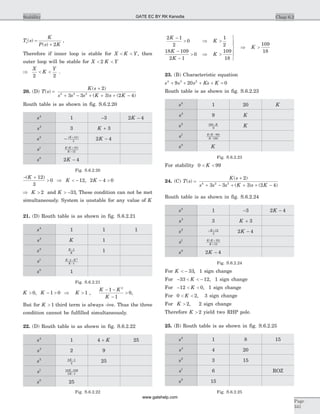
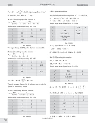
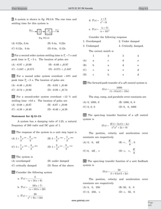
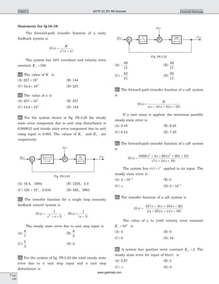
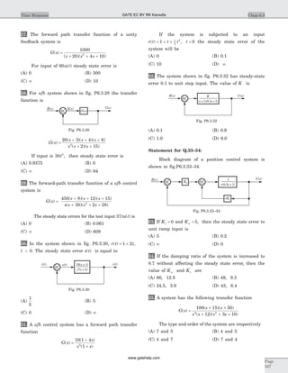
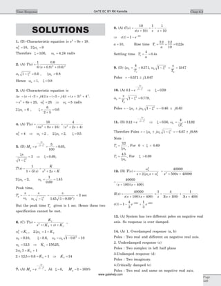
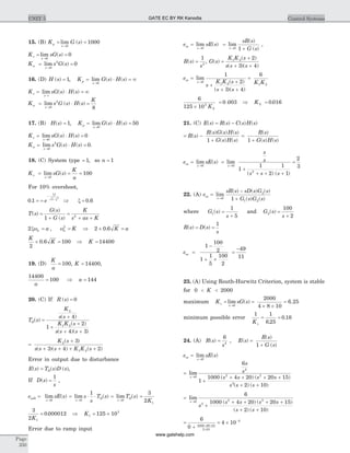
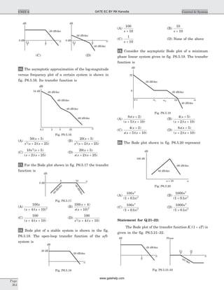
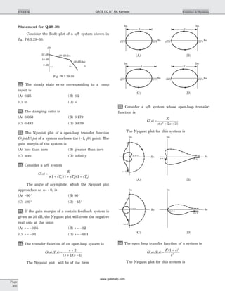
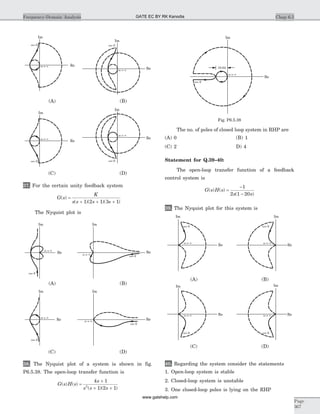
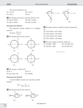
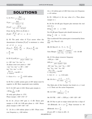

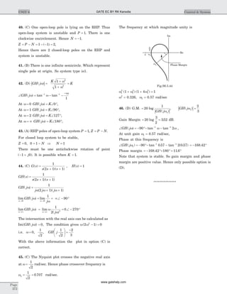
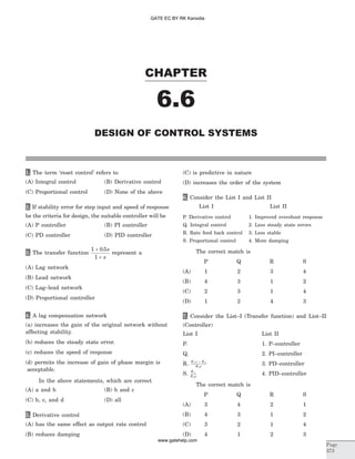

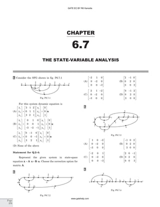
![(A)
0 1 4
1 0 0
3 0 0
-
-
é
ë
ê
ê
ê
ù
û
ú
ú
ú
(B)
0 1 4
1 0 0
3 0 0
-
-
é
ë
ê
ê
ê
ù
û
ú
ú
ú
(C)
-
-
é
ë
ê
ê
ê
ù
û
ú
ú
ú
4 1 0
0 0 1
0 0 3
(D)
4 1 0
0 0 1
0 0 3
-
-
é
ë
ê
ê
ê
ù
û
ú
ú
ú
5. The state equation of a LTI system is represented by
&x x u=
- -
é
ë
ê
ù
û
ú +
é
ë
ê
ù
û
ú
0 1
2 1
0 1
1 0
The Eigen values are
(A) - +1 1, (B) - ±0 5 1 323. .j
(C) - -1 1, (D) None of the above
6. The state equation of a LTI system is
&x x u=
-
-
é
ë
ê
ù
û
ú +
é
ë
ê
ù
û
ú
3 0
0 3
0
1
The state-transition matrix F( )t is
(A)
e
e
t
t
-
-
é
ë
ê
ù
û
ú
3
3
0
0
(B)
-é
ë
ê
ù
û
ú
-
-
e
e
t
t
3
3
0
0
(C)
-
-
é
ë
ê
ù
û
ú
-
-
e
e
t
t
3
3
0
0
(D)
e
e
t
t
-
-
-
é
ë
ê
ù
û
ú
3
3
0
0
7. The state equation of a LTI system is
&x x u=
-
é
ë
ê
ù
û
ú +
é
ë
ê
ù
û
ú
0 2
2 0
0
1
The state transition matrix is
(A)
cos sin
sin cos
2 2
2 2
t t
t t-
é
ë
ê
ù
û
ú (B)
cos sin
sin cos
2 2
2 2
t t
t t
-é
ë
ê
ù
û
ú
(C)
sin cos
cos sin
2 2
2 2
t t
t t-
é
ë
ê
ù
û
ú (D)
sin cos
cos sin
2 2
2 2
t t
t t
-é
ë
ê
ù
û
ú
Statement for Q.8–9:
The state-space representation of a system is given
by & ( ) ( ) ( )x A x B ut t t= × + × , where
A =
-
é
ë
ê
ù
û
ú
0 2
2 0
, B =
é
ë
ê
ù
û
ú
0
1
If x( )0 is the initial state vector, and the
component of the input vector u( )t are all unit step
function, then the state transition equation is given by
& ( ) ( )x xt t t= +F( ) ( )0 q , where F( )t is a state transition
matrix and q( )t is a vector matrix.
8. The F( )t is
(A)
cos sin
sin cos
2 2
2 2
t t
t t-
é
ë
ê
ù
û
ú (B)
cos sin
sin cos
2 2
2 2
t t
t t
-é
ë
ê
ù
û
ú
(C)
sin cos
cos sin
2 2
2 2
t t
t t-
é
ë
ê
ù
û
ú (D)
sin cos
cos sin
2 2
2 2
t t
t t
-é
ë
ê
ù
û
ú
9. The q( )t is
(A)
0 5 1 2
0 5 2
. ( sin )
. cos
-é
ë
ê
ù
û
ú
t
t
(B)
sin
cos
2
2
t
t
é
ë
ê
ù
û
ú
(C)
0 5 1 2
0 5 2
. ( cos )
. sin
-é
ë
ê
ù
û
ú
t
t
(D)
cos
sin
2
2
t
t
é
ë
ê
ù
û
ú
10. From the following matrices, the state-transition
matrices can be
(A)
-
-
é
ë
ê
ù
û
ú
-
-
e
e
t
t
0
0 1
(B)
1 0
0
-é
ë
ê
ù
û
ú
-
-
e
e
t
t
(C)
1 0
1 -
é
ë
ê
ù
û
ú- -
e et t
(D)
1
0
-é
ë
ê
ù
û
ú
- -
-
e e
e
t t
t
Statement for Q.11–13:
A system is described by the dynamic equations
& ( ) ( ) ( )x A x B ut t t= × + × , y t t( ) ( )= ×C x where
A =
- - -
é
ë
ê
ê
ê
ù
û
ú
ú
ú
0 1 0
0 0 1
1 2 3
, B =
é
ë
ê
ê
ê
ù
û
ú
ú
ú
0
0
1
, C = [ ]1 0 0
11. The Eigen values of A are
(A) 0.325, -1.662 ± j0.562
(B) 2.325, 0.338 ± j0.562
(C) -2.325, -0.338 ± j0.562
(D) -0.325, 1.662 ± j0.562
12. The transfer-function relation between X s( ) and
U s( ) is
(A)
1
3 2 1
1
3 2
2s s s
s
s
+ + -
-
é
ë
ê
ê
ê
ù
û
ú
ú
ú
(B)
1
3 2 1
1
3 2
2s s s
s
s
+ + +
é
ë
ê
ê
ê
ù
û
ú
ú
ú
(C)
1
3 2 1
1
3 2
2s s s
s
s
+ + +
-
é
ë
ê
ê
ê
ù
û
ú
ú
ú
(D) None of the above
13. The output transfer function Y s U s( ) ( ) is
(A) s s s s( )3 2 1
3 2 1+ + + -
(B) s s s s( )3 2 1
3 2 1+ + - -
(C) ( )s s s3 2 1
3 2 1+ + + -
(D) None of the above
Chap 6.7The State-Variable Analysis
Page
377
GATE EC BY RK Kanodia
www.gatehelp.com](https://image.slidesharecdn.com/a-150815031147-lva1-app6892/85/A-gate-by-rk-kanodia-241-320.jpg)
![14. A system is described by the dynamic equation
& ( ) ( ) ( )x A x B ut t t= × + × , y t t( ) ( )= ×C x where
A =
-
-
é
ë
ê
ù
û
ú
1 0
0 2
, B =
é
ë
ê
ù
û
ú
1
0
and C = [ ]1 1
The output transfer function Y s U s( ) ( ) is
(A)
( )
( )
s
s
+
+
1
2 2
(B)
s
s
+
+
1
2
(C)
( )
( )
s
s
+
+
2
1
(D) None of the above
15. The state-space representation of a system is given
by
& ( ) ( ) ( )x x ut t t=
-
-
é
ë
ê
ù
û
ú +
é
ë
ê
ù
û
ú
1 0
0 2
1
1
, y t t( ) [ ] ( )= 1 1 x
The transfer function of this system is
(A) ( )s s2 1
3 2+ + -
(B) ( )s + -
2 1
(C) s s s( )2 1
3 2+ + -
(D) ( )s + -
1 1
16. The state-space representation for a system is
&x x u=
- - -
é
ë
ê
ê
ê
ù
û
ú
ú
ú
+
é
ë
ê
ê
ê
ù
û
ú
ú
ú
0 1 0
0 0 1
1 2 3
10
0
0
, y = [ ]1 0 0 x
The transfer function Y s U s( ) ( ) is
(A)
10 2 3 1
3 2 1
2
3 2
( )s s
s s s
+ +
+ + +
(B)
10 2 3 1
2 3 1
2
3 2
( )s s
s s s
+ +
+ + +
(C)
10 2 3 2
3 2 1
2
3 2
( )s s
s s s
+ +
+ + +
(D)
10 2 3 2
2 3 1
2
3 2
( )s s
s s s
+ +
+ + +
Statement for Q.17–18:
Determine the state-space representation for the
transfer function given in question. Choose the state
variable as follows
x c y1 = = , x
dc
dt
c2 = = & , x
d c
dt
c3
2
2
= = && , x
d c
dt
c4
3
2
= =&&&
17.
C s
R s s s s
( )
( )
=
+ + +
24
9 26 243 2
(A)
&
&
&
x
x
x
x
x
x
1
2
3
1
2
3
0 1 0
0 0 1
24 26 9
é
ë
ê
ê
ê
ù
û
ú
ú
ú
=
- - -
é
ë
ê
ê
ê
ù
û
ú
ú
ú
é
ë
ê
ê
ê
ù
û
ú
ú
ú
+
é
ë
ê
ê
ê
ù
û
ú
ú
ú
0
0
24
r
(B)
&
&
&
x
x
x
x
x
x
1
2
3
1
2
3
0 1 0
0 0 1
24 26 9
é
ë
ê
ê
ê
ù
û
ú
ú
ú
=
é
ë
ê
ê
ê
ù
û
ú
ú
ú
é
ë
ê
ê
ê
ù
û
ú
ú
ú
+
é
ë
ê
ê
ê
ù
û
ú
ú
ú
0
0
24
r
(C)
&
&
&
x
x
x
x
x
x
1
2
3
1
2
3
0 1 0
0 0 1
9 26 24
é
ë
ê
ê
ê
ù
û
ú
ú
ú
=
é
ë
ê
ê
ê
ù
û
ú
ú
ú
é
ë
ê
ê
ê
ù
û
ú
ú
ú
+
é
ë
ê
ê
ê
ù
û
ú
ú
ú
0
0
24
r
(D)
&
&
&
x
x
x
x
x
x
1
2
3
1
2
3
0 1 0
0 0 1
9 26 24
é
ë
ê
ê
ê
ù
û
ú
ú
ú
=
- - -
é
ë
ê
ê
ê
ù
û
ú
ú
ú
é
ë
ê
ê
ê
ù
û
ú
ú
ú
+
é
ë
ê
ê
ê
ù
û
ú
ú
ú
0
0
24
r
18.
C s
R s s s s s
( )
( )
=
+ + + +
100
20 10 7 1004 3 2
(A) &x x=
é
ë
ê
ê
ê
ê
ù
û
ú
ú
ú
ú
+
é
ë
ê
ê
ê
ê
ù0 1 0 0
0 0 1 0
0 0 0 1
100 7 10 20
0
0
0
100û
ú
ú
ú
ú
r,
y = [ ]1 0 0 0 x
(B) &x x=
- - - -
é
ë
ê
ê
ê
ê
ù
û
ú
ú
ú
ú
+
é
ë
ê
0 1 0 0
0 0 1 0
0 0 0 1
100 7 10 20
0
0
0
100
ê
ê
ê
ù
û
ú
ú
ú
ú
r
y = [ ]1 0 0 0 x
(C) &x x=
é
ë
ê
ê
ê
ê
ù
û
ú
ú
ú
ú
+
é
ë
ê
ê
ê
ê
ù
û
ú
0 1 0 0
0 0 1 0
0 0 0 1
20 10 7 100
0
0
0
1
ú
ú
ú
r
y = [ ]100 0 0 0 x
(D) &x x=
- - - -
é
ë
ê
ê
ê
ê
ù
û
ú
ú
ú
ú
+
é
ë
ê
ê
ê
0 1 0 0
0 0 1 0
0 0 0 1
20 10 7 100
0
0
0
1ê
ù
û
ú
ú
ú
ú
r
y = [ ]100 0 0 0 x
19. A state-space representation of a system is given by
&x x=
-
é
ë
ê
ù
û
ú
0 1
2 0
, y = -[ ]1 1 x, and x( )0
0
1
=
é
ë
ê
ù
û
ú
The time response of this system will be
(A) sin 2t (B)
3
2
2sin t
(C) -
1
2
2sin t (D) 3 2sin t
20. For the transfer function
Y s
U s
s
s s
( )
( ) ( )( )
=
+
+ +
3
1 2
The state model is given by &x A x B u= × + × ,
y = ×C x. The A , B, C are
Page
378
UNIT 6 Control & SystemGATE EC BY RK Kanodia
www.gatehelp.com](https://image.slidesharecdn.com/a-150815031147-lva1-app6892/85/A-gate-by-rk-kanodia-242-320.jpg)
![29. &x x r=
- - -
- -
- -
é
ë
ê
ê
ê
ù
û
ú
ú
ú
+
é
ë
ê
ê
ê
ù
û
ú
ú
ú
5 4 2
3 10 0
1 1 5
1
1
0
, y = -[ ]1 2 1 x
estep( )¥ eramp( )¥
(A) 1.0976 0
(B) 1.0976 ¥
(C) 0 1.0976
(D) ¥ 1.0976
30. &x x r= - -
-
é
ë
ê
ê
ê
ù
û
ú
ú
ú
+
é
ë
ê
ê
ê
ù
û
ú
ú
ú
0 1 0
5 9 7
1 0 0
0
0
1
, y = [ ]1 0 0 x
estep ( )¥ eramp ( )¥
(A) 0 0.714
(B) ¥ 0.714
(C) 0 4.86
(D) ¥ 4.86
Statement for Q.31–33:
Consider the system shown in fig. P6.7.31-33
31. The controllability matrix is
(A)
1 0
0 1
é
ë
ê
ù
û
ú (B)
1 2
2 4
-
-
é
ë
ê
ù
û
ú
(C)
1 0
0 1-
é
ë
ê
ù
û
ú (D)
1 2
2 4- -
é
ë
ê
ù
û
ú
32. The observability matrix is
(A)
1 0
0 1
é
ë
ê
ù
û
ú (B)
1 2
2 4
-
-
é
ë
ê
ù
û
ú
(C)
1 0
0 1-
é
ë
ê
ù
û
ú (D)
1 2
2 4- -
é
ë
ê
ù
û
ú
33. The system is
(A) Controllable and observable
(B) Controllable only
(C) Observable only
(D) None of the above
Statement for Q.34–36:
Consider the system shown in fig. P6.7.34-36.
34. The controllability matrix for this system is
(A)
10 10 10
10 0 20
10 20 40
-
- -
-
é
ë
ê
ê
ê
ù
û
ú
ú
ú
(B)
0 1 2
1 1 1
1 2 4
-
-
-
é
ë
ê
ê
ê
ù
û
ú
ú
ú
(C)
10 10 10
10 0 20
10 20 40
-
-
- -
é
ë
ê
ê
ê
ù
û
ú
ú
ú
(D)
0 1 1
1 6 1
1 4 4
-
-
- -
é
ë
ê
ê
ê
ù
û
ú
ú
ú
35. The observability matrix is
(A)
10 10 10
10 0 20
10 10 40
-
- -
-
é
ë
ê
ê
ê
ù
û
ú
ú
ú
(B)
0 1 2
1 1 1
1 2 4
-
-
-
é
ë
ê
ê
ê
ù
û
ú
ú
ú
(C)
10 10 10
10 0 20
10 10 40
-
-
- -
é
ë
ê
ê
ê
ù
û
ú
ú
ú
(D)
0 1 2
1 1 1
1 2 4
-
-
é
ë
ê
ê
ê
ù
û
ú
ú
ú
36. The system is
(A) Controllable and observable
(B) Controllable only
(C) Observable only
(D) None of the above
Statement for Q.37–38:
A state flow graph is shown in fig. P6.7.37-38
37. The state and output equation for this system is
(A)
&
&
x
x
x
x
1
2
1
2
0 1
5
21
4
0
1
é
ë
ê
ù
û
ú =
-é
ë
ê
ê
ù
û
ú
ú
é
ë
ê
ù
û
ú +
é
ë
ê
ù
û
úu, y
x
x
=
é
ë
ê
ù
û
ú[ ]5 4 1
2
Page
380
UNIT 6 Control & System
1
1 1-2 x2 x1
y
-5
-6
u
1
s
1
s
Fig. P6.7.31-33
x2 x1
1
1
1
10
y-1
-10
10
-2
x3
u -1
1
s
1
s
1
s
Fig. P6.7.34-36
x2 x1 5
y
-5
u
1
s
-21
4
1
s1
4
Fig. P6.7.37-38
GATE EC BY RK Kanodia
www.gatehelp.com](https://image.slidesharecdn.com/a-150815031147-lva1-app6892/85/A-gate-by-rk-kanodia-243-320.jpg)
![(B)
&
&
x
x
x
x
1
2
1
2
0 1
5
21
4
0
1
é
ë
ê
ù
û
ú =
- -
é
ë
ê
ê
ù
û
ú
ú
é
ë
ê
ù
û
ú +
é
ë
ê
ù
û
úu, y
x
x
=
é
ë
ê
ù
û
ú[ ]5 4 1
2
(C)
&
&
x
x
x
x
1
2
1
2
0 1
5
21
4
1
1
é
ë
ê
ù
û
ú =
-é
ë
ê
ê
ù
û
ú
ú
é
ë
ê
ù
û
ú +
é
ë
ê
ù
û
úu, y
x
x
=
é
ë
ê
ù
û
ú[ ]4 5 1
2
(D)
&
&
x
x
x
x
1
2
1
2
0 1
5
21
4
1
1
é
ë
ê
ù
û
ú =
- -
é
ë
ê
ê
ù
û
ú
ú
é
ë
ê
ù
û
ú +
é
ë
ê
ù
û
úu, y
x
x
=
é
ë
ê
ù
û
ú[ ]4 5 1
2
38. The system is
(A) Observable and controllable
(B) Controllable only
(C) Observable only
(D) None of the above
39. Consider the network shown in fig. P6.7.39. The
state-space representation for this network is
(A)
&
&
.
. .
v
i
v
i
C
L
C
L
é
ë
ê
ù
û
ú =
-
-
é
ë
ê
ù
û
ú
é
ë
ê
ù
û
ú +
é
ë
ê
ù0 25 1
0 5 0
1
0 25û
úvs, i
v
i
R
C
L
=
é
ë
ê
ù
û
ú[ . ]0 5 0
(B)
&
&
.
.
.v
i
v
i
C
L
C
L
é
ë
ê
ù
û
ú =
-
-
é
ë
ê
ù
û
ú
é
ë
ê
ù
û
ú +
é
ë
ê
ù0 5 1
0 25 0
0 25
1 û
úvs, i
v
i
R
C
L
=
é
ë
ê
ù
û
ú[ . ]0 5 0
(C)
&
&
.
.
.v
i
v
i
C
L
C
L
é
ë
ê
ù
û
ú =
é
ë
ê
ù
û
ú
é
ë
ê
ù
û
ú +
é
ë
ê
ù
û
ú
1 0 25
0 0 5
0 25
0
vs, i
v
i
R
C
L
=
é
ë
ê
ù
û
ú[ . ]0 5 0
(D)
&
&
.
.
.v
i
v
i
C
L
C
L
é
ë
ê
ù
û
ú =
-
-
é
ë
ê
ù
û
ú
é
ë
ê
ù
û
ú +
é
ë
ê
ù1 0 25
0 0 5
0 25
0 û
úvs, i
v
i
R
C
L
=
é
ë
ê
ù
û
ú[ . ]0 5 0
40. For the network shown in fig. P6.7.40. The output is
i tR ( ). The state space representation is
(A)
&
&
v
i
v
i
vi
1
3
1
1
1 1
3 1
1
0
é
ë
ê
ù
û
ú =
-
-
é
ë
ê
ù
û
ú
é
ë
ê
ù
û
ú +
é
ë
ê
ù
û
ú , i
v
i
R =
é
ë
ê
ù
û
ú[ ]4 1 1
3
(B)
&
&
v
i
v
i
vi
1
3
1
3
1 1
3 1
1
0
é
ë
ê
ù
û
ú =
- -
- -
é
ë
ê
ù
û
ú
é
ë
ê
ù
û
ú +
é
ë
ê
ù
û
ú , i
v
i
R =
é
ë
ê
ù
û
ú[ ]4 1 1
3
(C)
&
&
v
v
v
v
vi
1
2
1
2
1 3
1 6
1
1
é
ë
ê
ù
û
ú =
-é
ë
ê
ù
û
ú
é
ë
ê
ù
û
ú +
-
é
ë
ê
ù
û
ú , i
v
v
R =
é
ë
ê
ù
û
ú[ ]1 4 1
2
(D)
&
&
v
v
v
v
vi
1
2
1
2
1 3
1 6
1
1
é
ë
ê
ù
û
ú =
-
é
ë
ê
ù
û
ú
é
ë
ê
ù
û
ú +
-
é
ë
ê
ù
û
ú , i
v
v
R =
é
ë
ê
ù
û
ú[ ]1 4 1
2
Statement for Q.41–43:
Consider the network shown in fig. P6.7.41-43.
This system may be represented in state space
representation &x A x B u= × + ×
41. The state variable may be
(A) i iR R1 2, (B) i iL C,
(C) v iC L, (D) None of the above
42. If state variable are chosen as in previous question,
then the matrix A is
(A)
1 1
1 3
-
-
é
ë
ê
ù
û
ú (B)
1 3
1 1
-
-
é
ë
ê
ù
û
ú
(C)
-
-
é
ë
ê
ù
û
ú
1 3
1 1
(D)
3 1
1 1
-
-
é
ë
ê
ù
û
ú
43. The matrix B is
(A)
3
1-
é
ë
ê
ù
û
ú (B)
-é
ë
ê
ù
û
ú
1
3
(C)
-é
ë
ê
ù
û
ú
3
1
(D)
1
3-
é
ë
ê
ù
û
ú
Statement for Q.44–47:
Consider the network shown in fig. P6.7.44-47
Chap 6.7The State-Variable Analysis
Page
381
iL 4 H
iR
iC
1 F2 Wvs
Fig. P6.7.39
i1
iR
v2
1 F 1 W
1 H1 W
vi
i3
4v1
v1
i2
Fig. P6.7.40
is 1 W
iR1 iL
F
iC
iR2
1 W 4vL
1
2
Fig. P6.7.41-43
vi
i2
i3
i4
i1 1 W
1 H 1 H 1 F
-
+
vo
i51 W 1 W
Fig. P6.7.44-47
GATE EC BY RK Kanodia
www.gatehelp.com](https://image.slidesharecdn.com/a-150815031147-lva1-app6892/85/A-gate-by-rk-kanodia-244-320.jpg)
![44. The state variable may be
(A) i i2 4, (B) i i vo2 4, ,
(C) i i1 3, (D) i i i1 3 5, ,
45. In state space representation matrix A is
(A)
- -
- -
- - -
é
ë
ê
ê
ê
ê
ê
ê
ù
û
ú
ú
ú
ú
ú
ú
2
3
1
3
1
3
1
3
2
3
2
3
1
3
2
3
1
3
(B)
1
3
1
3
2
3
2
3
2
3
1
3
1
3
2
3
1
3
- -
- -
- - -
é
ë
ê
ê
ê
ê
ê
ê
ù
û
ú
ú
ú
ú
ú
ú
(C)
2
3
1
3
1
3
1
3
2
3
2
3
1
3
2
3
1
3
- -
- -
é
ë
ê
ê
ê
ê
ê
ê
ù
û
ú
ú
ú
ú
ú
ú
(D)
- -
- -
- - -
é
ë
ê
ê
ê
ê
ê
ê
ù
û
ú
ú
ú
ú
ú
ú
1
3
1
3
2
3
2
3
2
3
1
3
1
3
2
3
1
3
46. The matrix B is
(A)
2
3
1
3
1
3
-
-
é
ë
ê
ê
ê
ê
ê
ê
ù
û
ú
ú
ú
ú
ú
ú
(B)
2
3
1
3
1
3
é
ë
ê
ê
ê
ê
ê
ê
ù
û
ú
ú
ú
ú
ú
ú
(C)
-
-
é
ë
ê
ê
ê
ê
ê
ê
ù
û
ú
ú
ú
ú
ú
ú
1
3
1
3
1
3
(D)
2
3
1
3
2
3
é
ë
ê
ê
ê
ê
ê
ê
ù
û
ú
ú
ú
ú
ú
ú
47. If output is vo , then matrix C is
(A) [-1 0 0] (B) [1 0 0]
(C) [0 0 -1] (D) [0 0 1]
************************
SOLUTIONS
1. (B) From the SFG
&x x x x u3 1 2 33 2= - - - +
x
x
s
2
3
= Þ &x x2 3=
x
x
s
1
2
= Þ &x x1 2=
2. (A) &x x x1 1 32= - + , &x x u2 22= - + , &x x u3 33= - +
&
&
&
x
x
x
x
x
x
1
2
3
1
2
3
2 1 0
0 2 0
0 0 3
é
ë
ê
ê
ê
ù
û
ú
ú
ú
=
-
-
-
é
ë
ê
ê
ê
ù
û
ú
ú
ú
é
ë
ê
ê
ê
ù
û
ú
ú
ú
+
é
ë
ê
ê
ê
ù
û
ú
ú
ú
0
0
1
u
3. (C) &x x x1 1 32= - + , &x x u2 22= - + , &x x u3 33= - +
y x x x= + +5 5 51 2 3
&
&
&
x
x
x
x
x
x
1
2
3
1
2
3
2 0 1
0 2 0
0 0 3
é
ë
ê
ê
ê
ù
û
ú
ú
ú
=
-
-
-
é
ë
ê
ê
ê
ù
û
ú
ú
ú
é
ë
ê
ê
ê
ù
û
ú
ú
ú
+
é
ë
ê
ê
ê
ù
û
ú
ú
ú
0
1
1
u
4. (C) &x x x1 1 24= - + , &x x u2 3 2= + , &x x u3 33= - +
&
&
&
x
x
x
x
x
x
1
2
3
1
2
3
4 1 1
0 0 1
0 0 3
é
ë
ê
ê
ê
ù
û
ú
ú
ú
=
-
-
é
ë
ê
ê
ê
ù
û
ú
ú
ú
é
ë
ê
ê
ê
ù
û
ú
ú
ú
+
é
ë
ê
ê
ê
ù
û
ú
ú
ú
0
2
1
u
5. (B) | |Ds s s s= - = + + =I A 2
2 0 Þ = - ±s j0 5 1 323. .
6. (A) ( )s
s
s
I A- =
+
+
é
ë
ê
ù
û
ú
3 0
0 3
, |
( )
s |
s
I A- =
+
1
3 2
( )s s
s
I A- = +
+
é
ë
ê
ê
ê
ù
û
ú
ú
ú
-1
1
3
0
0
1
3
F( ) =t s
e
e
t
t
L 1-
-
-
- ==
é
ë
ê
ù
û
ú{( )}I A
3
3
0
0
7. (A) ( )s
s
s
I A- =
-é
ë
ê
ù
û
ú
2
2
, | |s sI A- = +2
4
( )s
s
s
s
s
s s
s
s
s
I A- =
+ -
é
ë
ê
ù
û
ú = + +
-
+ +
é
ë
ê-1
2
2 2
2 2
1
4
2
2
4
2
4
2
4 4
ê
ê
ù
û
ú
ú
ú
F( ) =t s
t t
t t
L 1-
- =
-
é
ë
ê
ù
û
ú{( )}
cos sin
sin cos
I A
2 2
2 2
8. (A) ( )s
s
s
I A- =
-é
ë
ê
ù
û
ú
2
2
, Ds s s= - = +| |I A 2
4
Page
382
UNIT 6 Control & SystemGATE EC BY RK Kanodia
www.gatehelp.com](https://image.slidesharecdn.com/a-150815031147-lva1-app6892/85/A-gate-by-rk-kanodia-245-320.jpg)
![( )s
s
s
s
s
s s
s
s
s
I A- =
+ -
é
ë
ê
ù
û
ú = + +
-
+ +
é
ë
ê-1
2
2 2
2 2
1
4
2
2
4
2
4
2
4 4
ê
ê
ù
û
ú
ú
ú
F( ) =t s
t t
t t
L 1-
- =
-
é
ë
ê
ù
û
ú{( )}
cos sin
sin cos
I A
2 2
2 2
9. (C) q( ) {( ) ( )}t s R s= -- -
L 1 1
I A B
=
+ -
é
ë
ê
ù
û
ú
é
ë
ê
ù
û
ú
é
ë
ê
ù
û
ú
ì
í
î
ü
ý
þ
-
L 1
2
1
4
2
2
0
1
1
1
1
s
s
s s
=
+
é
ë
ê
ù
û
ú
ì
í
î
ü
ý
þ
-
L 1
2
1
4
2
s s s( )
= +
+
é
ë
ê
ê
ê
ù
û
ú
ú
ú
ì
í
ïï
î
ï
ï
ü
ý
ïï
þ
ï
ï
-
L 1
2
2
2
4
1
4
s s
s
( )
( )
=
-é
ë
ê
ù
û
ú
0 5 1 2
0 5 2
. ( cos )
. sin
t
t
10. (C) (A) is not a state-transition matrix, since F( )0 ¹ I
(B) is not a state-transition matrix since F( )0 ¹ I
(C) is a state-transition matrix since F( )0 = I and
[ ( )] ( )F Ft t-
= -1
11. (C) ( )s
s
s
s
I A- =
-
-
+
é
ë
ê
ê
ê
ù
û
ú
ú
ú
1 0
0 1
1 2 3
| |s s s sI A- = + + +3 2
3 2 1,
Þ = - - ±s j2 325 0 338 0 562. , . .
12. (B)
X s
U s
s
( )
( )
( )= - -
I A B1
=
+ + +
+ + +
- +
- - -
é
ë
ê
ê
ê
ù
û
ú1
3 2 1
3 2 3 1
1 3
2 1
3 2
3
2s s s
s s s
s s s
s s s
( )
ú
ú
é
ë
ê
ê
ê
ù
û
ú
ú
ú
0
0
1
=
+ + +
é
ë
ê
ê
ê
ù
û
ú
ú
ú
1
3 2 1
1
3 2
2s s s
s
s
13. (C)
Y s
U s
CX s
U s
( )
( )
( )
( )
=
=
+ + +
+ + +
+ + +
é
ë
ê
ê
ê
ê
ê
[ ]1 0 0
1
3 2 1
3 2 1
3 2 1
3 2
3 2
2
3 2
s s s
s
s s s
s
s s sê
ù
û
ú
ú
ú
ú
ú
ú
=
+ + +
1
3 2 13 2
s s s
14. (D)
Y s
U s
s
( )
( )
( )= - -
C I A B1
B =
+
+
é
ë
ê
ù
û
ú
é
ë
ê
ù
û
ú =
+
+
[ ]
( )
1 1
1 1 1
0 1
0
1
2
1 2
Ds
s
s
s
s
15. (D) T s s( ) ( )=
é
ë
ê
ù
û
ú -
é
ë
ê
ù
û
ú
-1
1
1
0
1
I A
( )s s
s
I A- = +
+
é
ë
ê
ê
ê
ù
û
ú
ú
ú
-1
1
1
0
0
1
2
T s s
s
s
( ) =
é
ë
ê
ù
û
ú
+
+
é
ë
ê
ê
ê
ù
û
ú
ú
ú
é
ë
ê
ù
û
ú =
+
1
1
1
1
0
0
1
2
1
0
1
1
16. (C) &x A x B u= × + × , y = × +C x Du
A =
- - -
é
ë
ê
ê
ê
ù
û
ú
ú
ú
0 1 0
0 0 1
1 2 3
, B =
é
ë
ê
ê
ê
ù
û
ú
ú
ú
10
0
0
, C = [ ]1 0 0 , D = 0
T s
Y s
U s
s( )
( )
( )
( )= = - +-
C I A B D1
( ) ( )s
s s s
s s s
s s s
s s s
I A- =
+ + +
+ + +
- +
- - -
-1
3 2
3
2
1
3 2 1
3 2 3 1
1 3
2 1
é
ë
ê
ê
ê
ù
û
ú
ú
ú
Substituting the all values,
T s
s s
s s s
( )
( )
=
+ +
+ + +
10 2 3 2
3 2 1
2
3 2
17. (A)
C s
R s
b
s a s a s a s s s
( )
( ) ( )
=
+ + +
=
+ + +
0
3
2
2
1 0
3 2
24
9 26 24
( ) ( ) ( )s a s a s a C s b R s3
2
2
1 0 0+ + + =
Taking the inverse Laplace transform assuming zero
initial conditions
&&& && &c a c a c a c b r+ + + =2 1 0 0
x c y x c1 2= = =, & , x c3 = &&
& &x c x1 2= = , & &&x c x2 3= =
& &&& && &x c b r a c a c a c3 0 2 1 0= = - - -
= - - - +a x a x a x b r0 1 1 2 2 3 0 ,
&
&
&
x
x
x a a a
x
x
x
1
2
3 0 1 1
1
2
0 1 0
0 0 1
é
ë
ê
ê
ê
ù
û
ú
ú
ú
=
- - -
é
ë
ê
ê
ê
ù
û
ú
ú
ú 3 0
0
0
é
ë
ê
ê
ê
ù
û
ú
ú
ú
+
é
ë
ê
ê
ê
ù
û
ú
ú
úb
r
a a a b0 1 2 024 26 9 24= = = =, , ,
&
&
&
x
x
x
x
x
x
1
2
3
1
2
3
0 1 0
0 0 1
24 26 9
é
ë
ê
ê
ê
ù
û
ú
ú
ú
=
- - -
é
ë
ê
ê
ê
ù
û
ú
ú
ú
é
ë
ê
ê
ê
ù
û
ú
ú
ú
+
é
ë
ê
ê
ê
ù
û
ú
ú
ú
0
0
24
r
y
x
x
x
=
é
ë
ê
ê
ê
ù
û
ú
ú
ú
[ ]1 0 0
1
2
3
18. (B) Fourth order hence four state variable
Chap 6.7The State-Variable Analysis
Page
383
GATE EC BY RK Kanodia
www.gatehelp.com](https://image.slidesharecdn.com/a-150815031147-lva1-app6892/85/A-gate-by-rk-kanodia-246-320.jpg)
![&x x=
- - - -
é
ë
ê
ê
ê
ê
ù
û
ú
ú
ú
ú
=
é
ë
ê
ê
0 1 0 0
0 0 1 0
0 0 0 1
0
0
0
0 1 2 3 0a a a a b
ê
ê
ù
û
ú
ú
ú
ú
r, y = [ ]1 0 0 0 x
a a a a b0 1 2 3 0100 7 10 20 100= = = = =, , , ,
19. (B) A =
-
é
ë
ê
ù
û
ú
0 1
2 0
, ( )s
s
s
s
I A- =
+ -
é
ë
ê
ù
û
ú
-1
2
1
2
1
2
F( ) =t s
t
t
t t
L 1-
- =
-
é
ë
ê
ê
ê
ù
û
ú
ú
ú
{( )}
cos
sin
sin cos
I A
2
2
2
2 2 2
x x( ) ( )
cos
sin
sin cos
t t
t
t
t t
= =
+
- +
é
ë
ê
ê
ê
ù
û
ú
ú
ú
F( ) 0
2
2
2
2 2 2
y x x t= - =1 2
3
2
2sin
20. (C) Find the transfer function of option
For (A) ,
Y s
U s s
( )
( )
=
-
1
2
,
For (B) ,
Y s
U s s
( )
( )
=
-
1
2
For (C),
Y s
U s s s
s
s
( )
( )
[ ]
( )( )
=
+ +
+
+
é
ë
ê
ù
û
ú
é
ë
ê
ù
û
ú0 1
1
1 2
2 0
2 1
1
1
=
+ +
+
+
é
ë
ê
ù
û
ú[ ]
( )( )
0 1
1
1 2
2
3s s
s
s
=
+
+ +
s
s s
3
1 3( )( )
So (C) is correct option.
21. (C) A =
- -
- -
é
ë
ê
ù
û
ú
2 1
3 5
,
| |s s sI A- = + +2
7 7 Þ s = - -5 79 121. , .
22. (B) ( )s
s
s
s
I A- =
- -
- -
- - -
é
ë
ê
ê
ê
ù
û
ú
ú
ú
2 3
0 6 5
1 4 2
| |s s s sI A- = - - +3 2
8 11 8 Þ s = -9 11 0 53 1 64. , . , .
23. (D) X s s( ) ( ) ( )= - + ×-
I A (x B u)1
0
=
- -
+
é
ë
ê
ù
û
ú
é
ë
ê
ù
û
ú +
é
ë
ê
ù
û
ú +
æ
è
ç
ç
ö
ø
÷
÷
-
s
s s
1 2
3 1
2
1
1
1
3
9
1
2
1
5 9
2 4 21 45
7 12 72 2
3 2
3 2
( )( )s s
s s s
s s s+ +
+ + +
- + -
é
ë
ê
ù
û
ú
Y s X s( ) [ ] ( )= 1 2 =
- + -
+ +
4 10 45 105
5 9
3 2
2 2
s s s
s s( )( )
24. (B) X s s( ) ( ) ( )= - + ×-
I A (x B u)1
0
=
+ +
+
- +
é
ë
ê
ù
û
ú
é
ë
ê
ù
û
ú +
é
ë
ê
ù
û
ú
æ
è
ç
ç
1
1 2
1 0
1 2
1
0
1
1
1
( )( )s s
s
s s
ö
ø
÷
÷
=
+
+
+ +
é
ë
ê
ê
ê
ù
û
ú
ú
ú
( )
( )
( )( )
s
s s
s s s
1
2
1
1 2
Y s X s
s s s
( ) [ ] ( )
( )( )
= =
+ +
0 1
1
1 2
Þ = - +- -
y t e et t
( )
1
2
1
2
2
25. (B) X s s( ) ( ) ( )= - + ×-
I A (x B u)1
0
=
+ -
-
+
é
ë
ê
ê
ê
ù
û
ú
ú
ú
é
ë
ê
ê
ê
ù
û
ú
ú
ú
+
é
ë
ê
ê
ê
-
s
s
s
2 1 0
0 1
0 0 1
0
0
0
1
0
0
1
ù
û
ú
ú
ú
æ
è
ç
ç
ç
ö
ø
÷
÷
÷
1
s
=
+
+
+ +
é
ë
ê
ê
ê
ê
ê
ê
ù
û
ú
ú
ú
ú
ú
ú
1
2
1
2
1
1 2
2
2
s s
s s
s s s
( )
( )
( )( )
Y s( ) [ ]= 1 0 0 , X s
s s
( )
( )
=
+
1
2
y t e t
( ) = - -1
2
1
2
2
26. (D) For a unit step input estep( )¥ = + -
1 1
CA B
A =
-
-
-
é
ë
ê
ê
ê
ù
û
ú
ú
ú
5 1 0
0 2 1
20 10 1
, A-
=
- -
- - -
- -
é
ë
ê
ê
ê
ù
û
ú
ú
ú
1
0 4 0 05 0 05
1 0 25 0 25
2 15 0 5
. . .
. .
. .
estep( ) [ ]
. . .
. .
. .
¥ = + -
- -
- -
- -
1 1 1 0
0 4 0 05 0 05
1 0 25 0 25
2 15 0 5
é
ë
ê
ê
ê
ù
û
ú
ú
ú
é
ë
ê
ê
ê
ù
û
ú
ú
ú
0
0
1
= - =1 0 2 0 8. .
27. (A) estep( )¥ = + -
1 1
CA B, A-
=
- -
é
ë
ê
ê
ù
û
ú
ú
1 2
1
3
1 0
estep( ) [ ]¥ = +
- -
é
ë
ê
ê
ù
û
ú
ú
é
ë
ê
ù
û
ú = - =1 1 1
2
1
3
1 0
0
1
1
1
3
2
3
28. (C) e tramp
t
( ) lim [( ) ( )¥ = + +
®¥
- -
1 1 1 2
CA B C A B]
1
2
3
1
+ =-
CA B , e tramp
t
( ) lim ( )¥ = +
é
ëê
ù
ûú = ¥
®¥
-2
3
1 2
C A B
29. (B) estep( )¥ = + -
1 1
CA B
A =
- - -
- -
- -
é
ë
ê
ê
ê
ù
û
ú
ú
ú
5 4 2
3 10 0
1 1 5
, B =
é
ë
ê
ê
ê
ù
û
ú
ú
ú
1
1
0
, C = -[ ]1 2 1
Page
384
UNIT 6 Control & SystemGATE EC BY RK Kanodia
www.gatehelp.com](https://image.slidesharecdn.com/a-150815031147-lva1-app6892/85/A-gate-by-rk-kanodia-247-320.jpg)
![A-
=
-
- -
- - -
1
0 305 0 134 0 122
0 091 0 140 0 037
0 079 0 055
. . .
. . .
. . 0 232.
é
ë
ê
ê
ê
ù
û
ú
ú
ú
estep( ) . .¥ = + =1 0 0976 10976
e tramp
t
( ) lim [( ) ( )¥ = + + = ¥
®¥
- -
1 1 1 2
CA B C A B]
30. (B) A-
=
-
-
é
ë
ê
ê
ê
ù
û
ú
ú
ú
1
0 0 1
1 0 0
1 286 0 143 0 714. . .
estep( ) [ ]
. . .
¥ = +
-
-
é
ë
ê
ê
ê
ù
û
ú
ú
ú
1 1 0 0
0 0 1
1 0 0
1 286 0 143 0 714
0
0
1
0
é
ë
ê
ê
ê
ù
û
ú
ú
ú
=
(A-
=
- -
-
- - -
é
ë
ê
ê
1 2
1286 0 143 0 714
0 0 1
0 776 0 102 0 776
)
. . .
. . .ê
ù
û
ú
ú
ú
C A B( ) .-
=1 2
0 714, eramp( ) .¥ = 0 714
31. (B) &x x u1 2= + , &x x x u2 2 15 6 2= - - -
&x x=
- -
é
ë
ê
ù
û
ú +
-
é
ë
ê
ù
û
ú
0 1
6 5
1
2
u, A , B=
- -
é
ë
ê
ù
û
ú =
-
é
ë
ê
ù
û
ú
0 1
6 5
1
2
C B ABM = [ ] =
-
é
ë
ê
ù
û
ú - -
é
ë
ê
ù
û
ú -
é
ë
ê
ù
û
ú
é
ë
ê
ù
û
ú =
-
-
é
ë
ê
ù
û
ú
1
2
0 1
6 5
1
2
1 2
2 4
32. (A) y x= 1 , y = [ ]1 0 x ,
C = [ ]1 0 , CA = [ ]1 0 , O
C
CA
M =
é
ë
ê
ù
û
ú =
é
ë
ê
ù
û
ú
1 0
0 1
33. (C) det CM = 0. Hence system is not controllable. det
OM = 1. Hence system is observable.
34. (B) &x x x1 1 2= - + , &x x u2 2= - + , &x x u3 32= - +
&x x=
-
-
-
é
ë
ê
ê
ê
ù
û
ú
ú
ú
+
é
ë
ê
ê
ê
ù
û
ú
ú
ú
1 1 0
0 1 0
0 0 2
0
1
1
u, A B=
-
-
-
é
ë
ê
ê
ê
ù
û
ú
ú
ú
=
é
ë
ê
ê
ê
ù
û
ú
ú
ú
1 1 0
0 1 0
0 0 2
0
1
1
,
AB =
-
-
-
é
ë
ê
ê
ê
ù
û
ú
ú
ú
é
ë
ê
ê
ê
ù
û
ú
ú
ú
= -
-
é
ë
ê
ê
ê
ù1 1 0
0 1 0
0 0 2
0
1
1
1
1
2û
ú
ú
ú
A B2
1 1 0
0 1 0
0 0 2
1
1
2
2
1
4
=
-
-
-
é
ë
ê
ê
ê
ù
û
ú
ú
ú
-
-
é
ë
ê
ê
ê
ù
û
ú
ú
ú
=
-é
ë
ê
ê
ê
ù
û
ú
ú
ú
C B AB A Bm = =
-
-
-
é
ë
ê
ê
ê
ù
û
ú
ú
ú
[ 2
0 1 2
1 1 1
1 2 4
]
35. (A) y x x x= - +10 10 101 2 3 , y = -[ ]10 10 10 x
A =
-
-
-
é
ë
ê
ê
ê
ù
û
ú
ú
ú
1 1 0
0 1 0
0 0 2
, C = -[ ]10 10 10 ,
CA = -
-
-
-
é
ë
ê
ê
ê
ù
û
ú
ú
ú
= -[ ] [ ]10 10 10
1 1 0
0 1 0
0 0 2
10 0 20
CA2
10 0 20
1 1 0
0 1 0
0 0 2
10 10 40= -
-
-
-
é
ë
ê
ê
ê
ù
û
ú
ú
ú
= -[ ] [ ]
O
C
CA
CA
M =
é
ë
ê
ê
ê
ù
û
ú
ú
ú
=
-
- -
-
é
ë
ê
ê
ê
ù
û
ú
ú2
10 10 10
10 0 20
10 10 40ú
36. (A) det detCm =
-
-
-
é
ë
ê
ê
ê
ù
û
ú
ú
ú
= -
0 1 2
1 1 1
1 2 4
1,
Since the determinant is not zero, the 3 3´ matrix is
nonsingular and system is controllable
det detOM =
-
- -
-
é
ë
ê
ê
ê
ù
û
ú
ú
ú
= -
10 10 10
10 0 10
10 20 40
3000
The rank of OM is 3. Hence system is observable.
37. (B) &x x x u2 1 25
21
4
= - - + , &x x1 2= , y x x= +5 41 2
&
&
x
x
x
x
1
2
1
2
0 1
5
21
4
0
1
é
ë
ê
ù
û
ú =
- -
é
ë
ê
ê
ù
û
ú
ú
é
ë
ê
ù
û
ú +
é
ë
ê
ù
û
úu, y
x
x
=
é
ë
ê
ù
û
ú[ ]5 4 1
2
38. (B) O
C
CA
M =
é
ë
ê
ù
û
ú =
-
é
ë
ê
ù
û
ú
5 4
20 1
det OM = 0. Thus system is not observable
C B ABM = =
-
é
ë
ê
ê
ù
û
ú
ú
[ ]
0 1
1
21
4
det CM = -1. Thus system is controllable.
39. (B)
dv
dt
ic
c= ,
di
dt
v
vL L
L= =
4
0 25.
vC and iL are state variable.
i i iL C R= + , i i i i
v
C L R L
C
= - = -
2
, v v vL s C= -
Hence equations are
dv
dt
i
v
v iL
L
C
C L= - = - +
2
0 5.
di
dt
v v v vL
s C C s= - = - +0 25 0 25 0 25. ( ) . .
&
&
.
.
.v
i
v
i
C
L
C
L
é
ë
ê
ù
û
ú =
-
-
é
ë
ê
ù
û
ú
é
ë
ê
ù
û
ú +
é
ë
ê
ù0 5 1
0 25 0
0 25
1 û
úvs,
Chap 6.7The State-Variable Analysis
Page
385
GATE EC BY RK Kanodia
www.gatehelp.com](https://image.slidesharecdn.com/a-150815031147-lva1-app6892/85/A-gate-by-rk-kanodia-248-320.jpg)
![i
v
vR
C
C= =
2
0 5. , i
v
i
R
C
L
=
é
ë
ê
ù
û
ú[ . ]0 5 0
40. (B)
dv
dt
i1
2= ,
di
dt
vL
3
=
Hence v1 and i3 are state variable.
i i i v v ii2 1 3 1 3= - = - -( ) , i v i vi2 1 3= - - +
v v v v iL R= - = -1 2 1 , = - + = - -v i v v i1 3 1 1 34 3( )
dv
dt
v i vi
1
1 3= - - + ,
di
dt
v i3
1 33= - - , y i v iR= = +4 1 3
&
&
v
i
v
i
vi
1
3
1
3
1 1
3 1
1
0
é
ë
ê
ù
û
ú =
- -
- -
é
ë
ê
ù
û
ú
é
ë
ê
ù
û
ú +
é
ë
ê
ù
û
ú , i
v
i
R =
é
ë
ê
ù
û
ú[ ]4 1 1
3
41. (C) Energy storage elements are capacitor and
inductor. vC and iL are available in differential form and
linearly independent. Hence vC and iL are suitable for
state-variable.
42. (B)
1
2
dv
dt
iC
C= Þ
dv
dt
iC
C= 2
1
2
di
dt
vL
L= Þ
di
dt
vL
L= 2
v v vL C R= + 2 = +v iC R2 , i v iC L R+ =4 2
v v i vL C C L= + + 4 , - = +3v v iL C C ...(i)
i i i iC s R L= - -1 , i i
v
iC s
L
L= - -
1
...(ii)
Solving equation (i) and (ii)
- - - = +3 ( )i i i v is L C C C , 2 3 3i v i iC C L s= - +
- = + - -3v v i v iL C s L L , 2v v i iL C L s= - + -
dv
dt
v i iC
C L s= - +3 3 ,
di
dt
v i iL
C L s= - + -
&
&
v
i
v
i
iC
L
C
L
s
é
ë
ê
ù
û
ú =
-
-
é
ë
ê
ù
û
ú
é
ë
ê
ù
û
ú +
-
é
ë
ê
ù
û
ú
1 3
1 1
3
1
43. (A) B =
-
é
ë
ê
ù
û
ú
3
1
44. (B) There are three energy storage elements, hence
3 variable. i i2 4, and vo are available in differentiated
form hence these are state variable.
45. (A)
di
dt
v2
2= ,
di
dt
v4
4= ,
dv
dt
io
= 5
Now obtain v v2 4, and i5 in terms of the state variable
- + + + + =v i i i vi o1 3 5 0
But i i i3 1 2= - and i i i5 3 4= -
- + + - + - + =v i i i i i vi o1 1 2 3 4 0( ) ( )
i i i v vo i1 2 4
2
3
1
3
1
3
1
3
= + - +
v v i i i v vi o i2 1 2 4
2
3
1
3
1
3
2
3
= - = - - + +
i i i i i v vo i3 1 2 2 4
1
3
1
3
1
3
1
3
= - = - + - +
i i i i i v vo i5 3 4 2 4
1
3
2
3
1
3
1
3
= - = - - - +
v i v i i v vo o i4 5 2 4
1
3
2
3
2
3
1
3
= + = - - + +
&
&
&
i
i
vo
2
4
2
3
1
3
1
3
1
3
2
3
2
3
1
3
2
3
1
3
é
ë
ê
ê
ê
ù
û
ú
ú
ú
=
- -
- -
- - -
é
ë
ê
ê
ê
ê
ê
ê
ù
û
ú
ú
ú
ú
ú
ú
é
ë
ê
ê
ê
ù
û
ú
ú
ú
+
é
ë
ê
ê
ê
ê
ê
ê
ù
û
ú
ú
ú
ú
ú
ú
i
i
vo
2
4
2
3
1
3
1
3
vi
A =
- -
- -
- - -
é
ë
ê
ê
ê
ê
ê
ê
ù
û
ú
ú
ú
ú
ú
ú
2
3
1
3
1
3
1
3
2
3
2
3
1
3
2
3
1
3
, 46. (B) B =
é
ë
ê
ê
ê
ê
ê
ê
ù
û
ú
ú
ú
ú
ú
ú
2
3
1
3
1
3
47. (D) vo is state variable
y vo= , y
i
i
vo
= =
é
ë
ê
ê
ê
ù
û
ú
ú
ú
[ ]0 0 1
2
4
********
Page
386
UNIT 6 Control & System
is 1 W
iR1 iL
F
iC
iR2
1 W 4vL
-
+
vC
-
-
+
+
vR2
1
2
vL
Fig. S6.7.42
vi
i2
i3
i4
i1 1 W
1 H 1 H 1 F
-
+
vo
i5v2 v4
1 W 1 W
Fig. S6.7.45
GATE EC BY RK Kanodia
www.gatehelp.com](https://image.slidesharecdn.com/a-150815031147-lva1-app6892/85/A-gate-by-rk-kanodia-249-320.jpg)

![20. The power reflected from an aircraft of complicated
shape that is received by a radar can be described by an
exponential random variable W. The density of W is
f w W
e w
w
W
w W
( ) =
>
<
ì
í
ï
îï
ü
ý
ï
þï
-1
0
0 0
0
0
where W0 is the average amount of received power.
The probability that the received power is larger than
the power received on the average is
(A) e-2
(B) e-1
(C) 1 1
- -
e (D) 1 2
- -
e
Statement for Question 21-23:
Delhi averages three murder per week and their
occurrences follow a poission distribution.
21. The probability that there will be five or more
murder in a given week is
(A) 0.1847 (B) 0.2461
(C) 0.3927 (D) 0.4167
22. On the average, how many weeks a year can Delhi
expect to have no murders ?
(A) 1.4 (B) 1.9
(C) 2.6 (D) 3.4
23. How many weeds per year (average) can the Delhi
expect the number of murders per week to equal or
exceed the average number per week ?
(A) 15 (B) 20
(C) 25 (D) 30
24. A discrete random variable X has possible values
x i ii = =2
1 2 3 4, , , , which occur with probabilities 0.4,
0.25, 0.15, 0.1,. The mean value X E X= [ ] of X is
(A) 6.85 (B) 4.35
(C) 3.96 (D) 1.42
25. The random variable X is defined by the density
f x u x eX
x
( ) ( )=
-1
2
2
The expected value of g X X( ) = 3
is
(A) 48 (B) 192
(C) 36 (D) 72
26. The mean of random variable X is
(A) 1/4 (B) 1/6
(C) 1/3 (D) 1/5
27. The variance of random variable X is
(A) 1/10 (B) 3/80
(C) 5/16 (D) 3/16
28. A Random variable X is uniformly distributed on
the interval (-5, 15). Another random variable Y e
X
=
-
5
is formed. The value of E Y[ ] is
(A) 2 (B) 0.667
(C) 1.387 (D) 2.967
29. A random variable X has X = -3, x2
11= and sX
2
2=
For a new random variable Y x= -2 3, the Y, Y
2
and sY
2
are
(A) 0, 81, 8 (B) - 6, 8, 89
(C) - 9, 89, 8 (D) None of the above
Statement for Question 31-32 :
A joint sample space for two random variable X
and Y has four elements ( , ), ( , ), ( , )1 1 2 2 3 3 and (4, 4).
Probabilities of these elements are 0.1, 0.35, 0.05 and
0.5 respectively.
30. The probability of the event{ . , }X Y£ £2 5 6 is
(A) 0.45 (B) 0.50
(C) 0.55 (D) 0.60
31. The probability of the event { }X £ 3 is
(A) 0.45 (B) 0.50
(C) 0.55 (D) 0.60
Statement for Question 32-34 :
Random variable X and Y have the joint distribution
F x y
x e
x
e u y x
X Y
x y
y
,
( )
( , )
( ),
=
+
+
-
æ
è
ç
ç
ö
ø
÷
÷
£ £
- +
-5
4 1
0 4
0
1 2
2
x y
e e x yy y
< <
+ - £ ³
ì
í
ï
ï
ï
î
ï
ï
ï
- -
0 0
1
1
4
5
4
4 05 2 2
or
, and any
Chap 7.1
Page
391
Random Variables GATE EC BY RK Kanodia
www.gatehelp.com](https://image.slidesharecdn.com/a-150815031147-lva1-app6892/85/A-gate-by-rk-kanodia-251-320.jpg)
![32. The marginal distribution function F xX( ) is
(A)
0 0
5
4 1
4 4
1 4
, ,
( )
,
,
x
x
x
x
x
>
+
- < £
£ -
ì
í
ïï
î
ï
ï
(B)
0 0
5
4 1
0 4
1 4
,
( )
,
,
x
x
x
x
x
<
+
£ <
³
ì
í
ïï
î
ï
ï
(C)
1 0
5
4 1
4 0
0 4
,
( )
,
,
x
x
x
x
x
>
+
- < £
£ -
ì
í
ïï
î
ï
ï
(D)
1 0
5
4 1
0 4
0 4
,
( )
,
,
x
x
x
x
x
<
+
£ <
³
ì
í
ïï
î
ï
ï
33. The marginal distribution function F yY( ) is
(A)
- >
+ £
ì
í
ï
î
ï
-
-
5
4
0
1
4
4
0
2
2
5
e y
e y
y
y
,
,
(B)
0 0
1
1
4
5
4
05 2 2
,
,
y
e e yy y
>
+ - £
ì
í
ï
îï
- -
(C)
-
<
+ - ³
ì
í
ï
î
ï
-
- -
5
4
0
1
1
4
5
4
0
2
2 2
5
e y
e e y
y
y y
,
,
(D)
0 0
1
1
4
5
4
05 2 2
,
,
y
e e yy y
<
+ - ³
ì
í
ï
îï
- -
34. The probability P X y{ , }3 5 1 2< £ < £ is
(A) 0.001 (B) 0.002
(C) 0.003 (D) 0.004
Statement for Question 35-39 :
Two random variable X and Y have a joint density
F x y u x u x u y y eX Y
x y
,
( )
( , ) [ ( ) ( )] ( )= - - - +10
4
4 3 1 2
35. The marginal density f xX( ) is
(A) 5
4
1 2
u x u x
x
( ) ( )
( )
- -
+
(B) 5
4
1
u x u x
x
( ) ( )
( )
- -
+
(C)
5
4
4
1 2
u x u x
x
( ) ( )
( )
- -
+
(D)
5
4
4
1
u x u x
x
( ) ( )
( )
- -
+
36. The marginal density f yY( ) is
(A) 5
4
2 52 2
y e e u yy y
[ ] ( )- -
-
(B) 5
2
2 52 2
y e e u yy y
[ ] ( )- -
-
(C) 5
4
52 2
y e e u yy y
[ ] ( )- -
-
(D) 5
2
52 2
y e e u yy y
[ ] ( )- -
-
37. The marginal distribution function F xX( ) is
(A)
5
4
1
1
4 4 42
( )
[ ( ) ( )]
x
x x
+
- -
(B)
5
2
1
1
4 4 42
( )
[ ( ) ( )]
x
x x
+
- -
(C)
5
4
1
1
4 4 4
( )
[ ( ) ( )]
x
x x
+
- -
(D) None of the above
38. The marginal distribution function F yY( ) is
(A) [ ] ( )1
2
- -
e u yy
(B) 5
2
1
2
[ ] ( )- -
e u yy
(C) 5
4
1
2
[ ] ( )- -
e u yy
(D) None of the above
39. The joint distribution function is
(A)
5
4 1
0 4 0
1
1
4
1
5
2
2
2
x e
x
e x y
e
x y
y
y
+
+
-
é
ë
ê
ù
û
ú £ £ >
+ -
- +
-
-
( )
,
[
and
5 4
2
e x yy-
>
ì
í
ï
ï
î
ï
ï ], and > 0
(B)
5
8 1
0 4 0
1
1
2
1
5
2
2
2
x e
x
e x y
e
x y
y
y
+
+
-
é
ë
ê
ù
û
ú £ £ >
+ -
- +
-
-
( )
,
[
and
5 4
2
e x yy-
>
ì
í
ï
ï
î
ï
ï ], and > 0
(C)
5
8 1
0 4 0
1
1
4
1
5
2
2
2
x e
x
e x y
e
x y
y
y
+
+
-
é
ë
ê
ù
û
ú £ £ >
+ -
- +
-
-
( )
,
[
and
5 4
2
e x yy-
>
ì
í
ï
ï
î
ï
ï ], and > 0
(D)
5
4 1
0 4 0
1
1
2
1
5
2
2
2
x e
x
e x y
e
x y
y
y
+
+
-
é
ë
ê
ù
û
ú £ £ >
+ -
- +
-
-
( )
,
[
and
5 4
2
e x yy-
>
ì
í
ï
ï
î
ï
ï ], and > 0
40. The function
F x y
a x y
X Y, ( , ) tan tan= +
æ
è
ç
ö
ø
÷
é
ë
ê
ù
û
ú +
æ
è
ç
ö
ø
÷
- -
2 2 2 2 3
1 1p pé
ë
ê
ù
û
ú
is a valid joint distribution function for random
variables X and Y if the constant a is
(A)
1
2
p
(B)
2
2
p
(C)
4
2
p
(D)
8
2
p
Page
392
Communication SystemUNIT 7 GATE EC BY RK Kanodia
www.gatehelp.com](https://image.slidesharecdn.com/a-150815031147-lva1-app6892/85/A-gate-by-rk-kanodia-252-320.jpg)
![41. Random variable X and Y have the joint
distribution function
F x y
x y
x
y
x
X Y, ( , )
,
,
=
< <
-
æ
è
çç
ö
ø
÷÷ £ <
0 0 0
27
26
1
27
0 1 1
2
or
and £
-
æ
è
çç
ö
ø
÷÷ £ £ <
-
æ
è
ç
y
y
y
x y
xy
x y
27
26
1
27
1 0 1
27
26
1
27
2
2 2
, and
ç
ö
ø
÷÷ £ < £ <
£ £
ì
í
ï
ï
ï
ï
ï
î
ï
ï
ï
ï
ï
,
,
0 1 0 1
1 1 1
x y
x y
and
and
The probability of the event
{ . , . }0 0 5 0 0 25< £ < £X Y is
(A) 0.13 (B) 0.24
(C) 0.69 (D) 1
Statement for question 42-43 :
The joint probability density function of random
variable X and Y is given by
p x y xye u x u yXY
x y
( , ) ( ) ( )
( )
=
-
+2 2
2
42. The p xX( ) is
(A) 2
2
xe u xx-
( ) (B) xe u x
x
-
2
2
( )
(C) xe u xx- 2
( ) (D) 2
2
2
xe u x
x
( )
43. The p y/xY X/ ( ) is
(A) 1
2
2
ye u yy-
( ) (B) ye u yy- 2
( )
(C) ye u y
y
-
2
2
( ) (D) 1
2
2
2
ye u y
y
-
( )
44. The probability density function of a random
variable X is given as f xX( ) . A random variable Y is
defined as y ax b= + where a < 0. The PDF of random
variable Y is
(A) bf
y b
a
X
-æ
è
ç
ö
ø
÷ (B) af
y b
a
X
-æ
è
ç
ö
ø
÷
(C)
1
a
f
y b
a
X
-æ
è
ç
ö
ø
÷ (D)
1
b
f
y b
a
X
-æ
è
ç
ö
ø
÷
45. The function
f x yX Y, ( , ) =
< < < < ¥ì
í
î
- +
be x a yx y( )
0 0
0
and
else where
is a valid joint density function if b is
(A)
a
e a
2
1 - -
(B)
a
e a
1 - -
(C)
1
1 - -
e a
(D) None of the above
Statement for Question 46-47 :
Random variable X and Y have the joint density
f x y u x u y eX Y
x y
, ( , ) ( ) ( )=
- -1
2
4 3
46. The probability of the event { , }2 4 1 5< £ - < £X Y
is
(A) 0.1936 (B) 6.2964
(C) 0 (D) None of the above
47. The probability of the event { , }0 2< < ¥ < £ -X y is
(A) 0.2349 (B) 0.3168
(C) 0.4946 (D) None of the above
48. Let X and Y be two statistically independent
random variables uniformly distributed in the ranges (
-1, 1) and (-2, 1) respectively. Let Z X Y= + . Then the
probability that ( )Z £ -2 is
(A) zero (B) 1/6
(C) 1/3 (D) 1/12
49. The probability density function of two statistically
independent random variable X and Y are
f xX( ) = -
5 5
u x e x
( )
f yY( ) = -
24 2
( )y e y
The density of the sum W X Y= + is
(A) 10
6
2 5
[ ] ( )e e u w-
-w w
((B) 10
8
2 5
[ ] ( )e e u w-
-w w
(C) 10
13
2 5
[ ] ( )e e u w- -
-w w
(D) 10
2
2 5
[ ] ( )e e u w- -
-w w
50. The density function of two random variable X and
Y is
f x y
x y
X Y, ( , ) =
< < < <
ì
í
ï
îï
1
24
0 6 0 4
0
and
else where
The expected value of the function g x y XY( , ) ( )=
is
(A) 64 (B) 96
(C) 32 (D) 48
Chap 7.1
Page
393
Random Variables GATE EC BY RK Kanodia
www.gatehelp.com](https://image.slidesharecdn.com/a-150815031147-lva1-app6892/85/A-gate-by-rk-kanodia-253-320.jpg)
![51. The density function of two random variable X and
Y is
f x yX Y, ( , ) =
-
+æ
è
ç
ç
ö
ø
÷
÷
e
x y2 2
2
2
2
2
s
ps
with s2
a constant. The mean value of the function
g X Y X Y( , ) = +2 2
is
(A) s2
(B) s
(C) 2s2
(D) 2s
Statement for Question 52-54 :
The statistically independent random variable X
and Y have mean values X E X= =[ ] 2 and
Y E Y Y= =[ ] . They have second moments
X E X2 2
8= =[ ] and Y E Y2 2
25= =[ ] . Consider a random
variable W X Y= -3 .
52. The mean value E W[ ] is
(A) 2 (B) 4
(C) 8 (D) 25
53. The second moment of W is
(A) 145 (B) 49
(C) 97 (D) 0
54. The variance of the random variable is
(A) 4 (B) 45
(C) 49 (D) 54
55. Two random variable X and Y have the density
function
f x y
xy
x y
X Y, ( , )
,
=
< < < <
ì
í
ï
îï
9
0 2 0 3
0
and
elsewhere
The X and Y are
(A) Correlated but statistically independent
(B) uncorrelated but statistically independent
(C) Correlated but statistically dependent
(D) Uncorrelated but statistically dependent
56. The value of sX
2
, sY
2
, RXY and r are respectively
(A)
11
4
27
2
1
2
2
1
3
, . +
æ
è
ç
ö
ø
÷, and -3
33
2
(B)
11
4
11
2
1
2
2
1
3
, +
æ
è
ç
ö
ø
÷, and -3
33
2
(C)
9
4
11
2
1
2
2
1
3
, -
æ
è
ç
ö
ø
÷, and -
1
3
2
33
(D)
9
4
11
2
1
2
2
1
3
, , ,-
æ
è
ç
ö
ø
÷ and -
1
3
2
33
57. The mean value of the random variable
W X Y X= + + +( )3 2 32
is
(A) 98 3+ (B) 98 3-
(C) 49 3- (D) 49 3+
***********
Page
394
Communication SystemUNIT 7 GATE EC BY RK Kanodia
www.gatehelp.com](https://image.slidesharecdn.com/a-150815031147-lva1-app6892/85/A-gate-by-rk-kanodia-254-320.jpg)
![SOLUTION
1. (A) P X{ }> 1 =
¥
ò p x dxX( )
1
=
-
¥
ò
x
e dx
x
21
= -
¥
ò
1
2 1
x e dxx
= 0 368.
2. (C) P X{ }- < £1 2 = - +
-
-
ò ò
1
2
1
21
0
0
2
xe dx xe dxx x
= - -1
1 3
2 2
e e
= 0 429.
3. (A) Test 1: f xX( ) ³ 0 is true
Test 2: area must be 1 i.e.
l3
0
4
xb
dxò = -
é
ë
ê
ù
û
ú =
1
4 3
1
3
1
3
l b
Thus b =
1
3
13ln
4. (C) r( )v
-¥
¥
ò = 1 Þ
1
2
4k = 1 Þ k =
1
2
Thus r( )v = =
kv v
4 8
Mean Square Value =
-¥
¥
ò x x dx2
r( ) = =ò x
x
dx2
0
4
8
8
5. (B) For x = 0, F xX( ) = = -
é
ë
ê
ù
û
ú
- -
ò
1
2
12
0
2
e dx e u x
xx x
( )
P A( ) = -F FX X( ) ( )3 1 = - =
- -
e e
1
2
3
2
0 3834.
6. (D) P B( ) = FX( . )2 5 = - =
-
1 0 7135
2 5
2
e
.
.
7. (D) C = Ç = < <A B X{ . }1 2 5
P C( ) = -F FX X( . ) ( )2 5 1 = - =
- -
e e
1
2
2 5
2
0 3200
.
.
8. (A) P X( )> 2 = < + < -P x P x{ } { }2 2
= - £ + < -1 2 2P x P x{ } { } = - + -1 2 2F F( ) ( )
We know that for gaussian function F x( )- = -1 F x( )
Thus P X( )> 2 = - + -1 2 1 2F F( ) ( )
= -2 2 2F( ) = -2 2 0 9772( . ) = 0 0456.
9. (C) Rejected resistor corresponds to { }x < 900 W and
{ }x > 1100 W . Fraction rejected corresponds to
probability of rejection.
P {resistor rejected} = < + <P X P X{ } { }900 1100
= + -F FX X( ) [ ( )]900 1 1100
=
-æ
è
çç
ö
ø
÷÷ + -
-æ
è
çç
ö
ø
÷÷F
a
F
ax
x
x
x
900
1
1100
s s
=
-æ
è
ç
ö
ø
÷ + -
-æ
è
ç
ö
ø
÷F F
900 1000
40
1
11000 1000
40
= - + -F F( . ) ( . )2 5 1 2 5 = - + -1 2 5 1 2 5F F( . ) ( . ) = -2 2 2 5F( . )
= - =2 2 0 9938 0 012( . ) . or 1.2 %
10. (B) P(resistor rejected) =
-æ
è
ç
ö
ø
÷ +F
900 1050
40
1
-
-æ
è
ç
ö
ø
÷F
1100 1050
40
= - + -F F( . ) ( . )375 1 125
= - + -1 375 1 125F F( . ) ( . )
= - -2 0 9999 0 8944. . = 0 1057. or 20.57 %
11. (D) P x T{ . }> + 95 6 = 0 0505.
= -
+ -
=
+ -æ
è
çç
ö
ø
÷÷ =1
95 6 95 6
0 9495F
T a
F
T ax
x
x
x
( . ) .
.
s s
This occurs when
T ax
x
+ -95 6.
s
= 1 64. ...(i)
P x T{ . }£ - 112 = 0 1515.
=
- -
= -
- -
=F
T a
F
T ax
x
x
x
( . ) ( . )112
1
112
8485
s s
This occur when -
- -T ax
x
112.
s
= 103. ...(ii)
Solving (i) and (ii) we get a Tx = + 30 and sx = 40
12. (A) 0.25 exceeds when
x
x v
2
100
0 21 5> >. or
P( . )0 25 W exceeded = >P x{ }5
= > + < -P x P x{ } { }5 5 = - £ + < -1 5 5P x P x( ) { }
= -
-æ
è
ç
ö
ø
÷ +
- -æ
è
ç
ö
ø
÷1
5 0
4 2
5 0
4 2
P P
. .
= -
æ
è
ç
ö
ø
÷ +
-æ
è
ç
ö
ø
÷1
5
4 2
5
4 2
F F
. .
= -
æ
è
ç
ö
ø
÷ + -
æ
è
ç
ö
ø
÷1
5
4 2
1
5
4 2
F F
. .
= -
æ
è
ç
ö
ø
÷
æ
è
ç
ö
ø
÷2 1
5
4 2
F
.
=
æ
è
ç
ö
ø
÷2
5
4 2
Q
.
13. (A) P X{ }160 120< £ = -F FX X( ) ( )210 160
=
-æ
è
ç
ö
ø
÷ -
-æ
è
ç
ö
ø
÷F F
210 200
20
160 200
20
= - -F F( . ) ( )0 5 2 = + -F F( . ) ( )0 5 2 1
= + - =0 6915 0 9773 1 0 6687. . .
14. (C) P X{ }> 231 = - £1 231P X{ } = -1 231FX( )
= -
-æ
è
ç
ö
ø
÷1
231 200
20
F = -1 155F( . ) = - =1 0 9394 0 0606. .
Chap 7.1
Page
395
Random Variables GATE EC BY RK Kanodia
www.gatehelp.com](https://image.slidesharecdn.com/a-150815031147-lva1-app6892/85/A-gate-by-rk-kanodia-255-320.jpg)
![15. (B) We use the Rayleigh distribution with a = 0 and
b = 400
For probability P X{ }£ 1 = FX( )1 = -
-
1
1
400
e
= 0 0025. or 0.25 %
16. (C) P X{ }³ 52 = -1 52FX( )
= - -
é
ë
ê
ê
ù
û
ú
ú
-
1 1
52
400
2
e = -
-
1
52
400
2
e = 0 00116. or 0.12 %
17. (C) F f u duX X
x
=
-¥
ò ( ) =
+ --¥
ò
( )
( )
b du
b u a
x
p
2 2
Let v u a= - and dv du= to get
F x
b dv
b v
X
x a
( ) =
+-¥
-
òp 2 2
=
æ
è
ç
ö
ø
÷
é
ë
ê
ù
û
ú
-
-¥
-
b
b
v
b
x a
p
1 1
tan
= +
-æ
è
ç
ö
ø
÷
-1
2
1 1
p
tan
x a
b
18. (B) Here f xX( ) =
æ
è
çç
ö
ø
÷÷ --
=
¥
åe
k
x k
k
k
2
0
3
!
( )d
P x{ }> 0 = - £1 3P x{ }
= - = - = - = - =1 0 1 2 3P x P x P x P x( ) ( ) ( ) ( )
= - + + +
ì
í
î
ü
ý
þ
-
1
2
0
2
2
2
2
2
3
2
0 1 2 3
e
! ! ! !
= -
æ
è
ç
ö
ø
÷ =-
1
19
3
0 14292
e .
19. (D) P x( )= 0 = =-
e 2
0
2
0
0 135
!
.
20. (B) P W W{ }> 0 = - £1 0P W W{ } = -1 0F WW ( )
= - -
æ
è
ç
ç
ö
ø
÷
÷
-
1 1
0
0
e
W
W
= -
e 1
21. (A) P {5 or more}= - - - -1 0 1 2 4P P P P( ) ( ) ( ) ( )
= - + + + +
é
ë
ê
ù
û
ú
-
1
3
0
3
11
3
2
3
3
3
4
3
0 1 2 3 4
e
! ! ! !
= - =-
1
131
8
0 18473
e .
22. (C) P( )0 = =-
e 3
0 0498.
average number of week, per year with no murder
52 2 58893
e-
= . week.
23. (D) P {3 or more}= - - -1 0 1 2P P P( ) ( ) ( )
= - + +
é
ë
ê
ù
û
ú
-
1 1 3
3
2
3
2
e = - =-
1
17
2
0 57683
e .
Average number of weeks per year that number of
murder exceeds the average
= -
æ
è
ç
ö
ø
÷
-
52 1
17
2
3
e = 29 994. weeks
24. (B) E X X[ ] = =
=
å x P xi i
i
( )
1
4
= + + +10 0 4 4 0 25 9 0 15 16 0 1. ( . ) ( . ) ( . ) ( . ) = 4 35.
25. (A) E g X[ ( )] = =
-
¥
òE X x e
x
[ ]3 3 2
0
1
2 ( )
=
é
ë
ê
ê
ù
û
ú
ú
=
1
2
6
1 2
484
26. (A) Mean of X =
-¥
ò xf x dxX
x
( ) = - =ò x x dx3 1
1
4
2
0
1
( )
27. (B) Variance of X is sx
2
= -E X x[ ]2 2
m
E ][X 2
=
-¥
¥
ò x f x dxX
2
( ) = - =ò x x dx2
0
1
2
3 1
1
10
( )
sx
2
= -
æ
è
ç
ö
ø
÷ =
1
10
1
4
3
80
2
Hence B is correct option
28. (B) Here Y= =
-
g X e
X
( ) 3
So E Y[ ] = E g Y[ ( )] =
-¥
¥
ò g X g x dxX( ) ( ) =
- -
-
-
òe dx
x
5
5
15
1
15 5( )
= -
é
ë
ê
ù
û
ú
-
-
1
20
5 5
5
15
e
x
= - =-1
5
0 6671 3
[ ] .e e
29. (C) E Y[ ] = - = - = - - = -E X X[ ] ( )2 3 2 3 2 3 3 9
E Y[ ]2
= - = - -E X X X[( ) ]2 3 4 12 92 2
= - - - =4 11 12 3 9 89( ) ( )
sY
2
= - = - =Y Y2
2
2
89 9 8
30. (A) F
XY
x y u x u y u x u y( , ) . ( ) ( ) . ( ) ( )= - - + - -01 1 1 035 2 2
+ - - + - -005 3 3 05 4. ( ) ( ) . ( ) ( )u x u y u x y u y
P X Y{ . , . }£ £2 5 6 0 = fXY( . , . )2 5 6 0 = +0 1 0 35. . = 0 45.
31. (B) P X{ . }£ 30 = = ¥F FX XY( . ) ( . , )30 30
= + + =0 1 0 35 0 05 0 5. . . .
32. (B) F xX( ) = ¥F xX Y, ( , )
lim ( )
( )
y
x y
yx e
x
e u y
®¥
- +
-+
+
-
æ
è
ç
ç
ö
ø
÷
÷
5
4 1
1 2
2
=
+
5
4 1
x
x( )
lim
y
y y
e e
®¥
- -
+ -
æ
è
ç
ö
ø
÷1
1
4
5
4
5 2 2
= 1
33. (B) F yY( )= ¥F yX Y, ( , )
Page
396
Communication SystemUNIT 7 GATE EC BY RK Kanodia
www.gatehelp.com](https://image.slidesharecdn.com/a-150815031147-lva1-app6892/85/A-gate-by-rk-kanodia-256-320.jpg)
![= -- - -
-¥
¥
ò5 2 2
e u w y u y e dyw y y( )
( ) ( ) = >- +
ò10 05 3
0
e dy ww y
w
,
= -- -10
3
2 5
u w e ew w
( )[ ]
50. (A) E XY[( ) ]2
=
-¥
¥
-¥
¥
òò x y f x y dx dyX Y
2 2
, ( , )
=
==
òò
x y
dx dy
xy
2 2
0
6
0
4
24
= 64
51. (C) [ ]E g X Y( , ) = +
-¥
¥
-
+æ
è
ç
ç
ö
ø
÷
÷
-¥
¥
òò ( )x y
e
dx dy
x y
2 2
2
2
2 2
2
2
s
ps
= +
-
-¥
¥
-
-¥
¥
-
ò ò
x e
dx
e
dy
y e
x y y
2 2
2
2
2
2 2
2
2
2
2
2
2
2 2 2
s s s
ps ps ps2
2
2
2
2
2-¥
¥
-
-¥
¥
ò òdy
e
dx
x
s
ps
Both double integral are of the same form. the second
factors equal 1 because they are area of a gaussian
density. The first factor equal s2
because they are
second moment of gaussian density with zero mean and
variance s2
.
Thus E g x y[ ( , )]= +E x y[( )]2 2 2
2s
52. (A) E W[ ] = -E X Y[ ]3 = - = - =3 6 4 2X Y
53. (B) E W[ ]2
= -E X Y[( ) ]3 2
= - +E X XY Y[ ]9 62 2
= - +9 62 2
X XY Y = - +9 62 2
X X Y Y
= - +9 8 6 2 4 25( ) ( )( ) = 49
54. (B) sW
2
= -E W W[( ) ]2
= - +E W WW W[ ]2
2
2
= -W W2
2
= - =49 4 45
55. (B) RXY= =
-¥
¥
-¥
¥
òò òòxy f x y dxdy
x y
dx dyX Y, ( , )
2 2
0
2
0
3
9
=
8
3
E X[ ] = =òò
x y
dx dy
2
0
2
0
3
9
4
3
E Y[ ] = =òò
x y
dx dy
2
0
2
0
3
9
2
Since RXY = = =
æ
è
ç
ö
ø
÷ =
8
3
2
4
3
8
3
E X E Y[ ] [ ] , we have X and Y
uncorrelated form
From marginal densities f xX( ) = = < <ò
xy
dy
x
x
9 2
0 2
0
3
,
f yY( ) = = < <ò
xy
dy
y
y
9
2
9
0 3
0
2
,
we have f x f yX Y( ) ( ) = < <
xy
x
9
0 2, and 0 3< <y
Thus f x yX Y, ( , ) = f x f yX Y( ) ( ) and X and Y are
statistically independent.
56. (C) sX
2
= - = -
æ
è
ç
ö
ø
÷ =X X2
2
2
5
2
1
2
9
4
sY
2
( )= - = - =Y Y2
2 211
2
2
11
2
RXY = XY = + = - + = -
æ
è
ç
ö
ø
÷C X YXY
1
2 3
1
2
2
1
2
2
1
3
( )
r =
CXY
X Ys s
=
-
=
-1 2 3
914 11 2
1
3
2
33
/
/( )( )
57. (B) W = + + +( )X Y X3 2 32
= + + + +3 2 6 92 2
X X XY Y
= +
æ
è
ç
ö
ø
÷ + +
æ
è
ç
ö
ø
÷ -
æ
è
ç
ö
ø
÷ +
æ
è
ç
ö
ø
÷3 2
1
2
5
2
6
1
2
2
1
3
9
19
2
= -98 3
Page
398
Communication SystemUNIT 7 GATE EC BY RK Kanodia
www.gatehelp.com](https://image.slidesharecdn.com/a-150815031147-lva1-app6892/85/A-gate-by-rk-kanodia-257-320.jpg)
![Statement for Question 1 - 4 :
A random process X t( ) has periodic sample
functions as shown in figure where A, T and 4 0t T£ are
constant but Îis random variable uniformly distributed
on the interval (0, T).
1. The first order density function is
(A)
T t
T
x
t
AT
x A
-
+ £ <
ì
í
ï
îï
2 2
0
0
0 0
d( )
else where
(B)
T t
T
t
AT
u x u x A
-
+ - -
2 20 0
[ ( ) ( )]
(C)
T t
T
x
t
AT
x A
+
+ £ <
ì
í
ï
îï
2 2
0
0
0 0
d( )
else where
(D)
T t
T
x
T
AT
-
+
2 20 0
d( )
2. The value of E X t[ ( )] is
(A)
t A
T
0
2
(B)
t A
T
0
(C)
t A
T
0
4
(D) 0
3. The value of E X t[ ( )]2
is
(A)
t A
T
0
2
(B)
t A
T
0
2
3
(C)
2
3
0
2
t A
T
(D) 0
4. The value of sX
2
is
(A)
t A
T
t
T
0 02
3
-
é
ëê
ù
ûú (B)
t A
T
t
T
0
2
0
-
(C)
t A
T
t
T
0 02
3
+
é
ëê
ù
ûú (D)
t A
T
t
T
0
2
02
3
+
é
ëê
ù
ûú
5. An ergodic random power x t( ) has an auto-correlation
function
RXX( )t = +
+
+18
2
6
1 4 122
t
tcos( )
The X
-
is
(A) ± 18 (B) ± 13
(C) ± 17 (D) ± ±18 17
6. For random process X = 6 and
R t t eXX( , ) | |
+ = + -
t t
36 25 .
Consider following statements :
1. X t( ) is first order stationary.
2. X t( ) has total average power of 36 W.
3. X t( ) is a wide sense stationary.
4. X t( ) has a periodic component.
The true statement is/are
(A) 1, 2, and 4 (B) 2, 3, and 4
(C) 2 and 3 (D) only 3
CHAPTER
Page
399
RANDOM PROCESS
7.2
t
X t( )
0
Fig. P7.2.1-4
GATE EC BY RK Kanodia
www.gatehelp.com](https://image.slidesharecdn.com/a-150815031147-lva1-app6892/85/A-gate-by-rk-kanodia-258-320.jpg)
![7. A random process is defined by X t A( ) + where A is
continuous random variable uniformly distributed on
( , )0 1 . The auto correlation function and mean of the
process is
(A) 1/2 & 1/3 (B) 1/3 & 1/2
(C) 1 & 1/2 (D) 1/2 & 1
Statement for Question 8 - 9 :
A random process is defined by
Y t X t t( ) ( )cos( )= +w q0 where X t( ) is a wide sense
stationary random process that amplitude modulates a
carrier of constant angular frequency w0 with a random
phase q independent of X t( ) and uniformly distributed
on ( / )-p p .
8. The E Y t[ ( )] is
(A) E X t[ ( )] (B) -E X t[ ( )]
(C) 1 (D) 0
9. The autocorrelation function of Y t( ) is
(A) RXX( )cos( )t w t0 (B)
1
2
0RXX( )cos( )t w t
(C) 2 0RXX( )cos( )t w t (D) None of the above
Statement for Question 10 - 11 :
Consider a low-pass random process with a
white-noise power spectral density S /X( )w = N 2 as
shown in fig.P7.2.10-11.
10. The auto correlation function RX( )t is
(A) 2 NB sinc ( )2pbt (B) pNB sinc ( )2pbt
(C) NB sinc ( )2pbt (D) None of the above
11. The power PX is
(A) 2 NB (B) pNB
(C) NB D) D
NB
2p
12. If X t( ) is a stationary process having a mean value
E X t[ ( )] = 3 and autocorrelation function
R eXX( ) | |
t t
= + -
9 2 .
The variance of random variable Y X t dt= ò ( )
0
2
will be
(A) 1 (B) 2.31
(C) 4.54 (D) 0
13. A random process is defined by X t( ) = A tcos( )p
where A is a gaussian random variable with zero mean
and variance sp
2
. The density function of X( )0
(A)
1
2
2
2
2
psA
s
e
x
A
-
(B) 2
2
2
2
psA
s
e
x
A
-
(C) 0 (D) 1
Statement for Question 14-15 :
The two-level semi-random binary process is
defined by
X t( ) = A or -A
where ( )n T t nt- < <1 and the levels A and -A
occur with equal probability. T is a positive constant
and n = ± ±0 1 2, ,
14. The mean value E X t[ ( )] is
(A) 1/2 (B) 1/4
(C) 1 (D) 0
15. The auto correlation R t T t TXX( . , . )1 20 5 0 7= = will be
(A) 1 (B) 0
(C) A2
(D) A /2
2
16. A random process consists of three samples function
X t s( , )1 2= , X t s t( , ) cos2 12= and X t s t( , ) sin3 3= - each
occurring with equal probability. The process is
(A) First order stationary
(B) Second order stationary
(C) Wide-sense stationary
(D) Not stationary in any sense
Statement for Question 17 - 19 :
The auto correlation function of a stationary
ergodic random process is shown in fig.P.7.2.17-19
Page
400
Communication SystemUNIT 7
Fig.P7.2.10-11
10
20
50
-10
Fig. P7.2.17-19
GATE EC BY RK Kanodia
www.gatehelp.com](https://image.slidesharecdn.com/a-150815031147-lva1-app6892/85/A-gate-by-rk-kanodia-259-320.jpg)
![17. The mean value E X t[ ( )] is
(A) 50 (B) 50
(C) 20 (D) 20
18. The E X t[ ( )]2
is
(A) 10 (B) 10
(C) 50 (D) 50
19. The variance sX
2
is
(A) 20 (B) 50
(C) 70 (D) 30
20. Two zero mean jointly wide sense stationary
random process X t( ) and Y t( ) have no periodic
components. It is know that sX
2
5= and sY
2
10= . The
function, that can apply to the process is
(A) R u eXX( ) ( )t t t
= -
6 3
(B) RYY( )
sin( )
t
t
t
=
é
ëê
ù
ûú5
3
3
2
(C) R eXY( ) ( )t = + -
9 1 2 2 1
(D) None of the above
21. A stationary zero mean random process X t( ) is
ergodic has average power of 24 W and has no periodic
component. The valid auto correlation function is
(A) 16 18 3+ cos( )t (B) 24 22
d pa ( )
(C)
e( )
( )
-
+
6
2
1 3
t
t
(D) 24d t( )t -
22. Air craft of Jet Airways at Ahmedabad airport
arrive according to a poisson process at a rate of 12 per
hour. All aircraft are handled by one air traffic
controller. If the controller takes a 2 - minute coffee
break, what is the probability that he will miss one or
more arriving aircraft ?
(A) 0.33 (B) 0.44
(C) 0.55 (D) 0.66
23. Delhi airport has two check-out lanes that develop
waiting lines if more than two passengers arrives in
any one minute interval. Assume that a poission
process describes the number of passengers that arrive
for check-out. The probability of a waiting line if the
average rate of passengers is 2 per minute, is
(A) 0.16 (B) 0.29
(C) 0.32 (D) 0.49
24. A complex random process Z t X t jY t( ) ( ) ( )= + is
defined by jointly stationary real process X t( ) and Y t( ).
The E Z t[| ( )| ]2
will be
(A) 2 0 0 0R R RXY XX YY( ) ( ) ( )+ + (B) R RXX YY( ) ( )0 0+
(C) R RXX YY( ) ( )0 0- (D) R RYY XX( ) ( )0 0-
25. Consider random process X t( ) = +A t0 0cos( )w q
where A0 and w0 are constant and q is a random
variable uniformly distributed on the interval ( , )0 p . The
power in X t( ) is
(A) A2
(B) 1
2
2
A
(C) 1
4
2
A (D) 1
26. The non valid power spectral density function of a
real random process is
(A) d w w d w - w( ) ( )+ -0 0 (B)
w
w
2
2
+ 25
(C) d w) +
w
w
2
2
(
+ 16
(D)
w
w
2
2
+ 16
27. The valid power density spectrum is
(A)
w
+ w w
2
2 2
1 + j
(B)
w
w
- d w
2
4
1+
( )
(C) e- -( )w 1 2
(D)
w
w w
2
26
3 3+ +
28. A power spectrum is given as
r wXX( ) = +
<
>
é
ë
ê
ê
P
W
KW
KW
1
0
2
( )w/
w
w
where P W, , and K are real positive constants. The
sums bandwidth of power spectrum is
(A) W
k
k
tan+
- 1 (B) W
k
ktan-
-1
1
(C) W
k
k
tan-
+
1
1 (D) ¥
29. Consider the power spectrum given by
r wXX( ) =
<
>
ì
í
î
P W
W
w
w0
where P and W are real positive constants. The
rms bandwidth of the power spectrum is
(A)
W
2
(B)
W 2
3
(C)
W
3
(D)
W
2
Chap 7.2
Page
401
Random Process GATE EC BY RK Kanodia
www.gatehelp.com](https://image.slidesharecdn.com/a-150815031147-lva1-app6892/85/A-gate-by-rk-kanodia-260-320.jpg)
![30. For a random process RXX( )t = P cos ( )4
0w t where P
and w0 are constants. The power in process is
(A) P (B) 2P
(C) 3P (D) 4P
31. A random process has the power density spectrum
r w w
wXX( ) [ ]
= +
6
1
2
2 3
. The average power in process is
(A) 1/4 (B) 3/8
(C) 5/8 (D) 1/2
32. A deterministic signal A tcos( )w0 , where A and w0
are real constants is added to a noise process N t( ) for
which r w wNN
W
W
( ) = +
2
2 2
and W > 0 is a constant. The ratio
of average signal power to average noise power is
(A) 1 (B)
A
W
(C)
2 A
W
(D)
A
W
2
33. The autocorrelation function of a random process
X t( ) is
R t t e tXX
Y
( , ) cos ( )+ =t t
12 24
2
2
The RXX( )t is
(A) 6 4
e- t 2
(B) 12 4
e- t 2
(C) 48 4
e- t 2
(D) None of the above
34. If X t( ) and Y t( ) are real random process, the valid
power density spectrum fXX( )w is
(A)
6
6 7 3
+ w
(B)
4
1
3
2
e-
+
| |t
w
(C) 3 2
+ jw (D) 18d w( )
35. The cross correlation of jointly wide sense
stationary process X t( ) and Y t( ) is R Au eXY
W
( ) ( )t t t
= -
where A > 0 and W > 0 are constants. The r wXX( ) is
(A)
A
W 2 2
- w
(B)
A
W 2 2
+ w
(C)
A
W j+ w
(D)
A
W j- w
36. A random process X t( ) is applied to a linear time
invariant system. A response Y t X t X t( ) ( ) ( )= - - t
occurs when t is a real constant. The system's transfer
function is
(A) 1 - ejwt
(B) 2 2
2
je j /- wt wt
sin
(C) 2 2
2
je j /- wt wt
cos (D) 1 + -
e jwt
37. A random process X t( ) has an autocorrelation
function RXX( )t = + -
A Be2 | |t
Where A and B are
constants. A system have an input response
h t( ) =
<
<
ì
í
î
-
e t
t
Wt
0
0 0
where W is a real positive constant, which X t( ) is
its input. The mean value of the response is
(A)
A
W
(B)
A
W2
(C)
2 A
W
(D) 0
38. In previous question if impulse response of system is
h t( ) =
<
<
ì
í
î
-
e t t
t
Wt
sin( )w0 0
0 0
where W and w0 are real positive constants, the
mean value of response is
(A)
A
W
w
w
0
0
2 2
+
(B)
A
W2
1
0 0
2 2
w w +
æ
è
çç
ö
ø
÷÷
(C)
2 1
0 0
2 2
A
Ww w +
æ
è
çç
ö
ø
÷÷ (D)
A
W2
1
0 0
2 2
w w +
æ
è
çç
ö
ø
÷÷
39. A stationary random process X t( ) is applied to the
input of a system for which h t u t t e t
( ) ( )= -
3 2 8
. If
E X t[ ( )] = 2, the mean value of the system's response
Y t( ) is
(A) 1
128
(B) 1
64
(C) 3
128
(D) 1
32
Statement for Question 40-41 :
A random process X t( ) is applied to a network with
impulse response h t( ) = -
u t te at
( ) where a > 0 is a
constant. The cross correlation of X t( ) with the output
Y t( ) is known to have the same form RXY( )t = -
u e a
( )t t t
40. The auto correlation of Y t( ) is
(A)
4
4 3
+ -a
a
e at t| |
(B)
1
3 2
+ -a
a
e at t| |
(C)
4
8 2
+ -a
a
e at t| |
(D)
1
4 3
+ -a
a
e at t| |
41. The average power in Y t( ) is
(A)
1
4 3
a
(B)
1
3
a
(C)
1
3 2
a
(D) None of the above
Page
402
Communication SystemUNIT 7 GATE EC BY RK Kanodia
www.gatehelp.com](https://image.slidesharecdn.com/a-150815031147-lva1-app6892/85/A-gate-by-rk-kanodia-261-320.jpg)
![Statement for Question 42 - 43 :
A random noise X t( ) having a power spectrum
r w wXX( ) = +
3
49 2
is applied to a differentiator that has a
transfer function H j( )w w= . The output is applied to a
network for which h t( ) = -
u t t e t
( ) 2 7
42. The average power in X t( ) is
(A) 5/21 (B) 5/24
(C) 5/42 (D) 3/14
43. The power spectrum of Y t( ) is
(A)
4
49
2
2 3
w
w( )+
(B)
12
49
2
2 4
w
w( )+
(C)
42
49
3
2 2
w
w( )+
(D) None of the above
44. White noise with power density N0 2/ is applied to a
lowpass network for which H( )0 2= . It has a noise
bandwidth of 2 MHz. If the average output noise power
is 0.1 W in a 1 - W resistor, the value of N0 is
(A) 12.5 nW/Hz (B) 12.5 mW/Hz
(C) 25 nW/Hz (D) 25 mW/Hz
45. An ideal filter with a mid-band power gain of 8 and
bandwidth of 4 rad/s has noise X t( ) at its input with
power spectrum r wXX( ) = -50
8
82
p
w
e /
. The noise power at
the network's output is ( ( ) . )F 2 0 9773=
(A) 60.8 (B) 90.3
(C) 20.2 (D) 100.4
46. White noise with power density N0 2/ = 6 mW/Hz is
applied to an ideal filter of gain 1 and bandwidth W
rad/s. If the output's average noise power is 15 watts,
the bandwidth W is
(A) 2 5 10 6
. ´ -
(B) 2 5 10 6
. p ´ -
(C) 5 10 6
´ -
(D) p5 10 6
´ -
47. A system have the transfer function H /W
( ) ( )
w w
2 1
1 4
= +
where W is a real positive constant. The noise
bandwidth of the system is
(A) 1
3
2pW (B) 1
4
2pW
(C) 1
6
2pW (D) None of the above
************
SOLUTION
1. (A) Let Î have value e. Now
P X x e F X eX{ } ( | )£ Î= = Î= and for any Î must be zero
for x < 0 because x t( ) is never negative. The event
{ }X £ 0 is satisfied whenever x t( ) is zero. This happens
during the fraction of time ( ) /T t T- 2 0 . Hence
F x e T T T u xX( | ) [( ) / } ( )Î= = - 2 0 . For 0 £ <x A the
additional time interval or fraction of time where X x£
becomes 2 to 2 0t x AT/ .
Thus F x eX( )Î= =
-æ
è
ç
ö
ø
÷ +
T t
T
u x
t x
AT
2 20 0
( ) , 0 £ <x A
= 1,A x£
= 0,x < 0
By differentiation
f x eX( )Î= =
-æ
è
ç
ö
ø
÷ +
T t
T
x
t
AT
2 20 0
d( ) , 0 £ <x A
= 0 else where
f x eX e, ( , ) = Î= Îf x e f eX( ) ( )
=
-æ
è
ç
ö
ø
÷ +
T t
T
x
T
AT
2 20
2
0
2
d( ) ,0 £ <x A and 0 < <e T
f xX( ) = Î
-¥
¥
ò f x e deX, ( , )
=
-æ
è
ç
ö
ø
÷ +
T t
T
x
t
AT
2 20 0
d( ) .0 £ <x A
= 0 elsewhere.
2. (B) E X t[ ( )] =
-¥
¥
ò xf x dxX( )
=
-æ
è
ç
ö
ø
÷ +
-¥
¥
ò òx
T t
T
x dx
t x
AT
dx
A
2 20 0
0
d( ) =
t A
T
0
3. (C) E X t[ ( )]2
=
-¥
¥
ò x f x dxX
2
( ) = ò
2 0
2
0
t x
AT
A
=
2
3
0
2
t A
T
4. (D) sX
2
= -E X t E X t[ ( )] { [ ( )]}2 2
= -
2
3
0
2
0
2 2
2
t A
T
t A
T
= -
é
ëê
ù
ûú
t A
T
t
T
0
2
02
3
5. (A) We know that ( )i if X t( ) has a periodic component
then RXX( )t will have a periodic component with the
same period. (ii) if E X t X[ ( )] =
-
m 0 and X t( ) is ergodic
with no periodic components then lim ( )
| |t
t
®¥
=R XXX
2
Thus we get X
2
= 18 or X= ± 18
Chap 7.2
Page
403
Random Process GATE EC BY RK Kanodia
www.gatehelp.com](https://image.slidesharecdn.com/a-150815031147-lva1-app6892/85/A-gate-by-rk-kanodia-262-320.jpg)
![6. (C) X = Constant and RXX( )t is not a function of t, so
X t( ) is a wide sense stationary. So 1 is false & 3 is true.
PXX= = + =RXX( ) .0 36 25 61
Thus 2 is false if X t( ) has a periodic component, then
RXX( )t will have a periodic component with the same
period. Thus 4 is false.
7. (B) R t tXX( , )+ t = +E X t X t[ ( ) ( )]t = E A[ ]2
= òa da2
0
1
=
1
3
X= E X t[ ( )] = E A[ ] = òa da
0
1
=
1
2
8. (D) E Y t[ ( )} = +E X t t[ ( )cos( )]w q0
= +
-
òE X t t dX
X
X
[ ( )] cos( )w q
p
q0
1
2
= 0
where EX[ ]× represent expectation with respect to X
only
9. (B) R t tYY( , )+ t
= + + +E X t X t t[ ( )cos( ) ( )cos( )]w t + q t w q w t0 0 0
= + + +R tXX( ) [cos( ) cos( )]t w t w q w t
1
2
2 20 0 0
=
1
2
0RXX( )cos( )t w t
10. (C) SX( )w =
æ
è
ç
ö
ø
÷
N
2 4
rect
w
pb
We know that RX( )t ¬ ®¾ SX( )w
W
Wt
p
sin( )¬ ®¾
æ
è
ç
ö
ø
÷rect
w
2W
Here W = 2pB
Hence RX( )t =
2
2
p
p
B N
sin ( )2p tB = NB sinc ( )2p tB
11. (C) PX= X 2
= =R BX( )0 N since sinc ( )0 1=
12. (C) E Y[ ] = = = =òòòE X t dt E X t dt dt[ ( ) [ ( )] 3 6
0
2
0
2
0
2
E Y[ ]2
= òòE X t dt X u du[ ( ) ( ) ]]
0
2
0
2
= òò E X t X u du dt[ ( ) ( ) ]
0
2
0
2
= -òò R t u dt duXX( )
0
2
0
2
= + - -
òò [ ]| |
9 2
0
2
0
2
e dt dut u
= + - -
òò36 2
0
2
0
2
e dt dut u| |
= + -
4 10 2
( )e
sY
2
= -E Y E Y[ ] ( [ ])2 2
= + -
4 1 2
( )e = 4 541.
13. (A) For t = 0,X( )0 = A, So f xX( ) =
-
1
2
2
2
2
ps
s
A
x
e A
14. (D) E X t[ ( )] = + - -AP A A P A( ) ( ) ( ) = -
A A
2 2
= 0
15. (C) Here R t tXX( , )1 2 = A2
If both t1 and t2 are in the same interval
( ) , ,n T t t nT n- < <1 2 = ± ±0 2, , ...
and R t tXX( , )1 2 = 0 otherwise
Hence R T TXX( . , . )0 5 0 7 = A2
16. (D) Let x1 2= , x t2 2= cos and x t3 3= sin( )
Then f xX( ) = - + - + -
1
2
1
3
1
3
1 2 3d d d( ) ( ) ( )x x x x x x
and E X t[ ( )] =
-¥
¥
ò xf x dxX( )
= - + - + -
é
ëê
ù
ûú
-¥
¥
ò x x x x x x x
1
3
1
3
1
3
1 2 2d d d( ) ( ) ( )
= + +
1
3
2 2 3[ cos sin ]t t
The mean value is time dependent so X t( ) is not
stationary in any sense.
17. (D) We know that for ergodic with no periodic
component
lim ( )
| |t
t
®¥
RXX = X
2
, Thus X
2
= 20 or X = 20
18. (C) RXX( )0 = E X t[ ( )]2
= RXX( )0 = 50 = X 2
19. (D) sX
2
= -X X2
2
= -50 20 = 30
20. Here X = = = = =0 0 0 5 0 102
, , ( ) , ( )Y R RXX Y YYs
For (A) : Function does not have even symmetry
For (B) : Function does not satisfy RYY( )0 = 10
For (C) : Function does not satisfy
| ( )| ( ) ( )R R RXY XX YYt £ 0 0 = 50
21. (D) For (A) : It has a periodic component.
For (B) ; It is not even in t, total power is also incorrect.
For (C) It depends on t not even in t and average power
is ¥.
22. (A) P (miss/or more aircraft)= -1 P(miss 0)
= -1 P (0 arrive) = -
-
1
0
0
( )
!
l l
t e t
Page
404
Communication SystemUNIT 7 GATE EC BY RK Kanodia
www.gatehelp.com](https://image.slidesharecdn.com/a-150815031147-lva1-app6892/85/A-gate-by-rk-kanodia-263-320.jpg)
![E Y t[ ( )] =
-¥
¥
òA h d( )x x = -
¥
òA e dtWt
0
=
A
W
38. (A) X = A
E Y t[ ( )] = =
-¥
¥
òY X h t dt( ) = -
¥
òA e t dtWt
sin( )w0
0
=
+
A
W
w
w
0
0
2 2
39. (C)Y=
-¥
¥
òX h t dt( ) = -
¥
ò2 3 2 8
0
t e dtt
=
3
128
40. (D) RYY( )t = +
-¥
¥
ò R h dXY( ) ( )t x x x
= + +-
-¥
¥
-
òe u u e da at x
x x t tx x x( ) ( )( )2 2
There are two cases of interest t ³ 0 and t < 0 Since
RYY( )t is an even function we solve only the ease t ³ 0
RYY( )t = +-
¥
-
òe e da at x
tx x x( )2
0
2
=
+ -1
4 3
a
a
e at x
41. (B) Power in y t( ) = RYY( )0 =
1
4 3
a
42. (D) PXX =
-¥
¥
ò
1
2p
r w wXX d( ) =
+-¥
¥
ò
3
2 49 2
p
w
w
d
=
3
14
43. (B)h2 = -
49 2 7
t t e t
) F
¬ ®¾
+
=
2
7 3 2
( )
( )
j
H
w
w
sYY( )w = sXX( )w = H H1 2
2
( ) ( )w w =
+
12
49
2
2 4
w
w( )
44. (A) PYY = =
N0
2
0
2
0 1
H Wn( )
.
p
So N0 =
2 0 1
0
2
p( . )
( )H Wn
=
´ ´
2 0 1
2 2 2 102 6
p
p
( . )
( )
= ´ -
125 10 8
. W/Hz = 12 5. nW/Hz
45. (A) PYY=
-¥
¥
ò
1
2
2
p
r w w wXX H d( ) ( )
= ò
-1
2
50
84
4
8
8
2
p p
w
w
e
d( )
=
-
ò
200
2 4
2
2
4
4
p p
w
e u( )
( )
= - -
200
2 2
p
[ ( ) ( )]F F = -
200
2 2 1
p
[ ( ) )]F = 60 8.
46. (B) PYY =
-¥
¥
ò
1
2
2
p
r w w wXX H d( ) ( )
= ´ -
-
ò
1
2
6 10 6
p
wd
W
W
=
´ -
6 10 6
W
p
=
´ -
6 10 6
W
p
= 15
So W = ´2 5 106
. p
47. (B) Noise bandwidth Wn =
¥
ò H d
H
( )
( )
w w
2
0
2
0
Wn =
¥
ò H d( )w w
2
0
since H( )0 = 1 =
+
=
¥
ò
d
/W
Ww
w
p
1 2 2
4
0
( )
*********
Page
406
Communication SystemUNIT 7 GATE EC BY RK Kanodia
www.gatehelp.com](https://image.slidesharecdn.com/a-150815031147-lva1-app6892/85/A-gate-by-rk-kanodia-264-320.jpg)
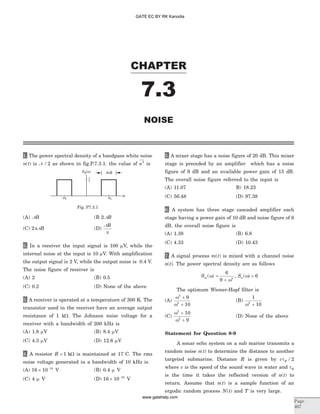
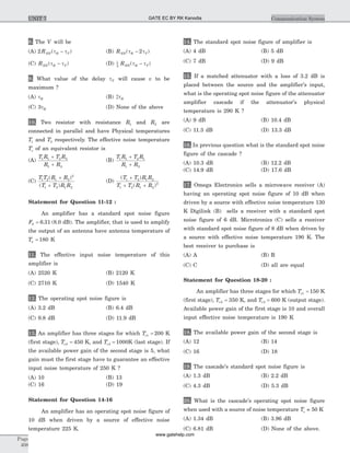
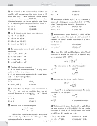
![Statement for Question 44-46 :
An amplifier has a narrow bandwidth of 1 kHz and
standard spot noise figure of 3.8 at its frequency of
operation. The amplifier's available output noise power
is 0.1 mW when its input is connected to a radio
receiving antenna having an antenna temperature of 80
K.
44. The amplifier's input effective noise temperature Te
is
(A) 812 K (B) 600 K
(C) 421 K (D) 321 K
45. Its operating spot noise figure Fop is
(A) 5.16 (B) 7.98
(C) 11.15 (D) 16.23
46. Its available power gain Ga is
(A) 2 1012
´ (B) 4 1012
´
(C) 8 1012
´ (D) 11 1012
´
SOLUTION
1. (B) n2
= =
+
+
ò2
2
2
N
Ndf B
f B
f B
c
c
2. (A) NF = = =
S/N
S/N
/
/
i i
o o
100 10
2 0 4
2
.
3. (A) vn
2
= 4kTBR
= ´ ´ ´ ´ ´ ´-
4 1 38 10 300 200 10 1023 3 3
. = ´ -
3 3 10 12
.
vnrms = 1 8. m V
4. (B) vn
2
= 4kTBR, T K= + =( )273 17 290 K,
R = =1000 104
W, B Hz, k = ´ -
1 38 10 23
. J/K
vn
2
= ´ ´ ´ ´ ´-
4 1 38 10 290 10 1023 3 4
. = ´ -
16 10 14
V 2
vnrms = 0 4. m V
5. (A) F1 = 9 dB = 7.94, F2= 20 dB = 100
A1 = 15 dB = 31.62,
F = +
-
= +
-
=F
F
A
1
2 1
7 94
100 1
31 62
1107.
.
.
6. (C) Gain of each stage A A A1 2 3 10= = = dB
Noise figure of each stage
F F F1 2 3= = = 6 dB or F F F1 2 3= = = 4 db
F = +
-
+
-
F
F
A
F
A A
1
2
1
3
1 2
1 1
= +
-
+
-
=4
4 1
10
4 1
100
4 33.
7. (B) Hop( )w =
S
S S
m
m m
( )
( (
w
w) + w)
=
+
=
+
+
+
6
9
6
9
2
2
2
6
1
10
w
w
w
8. (C) V = - -
-
ò
1
2T
n t n t dtT
T
T
R( ) ( )t t
Since T is very large
V = - -
®¥
-
òlim ( ) ( )
T
T
T
T
R
T
n t n t dt
1
2
t t = - -A n t n tT R[ ( ) ( )]t t
Since N t( ) is ergodic, V » -RNN R T( )t t
9. (A) Because R RNN NN( ) ( )t £ 0 for any auto correlation
function, V will be maximum if t tR T=
10. (B) Use the current form of equivalent circuit
in
2
= + = +i i
kT d
R
kT d
R
1
2
2
2 1
1
2
2
2 2w
p
w
p
where in
2
=
2kT d
R
s w
p
,
Thus Ts = +
æ
è
çç
ö
ø
÷÷
T
R
T
R
R1
1
2
2
=
+
+
T R T R
R R
1 2 2 1
1 2
Chap 7.3
Page
411
Noise GATE EC BY RK Kanodia
www.gatehelp.com](https://image.slidesharecdn.com/a-150815031147-lva1-app6892/85/A-gate-by-rk-kanodia-269-320.jpg)
![11. (D) Te = -T F0 0 1( ) = - =290 6 31 1 1539 9( . ) . K
12. (C) Fop = +1
T
T
e
a
= +1
1540
180
= 9 56. or 9.8 dB
13. (B) Te = = + +250 1
2
1
3
2
T
T
G
T
G
e
e e
250 = + +200
450 1000
51 2G G
or G1 13=
14. (D) F0 = + -1 1
0
T
T
Fs
op( ) = + -1
225
290
10 1( )
= 7 98. or 9.0 dB
15. (D) Here L = 2 089. or 3.2 dB, TL = 290 K
Te= +T
T
G
e
e
1
2
1
= - +
-
T L
T F
L
L ( )
( )
/
1
1
1
0 0
= - + -290 2 089 1 2 089 7 98 1[( . ) ( . )( . )] = 4544 4. K
Fop= + =1
4544 4
225
212
.
. or 13.3 dB
16. (B) F0 = +1
4544 4
290
.
= 16 67. or 12.2 dB
17. (B) For A: Fop = 10(or 10 dB) when Ts = 130 K
TeA = - =130 10 1 1170( ) K
For B: Fo = 398. (or 6 dB) when Ts = 290 K
TeB = - =290 398 1 364 2( . ) . K
For C: Fo = 6 3. (or 8 dB) when Ts = 190 K
TeC = - =190 6 3 1 1007( . ) K, (B) is better as TeB is less.
18. (A) Te = + +T
T
G
T
G G
e
e e
1
1
1
3
1 2
G2 =
- -
T
G T T
e
e e
T
G
e
3
1 1
2
1
( )
=
- -
600
10 190 150 350
10
( )
= 12
19. (B) F0 = +1
0
T
T
e
= +1
190
290
= 1 655. or 2.19 dB
20. (C) Fop = +1
T
T
e
s
= +1
190
50
= 4 8. or 6.81 dB
21. (A) Te = + +T
T
G
T
G G
e
e e
1
2
1
3
1 2
= + + =40
100
8
280
8 6
58 33
( )
. K
22. (B) Te = + +T
T
G
T
G G
e
e e
1
2
1
3
1 2
= + +
é
ëê
ù
ûúT
G G
e1 2
1
1 1
or ( )T T G T G Te e e e1
2
1 1- + + = 0
( )125 155 125 1252
- + +G G = 0
6 25 252
G G- - = 0 or G = 5
23. (A) Sequence Te
ABC110
120
4
150
4 6
146 25+ + =
( )
.
ACB110
150
4
120
4 12
150 00+ + =
( )
.
BAC 120
110
6
150
6 4
144 583+ + = ¬
( )
. Best
CBA150
120
12
110
12 6
161528+ + =
( )( )
.
24. (A) Te = - £ -T F0 1 290 17 1( ) ( . ) = 203 K
25. (D) Here F0 » 1585. (or 2.0 dB) and FOP » 4 467. (or
6.5 dB)
Ts =
-
-
=
-
-
T F
Fop
0 0 1
1
290 1585 1
4 467 1
( ) ( . )
.
= 48 93. K
26. (B) Here Ta = 60 K, L = 1738. (or 2.4 dB), TL = 275 K
and Tsys = 820 K. We know that
TR =
- - -[ ( )]T T T L
L
sys a L 1
=
- - -820 60 275 1738 1
1738
( . )
.
= 320 5. K
27. (B) Fop = +1
T
T
e
s
= +
-
1
T T
T
sys a
s
= +
-
1
820 60
60
= 13 67. or 11.4 dB
28. (A) Here GR( )w0 = 1011
(or 110 dB)
and WPV = 2 107
p( ) Hz
Nclo =
kT G W
L
sys R n( )w
p2
=
-
1 38 10 820 10 10
1738
23 11 7
. ( )( )( )( )
.
= -
651110 5
. or 6.51 mW
29. (C) dNao = + -k T T L
d
a L[ ( )]1
2
w
p
= kT
d
s
w
p2
Thus Ts = + -T T La L ( )1
= + -60 275 1738 1( . ) = 263 K
30. (D) Te = -T Fs op( )1 = -60 5 1( ) = 240 K
31. (C) Fo = +1
290
Te
= +1
240
290
= 1 8276.
32. (A) Fop = +1
T
T
e
s
= + =1
240
30
9 or 9.54 dB
Page
412
Communication SystemUNIT 7 GATE EC BY RK Kanodia
www.gatehelp.com](https://image.slidesharecdn.com/a-150815031147-lva1-app6892/85/A-gate-by-rk-kanodia-270-320.jpg)
![Statement for Question 1 - 3
An AM signal is represented by
x t t t( ) ( sin )cos( )= + ´20 4 500 2 105
p p V
1. The modulation index is
(A) 20 (B) 4
(C) 0.2 (D) 10
2. The total signal power is
(A) 208 W (B) 204 W
(C) 408 W (D) 416 W
3. The total sideband power is
(A) 4 W (B) 8 W
(C) 16 W (D) 2 W
Statement for Question 4 - 5 :
An AM signal has the form
x t t t f tc( ) [ cos cos ]cos= + +20 2 3000 10 6000 2p p p where
fc = 105
Hz.
4. The modulation index is
(A) 201
400
(B) - 201
400
(C) 199
400
(D) - 199
400
5. The ratio of the sidebands power to the total power is
(A) 43
226
(B) 26
226
(C) 26
226
(D) 43
224
6. A 2 kW carrier is to be modulated to a 90% level. The
total transmitted power would be
(A) 3.62 kW (B) 2.81 kW
(C) 1.4 kW (D) None of the above
7. An AM broadcast station operates at its maximum
allowed total output of 50 kW with 80% modulation.
The power in the intelligence part is
(A) 12.12 kW (B) 31.12 kW
(C) 6.42 kW (D) None of the above
8. The aerial current of an AM transmitter is 18 A when
unmodulated but increases to 20 A when
modulated.The modulation index is
(A) 0.68 (B) 0.73
(C) 0.89 (D) None fo the above
9. A modulating signal is amplified by a 80% efficiency
amplifier before being combined with a 20 kW carrier to
generate an AM signal. The required DC input power to
the amplifier, for the system to operate at 100%
modulation, would be
(A) 5 kW (B) 8.46 kW
(C) 12.5 kW (D) 6.25 kW
10. A 2 MHz carrier is amplitude modulated by a 500
Hz modulating signal to a depth of 70%. If the
unmodulated carrier power is 2 kW, the power of the
modulated signal is
(A) 2.23 kW (B) 2.36 kW
(C) 1.18 kW (D) 1.26 kW
11. A carrier is simultaneously modulated by two sine
waves with modulation indices of 0.4 and 0.3. The
resultant modulation index will be
(A) 1.0 (B) 0.7
(C) 0.5 (D) 0.35
CHAPTER
7.4
AMPLITUDE MODULATION
Page
414
GATE EC BY RK Kanodia
www.gatehelp.com](https://image.slidesharecdn.com/a-150815031147-lva1-app6892/85/A-gate-by-rk-kanodia-271-320.jpg)
![12. In a DSB-SC system with 100% modulation, the
power saving is
(A) 50% (B) 66%
(C) 75% (D) 100%
13. A 10 kW carrier is sinusoidally modulated by two
carriers corresponding to a modulation index of 30%
and 40% respectively. The total radiated power(is
(A) 11.25 kW (B) 12.5 kW
(C) 15 kW (D) 17 kW
14. In amplitude modulation, the modulation envelope
has a peak value which is double the unmodulated carrier
value. What is the value of the modulation index ?
(A) 25% (B) 50%
(C) 75% (D) 100%
15. If the modulation index of an AM wave is changed
from 0 to 1, the transmitted power
(A) increases by 50% (B) increases by 75%
(C) increases by 100% (D) remains unaffected
16. A diode detector has a load of 1 kW shunted by a
10000 pF capacitor. The diode has a forward resistance
of 1 W. The maximum permissible depth of modulation,
so as to avoid diagonal clipping, with modulating signal
frequency fo 10 kHz will be
(A) 0.847 (B) 0.628
(C) 0.734 (D) None of the above
17. An AM signal is detected using an envelop detector.
The carrier frequency and modulating signal frequency
are 1 MHz and 2 kHz respectively. An appropriate value
for the time constant of the envelope detector is.
(A) 500 m sec (B) 20 m sec
(C) 0.2 m sec (D) 1 m sec
18. An AM voltage signal s t( ), with a carrier frequency
of 1.15 GHz has a complex envelope g t A m tC( ) [ ( )],= +1
where Ac = 500 V, and the modulation is a 1 kHz
sinusoidal test tone described by m t t( ) . sin( )= ´0 8 2 103
p
appears across a 50 W resistive load. What is the actual
power dissipated in the load ?
(A) 165 kW (B) 82.5 kW
(C) 3.3 kW (D) 6.6 kW
19. A 1 MHz sinusoidal carrier is amplitude modulated
by a symmetrical square wave of period 100 m sec.
Which of the following frequencies will NOT be present
in the modulated signal?
(A) 990 KHz (B) 1010 KHz
(C) 1020 KHz (D) 1030 KHz
20. For an AM signal, the bandwidth is 10 kHz and the
highest frequency component present is 705 kHz. The
carrier frequency used for this AM signal is
(A) 695 kHz (B) 700 kHz
(C) 705 kHz (D) 710 kHz
21. A message signal m t t t( ) ( )= +sinc sinc2
modulates
the carrier signal ( ) cost A f tc= 2p . The bandwidth of the
modulated signal is
(A) 2 fc (B) 1
2
fc
(C) 2 (D) 1
4
22. The signal m t t t( ) cos cos= +2000 2 4000p is
multiplied by the carrier c t f tc( ) cos= 100 2p where fc = 1
MHz to produce the DSB signal. The expression for the
upper side band (USB) signal is
(A) 100 2 1000 200 2 200cos( ( ) ) cos( ( ) )p pf t f tc c+ + +
(B) 100 2 1000 200 2 2000cos( ( ) ) cos( ( ) )p pf t f tc c- + -
(C) 50 2 1000 100 2 2000cos( ( ) ) cos( ( ) )p pf t f tc c+ + +
(D) 50 2 1000 100 2 100cos( ( ) ) cos( ( ) )p pf t f tc c- + -
Statement for Question 23-26 :
The Fourier transform M f( ) of a signal m t( ) is
shown in figure. It is to be transmitted from a source to
destination. It is known that the signal is normalized,
meaning that - £ £1 1m t( )
23. If USSB is employed, the bandwidth of the
modulated signal is
(A) 5 kHz (B) 20 kHz, 10 kHz
(C) 20 kHz (D) None of the above
24. If DSB is employed, the bandwidth of the modulated
signal is
(A) 5 kHz (B) 10 kHz
(C) 20 kHz (D) None of the above
Chap 7.4
Page
415
Amplitude Modulation
M f( )
f
10000-10000
Fig.P7.4.23-26
GATE EC BY RK Kanodia
www.gatehelp.com](https://image.slidesharecdn.com/a-150815031147-lva1-app6892/85/A-gate-by-rk-kanodia-272-320.jpg)
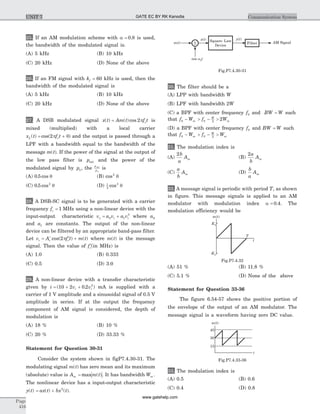
![34. The modulation efficiency is
(A) 8.3 % (B) 14.28 %
(C) 7.69 % (D) None of the above
35. The carrier power is
(A) 60 W (B) 450 W
(C) 30 W (D) 900 W
36. The power in sidebands is
(A) 85 W (B) 42.5 W
(C) 56 W (D) 37.5 W
37. In a broadcast transmitter, the RF output is
represented as
e t t t t( ) [ . cos . sin ]cos( )= + + ´50 1 0 89 5000 0 30 9000 6 106
V
What are the sidebands of the signals in radians ?
(A) 5 10 9 103 3
´ ´and
(B) 5 991 10 5 995 10 6 005 10 6 009 106 6 6 6
. , . , . .´ ´ ´ ´and
(C) 4 10 1 4 103 4
´ ´, .
(D) 1 10 11 10 3 10 15 106 7 6 7
´ ´ ´ ´, . , , .and
38. An AM modulator has output
x t t t t( ) cos cos cos= + +40 400 4 360 4 440p p p
The modulation efficiency is
(A) 0.01 (B) 0.02
(C) 0.03 (D) 0.04
39. An AM modulator has output
x t A t B t B t( ) cos cos cos= + +400 380 420p p p
The carrier power is 100 W and the efficiency is
40%. The value of A and B are
(A) 14.14, 8.16 (B) 50, 10
(C) 22.36, 13.46 (D) None of the above
Statement for Question 40-41
A single side band signal is generated by
modulating signal of 900-kHz carrier by the signal
m t t t( ) cos sin= +200 2 2000p p . The amplitude of the
carrier is Ac = 100.
40. The signal $ ( )m t is
(A) - -sin( ) cos( )2 1000 2 2000p pt t
(B) - +sin( ) cos( )2 1000 2 2000p pt t
(C) sin( ) cos( )2 1000 2 1000p t t+
(D) sin( ) cos( )2 1000 2 2 1000p pt t-
41. The lower sideband of the SSB AM signal is
(A) - - + -100 2 1000 200 2 1000cos( ( ) ) sin( ( ) )p pf t f tc c
(B) - - - -100 2 1000 200 2 1000cos( ( ) ) sin( ( ) )p pf t f tc c
(C) 100 2 1000 200 2 1000cos( ( ) ) sin( ( ) )p pf t f tc c- - -
(D) 100 2 1000 200 2 1000cos( ( ) ) sin( ( ) )p pf t f tc c- + -
Statement for Question 42-43
Consider the system shown in figure 6.69-70. The
average value of m t( ) is zero and maximum value of
m t( ) is M. The square-law device is defined by
y t x t x t( ) ( ) ( )= +4 10 .
42. The value of M, required to produce modulation
index of 0.8, is
(A) 0.32 (B) 0.26
(C) 0.52 (D) 0.16
43. Let W be the bandwidth of message signal m t( ). AM
signal would be recovered if
(A) f Wc > (B) f Wc > 2
(C) f Wc ³ 3 (D) f Wc > 4
44. A super heterodyne receiver is designed to receive
transmitted signals between 5 and 10 MHz. High-side
tuning is to be used. The tuning range of the local
oscillator for IF frequency 500 kHz would be
(A) 4.5 MHz - 9.5 MHz
(B) 5.5 MHz - 10.5 MHz
(C) 4.5 MHz - 10.5 MHz
(D) None of the above
45. A super heterodyne receiver uses an IF frequency of
455 kHz. The receiver is tuned to a transmitter having
a carrier frequency of 2400 kHz. High-side tuning is to
be used. The image frequency will be
(A) 2855 kHz (B) 3310 kHz
(C) 1845 kHz (D) 1490 kHz
Chap 7.4
Page
417
Amplitude Modulation
m t( )
cos twc
AM SignalSquare- Law
Device
y t( )x t( )
FilterS
Fig. P7.4.42-43
GATE EC BY RK Kanodia
www.gatehelp.com](https://image.slidesharecdn.com/a-150815031147-lva1-app6892/85/A-gate-by-rk-kanodia-274-320.jpg)
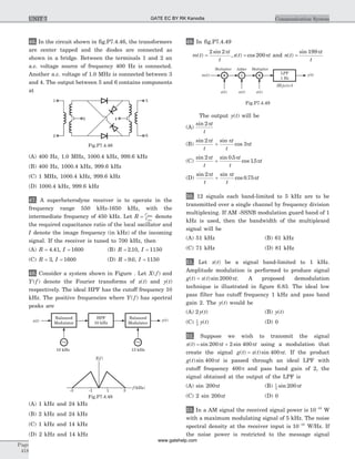
![bandwidth only, the signals-to-noise ratio at the input
to the receiver is
(A) 43 dB (B) 66 dB
(C) 56 dB (D) 33 dB
Statement for Question 54-55
Consider the following Amplitude Modulated (AM)
signal, where f Bm <
x t f t f tAM m c( ) ( . sin )cos= +10 1 0 5 2 2p p .
54. The average side-band power for the AM signal
given above is
(A) 25 (B) 12.5
(C) 6.25 (D) 3.125
55. The AM signal gets added to a noise with Power
Spectra Density S fn ( ) given in the figure below. The
ration of average sideband power to mean noise power
would be
(A)
25
8 0N B
(B)
25
4 0N B
(C)
25
2 0N B
(D)
25
0N B
Statement for Question 56-57
A certain communication channel is characterized
by 80 dB attenuation and noise power-spectral density
of 10 10-
W/Hz. The transmitter power is 40 kW and the
message signal has a bandwidth of 10 kHz.
56. In the case of conventional AM modulation, the
predetecion SNR is
(A) 108
(B) 2 108
´
(C) 102
(D) 2 102
´
57. In case of SSB, the predetecion SNR is
(A) 2 102
´ (B) 4 102
´
(C) 2 103
´ (D) 4 103
´
*************
SOLUTION
1. (C) u t( ) = + ´( sin )cos( )20 4 500 2 105
p pt t V
= + ´20 1 0 2 500 2 105
( . sin )cos( )p pt t V, a = 0 2.
2. (B) Pc =
20
2
2
= 200 W, Pt = +
æ
è
çç
ö
ø
÷÷Pc 1
0 2
2
2
( . )
= 204 W
3. (A) Psb = -P Pt c = -204 200 = 4 W
4. (B) x t( )
= + +[ cos( ) cos( )]cos( )20 2 2 1500 10 2 3000 2p p pt t f tc
= + +
æ
è
ç
ö
ø
20 1
1
10
2
1
2
2 3000 2cos( ) cos( )cos( )p1500 p pt t f tc ÷
This is the form of a conventional AM signal with
message signal
m t( ) = +
1
10
2 1500
1
2
2 3000cos( ) cos( )p pt t
= + -cos ( ) cos( )2
2 1500
1
10
2 1500
1
2
p pt t
The minimum of g z z z( ) = + -2 1
10
1
2
is achieved for
z = -
1
20
and it is min( ( ))g z = -
201
400
. Since z = -
1
20
is in
the range of cos ( )2 1500p t , we conclude that the
minimum value of m t( ) is -
201
400
. Hence, the modulation
index is a = -
201
400
5. (B) x t( ) = + -20 2 2 1500cos( ) cos( ) )p p(f t f tc c
+ -cos( ) )2 1500p(f tc
= + +5 2 3000 5 2 3000cos( ) ) cos( ) )p( p(f t f tc c
The power in the sidebands is
Psidebands = + + + =
1
2
1
2
25
2
25
2
26
The total power is P P Ptotal carrier sidebands= + = + =200 26 226
The ratio of the sidebands power to the total power is
P
P
sidebands
total
=
26
226
6. (B) Pt = +
æ
è
çç
ö
ø
÷÷Pc 1
2
2
a
= +
æ
è
çç
ö
ø
÷÷2000 1
0 9
2
2
.
= 2810 W
7. (A) Pt = +
æ
è
çç
ö
ø
÷÷Pc 1
2
2
a
or 50 103
´ = +
æ
è
çç
ö
ø
÷÷Pc 1
0 8
2
2
.
Pc = 37 88. kW, Pi = - = - =( ) ( . ) .P Pt c 50 37 88 12 12 kW
Chap 7.4
Page
419
Amplitude Modulation GATE EC BY RK Kanodia
www.gatehelp.com](https://image.slidesharecdn.com/a-150815031147-lva1-app6892/85/A-gate-by-rk-kanodia-276-320.jpg)
![8. (A) It = +
æ
è
çç
ö
ø
÷÷Ic 1
2
2
1
2a
or 20 = +
æ
è
çç
ö
ø
÷÷18 1
2
2
1
2a
or a = 0 68.
9. (C) Pt = +
æ
è
ç
ö
ø
÷20000 1
1
2
, Pt = 30 kW,
Pi = - =30 20 10 kW
The DC input power = =
10
0 8
12 5
.
. kW.
10. (A) Pc= 2 kW, a = =70 0 7% .
Pt = +
æ
è
çç
ö
ø
÷÷Pc 1
2
2
1
2a
= +
æ
è
çç
ö
ø
÷÷ =2 1
0 7
2
2 23
2
.
. kW
11. (C) a2
= +a a1 2
2a
= +0 3 0 42 2
. . = 0 52
. or a = 0 5.
12. (B) In previous solution Pc=
2
3
P. If carrier is
suppressed then
2
3
P or 66% power will be saved.
13. (A) Pt = + +
æ
è
çç
ö
ø
÷÷Pc 1
2 2
1
2
2
2
a a
= + +
æ
è
çç
ö
ø
÷÷10 1
0 3
2
0 4
2
2 2
. .
= 1125. kW
14. (D) x t( ) = +A f t f tc m c( cos )cos1 2 2a p p
Here Ac( )1 + a = 2 Ac, Thus a =1, therefor modulation
index is 1 or 100% modulation.
15. (A) If modulation index a is 0, then
Pt1 = +
æ
è
çç
ö
ø
÷÷
Ac
2 2
2
1
0
2
=
Ac
2
2
If modulation index is 1 then
Pt2 = +
æ
è
çç
ö
ø
÷÷
Ac
2 2
2
1
1
2
=
3
4
2
Ac ,
P
P
t
t
2
1
3
2
=
Thus Pt2 = 15 1. Pt and Pt2 is increases by 50%
16. (A) fm = 10 kHz, R = 1000 W, C = 10000 pF
Hence 2pf RCm = ´ ´ ´ =-
2 10 10 10 0 6284 3 8
p .
amax = + =
-
( ( . ) ) .1 0 628 0 8472
1
2
17. (B)
1 1
f
RC
BWc m
£ £ , Here fc = 1 MHz
Signal Bandwidth BWm = 2 fm = ´ ´ =2 2 10 43
kHz
Thus
1
106
£ £
´
RC
1
4 103
or 10 6-
£ RC £ 250 ms
Thus appropriate value is 20 m sec
18. (A) Pt = +
é
ë
ê
ê
ù
û
ú
ú
A m tc
2 2 2
2
1
2
a ( )
Here modulation index a =1. Thus
Pt = +
é
ë
ê
ù
û
ú
500
2
1
0 8
2
2 2
.
= 165 kW
19. (C) c t( ) = sin 2p f tc , fc = 1000 kHz, x t( ) = c t m t( ) ( )
Expressing square wave as modulating signal m t( )
m t( ) [ ]=
-
-
-
-
=
¥
å
4 1
2 1
2 2 1
1
1p
p
( )
cos ( )
n
n
m
n
f n
The modulated output
x t( ) =
-
-
-
é
ë
ê
ù
û
ú
-
=
¥
å
4 1
2 1
2 2 1 2 1000
1
1p
p p
( )
cos[ ( )] sin(
n
m
n n
f n ´ 103
t)
So frequency component ( ( )10 2 16
± -f nm will be present
where n = 1 2 3, , , ....
For fm = 10 kHz and n = 1 2& frequency present is 990,
970, 1030 kHz. Thus 1020 kHz will be absent.
20. (B) f fc m+ = 705 kHz,
BW = =2 10fm kHz or fm = 5 kHz
fc = - =705 5 700 kHz
21. (C) x t( ) = m t c t( ) ( ) = +A t t f tc( ( ) ( )cos( )sinc sinc2
2p
Taking the Fourier transform of both sides, we obtain
X f( ) = + - + +
A
f f f f f fc c
2
[ ( ) ( )]* ( ( ) ( ))P L d d
= - + - + + + -
A
f f f f f f f fc c c c
2
[ ( ) ( ) ( ) ( )]P L P L
Since P( )f fc- ¹ 0 for f fc- <
1
2
, whereas L( )f fc- ¹ 0
for f fc- < 1. Hence, the bandwidth of the bandpass
filter is 2.
22. (C) x t( ) = m t c t( ) ( )
= +100 2 000 2 2 2000 2[cos( ) cos( )]cos( )p1 p pt t f tc
= +100 2 000 2 200 2 2cos( )cos( ) cos( )cos(p1 p p2000 pt f t t fc ct)
= + + -
100
2
2 000 2 1000[cos( ( ) ) cos( ( ) )]p 1 pf t f tc c
+ + + -
200
2
2 2000 2 2000[cos( ( ) ) cos( ( ) )]p pf t f tc c
Thus, the upper sideband (USB) signal is
x tu( ) = + + +50 2 000 100 2 2000cos[ ( ) ] ( ( ) )p 1 pf t f tc c
23. (B) When USSB is employed the bandwidth of the
modulated signal is the same with the bandwidth of the
message signal. Hence W WUSSB = = 104
Hz
Page
420
Communication SystemUNIT 7 GATE EC BY RK Kanodia
www.gatehelp.com](https://image.slidesharecdn.com/a-150815031147-lva1-app6892/85/A-gate-by-rk-kanodia-277-320.jpg)
![37. (B) Sidebands are ( )6 10 50006
´ ± and
( )6 10 90006
´ ±
Thus 6 005 10 5 995 10 5 991 106 6 6
. , . , .´ ´ ´ or 5 991 106
. ´ ,
6 005 106
. ´ and 6 009 106
. ´
38. (B) x t( ) can be written as
x t( ) = +( cos )cos40 8 40 400p pt t
modulation index a = =
8
40
0 2.
Pc =
1
2
40 2
( ) = 800 W
The components at 180 Hz and 220 Hz are side band
Psb = +
1
2
4
1
2
42 2
( ) ( ) = 16 W,
Eeff =
+
P
P P
sb
c sb
=
+
16
800 16
39. (A) Carrier power Pc= =
A2
2
100 W, A = 14 14.
Eeff =
+
=
P
P P
sb
c sb
40
100
or
P
P
sb
sb100 +
= 0 4.
Psb = 66 67. W, Psb = + =
1
2
1
2
66 672 2
B B . or B = 8 161.
40. (D) The Hilbert transform of cos ( )2 1000p t is
sin ( )2 1000p t , whereas the Hilbert transform of
sin ( )2 1000p t is cos ( )2 1000p t
Thus $ ( )m t = -sin ( ) cos ( )2 1000 2 1000p pt t
41. (D) The expression for the LSSB AM signal is.
x tl
( ) = +A m t f t A m t f tc c c c( )cos( ) ( )sin( )2 2p p
Substituting
Ac = = +100 2 1000 2 2 1000, ( ) cos( ) sin( )m t t tp p
and $ ( )m t = -sin( ) cos( )2 1000 2 2 1000p pt t
we obtain
x tl( ) = +100 2 1000 2 2 1000 2[cos( ) sin( )cos( )]p p pt t f tc
+ -100 2 1000 2 2 1000 2[sin( ) cos( )sin( )]p p pt t f tc
= +100 2 1000 2 2 1000 2[cos( )cos( ) sin( )sin( )p p p pt f t t f tc c ]
+ -200 2 2 1000 2 2 1000[cos( )sin( ) sin( )cos( )p p p pf t t f t tc c ]
= - - -100 2 1000 200 2 1000cos( ( ) ) sin( ( ) )p pf t f tc c
42. (D) y t( ) = + + +4 10 2
( ( ) cos ) ( ( ) cos )m t t m t tc cw w
= + + + + +4 4 10 20 5 5 22
m t t m t m t t tc c c( ) cos ( ) ( ) cos cosw w w
= + + + + +5 4 10 4 1 5 5 22
m t m t m t t tc c( ) ( ) [ ( )] cos cosw w
The AM signal is, x tc( ) = +4 1 5[ ( )]cosm t tcw
m t( ) = Mm tn ( )
x tc( ) = +4 1 5[ ( )]cosMm t tn cw
5M = 0 8. or M = 0 16.
43. (C) The filter characteristic is shown in fig.S7.4.43
f W Wc - > 2 or f Wc > 3 ,
f W fc + < 2 or f Wc >
Therefore f Wc > 3
44. (B) Since High-side tuning is used
fLO = + =f fm IF 500 kHz,
fLOL = + =5 0 5 5 5. . MHz,
fLOU = + =10 0 5 10 5. . MHz
45. (B) fimage = + = =f fL IF2 2400 3310 kHz
46. (D) The given circuit is a ring modulator. The output
is DSB-SC signal. So it will contain m t n tc( )cos( )w where
n = 1 2 3, , ...... Therefore there will be only (1 MHz ± 400
Hz) frequency component.
47. (A) fmax = + =1650 450 2100 kHz
fmin = + =550 450 1000 kHz. or f =
1
2p LC
frequency is minimum, capacitance will be maximum
R = = =
C
C
f
f
max
min
max
min
( . )
2
2
2
2 1 or R = 4 41.
fi = +f fc IF2 = +700 2 455( ) = 1600 kHz
48. (B) Since X f( ) has spectral peak at 1 kHz so at the
output of first modulator spectral peak will be at ( )10 1+
kHz and ( )10 1- kHz. After passing the HPF frequency
component of 11 kHz will remain. The output of 2nd
modulator will be ( )13 11± kHz. So Y f( ) has spectral
peak at 2 kHz and 24 kHz.
49. (C) m t s t y t( ) ( ) ( )= 1
=
2 2 200sin( )cos( )p pt t
t
=
-sin( ) sin( )202 198p pt t
t
y t n t1( ) ( )+ = y t2( ) =
-
+
sin sin sin202 198 198p p pt t
t
t
t
y t s t2( ) ( ) = y t( )
=
- +[sin sin sin ]cos202 198 199 200p p p pt t t t
t
Page
422
Communication SystemUNIT 7
f
2WW 2fcfc fc+Wfc-W
H f( )
m t( )
Fig.S7.4.43
GATE EC BY RK Kanodia
www.gatehelp.com](https://image.slidesharecdn.com/a-150815031147-lva1-app6892/85/A-gate-by-rk-kanodia-278-320.jpg)
![= + - -
1
2
402 2 398 2[sin( ) sin( ) {sin( ) sin( )}p p p pt t t t
+ -sin( ) sin( )]399p pt t
After filtering
y t( ) =
+ -sin( ) sin( ) sin( )2 2
2
p p pt t t
t
=
+sin( ) sin( . )cos( . )2 2 0 5 15
2
p pt t t
t
= +
sin sin .
cos .
2
2
0 5
15
p p
p
t
t
t
t
t
50. (D) The total signal bandwidth = 5 12 60´ = kHz
There would be 11 guard band between 12 signal. So
guard band width = 11 kHz
Total band width = 60 + 11 = 71 kHz
51. (D) x t1( ) = g t t( )cos( )2000p
= x t t t( )sin( )cos( )2000 2000p p =
1
2
4000x t t( )sin( )p
X j1( )w = - - +
1
4
4000 4000
j
X j X j( ( )) ( ( ))w p w p
This implies that X j1( )w is zero for w p£ 2000 because
w p p< =2 2 1000fm . When x t1( ) is passed through a LPF
with cutoff frequency 2000p, the output will be zero.
52. (A) y t( ) = =g t t x t t( )sin( ) ( )sin ( )400 4002
p p
= +
-
(sin( ) sin( )
( cos)( )
200 2 400
1 800
2
p p
p
t t
t
= - +
1
2
200 200 800 2 400[sin( ) sin( )cos( ) sin( )p p p pt t t t
-sin( )cos( )400 800p pt t
= - -
1
2
200
1
4
1000 6000sin( ) [sin( ) sin( )]p p pt t t
+ - -sin( ) [sin( ) sin( )]400
1
4
1200 400p p pt t t
If this signal is passed through LPF with frequency
400p and gain 2, the output will be sin( )200pt
53. (A) Message signal BW fm = 5 kHz
Noise power density is 10 18-
W/Hz
Total noise power is 10 5 10 5 1018 3 15- -
´ ´ = ´ W
Input signal-to-noise ratio
SNR=
´
= ´
-
-
10
5 10
2 10
10
15
4
or 43 dB
54. (C) Average side band power is
Ac
2 2
4
a
=
10 0 5
4
2 2
( . )
= 6 25. W
55. (D) Noise power = Area rendered by the spectrum
= N B0
Ratio of average sideband power to mean noise
Power = =
6 25 25
40 0
.
N B N B
56. (C) Since the channel attenuation is 80 db, then
10 log
P
P
T
R
= 80
or P PR T= -
10 8
= ´ ´ = ´- -
10 40 10 4 108 3 4
Watts
If the noise limiting filter has bandwidth B, then the
pre-detection noise power is
Pn = 2
2
2 100
0
10
2
2
N
df N B
f
B
f
B
c
c
= = ´ -
-
+
ò B Watts
In the case of DSB or conventional AM modulation,
B W= = ´2 2 104
Hz, whereas in SSB modulation
B W= = 104
. Thus, the pre-detection signal to noise
ratio in DSB and conventional AM is
SNRDSB,AM = =
´
´ ´ ´
=
-
-
P
P
R
n
4 10
2 10 2 10
10
4
10 4
2
57. (A) In SSB modulation B = W = 104
SNRSSB =
´
´ ´
= ´
-
-
4 10
2 10 10
2 10
4
10 4
2
***********
Chap 7.4
Page
423
Amplitude Modulation GATE EC BY RK Kanodia
www.gatehelp.com](https://image.slidesharecdn.com/a-150815031147-lva1-app6892/85/A-gate-by-rk-kanodia-279-320.jpg)
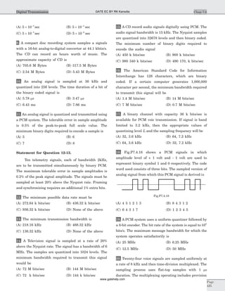


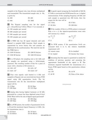
![16. (C) 128= 27
,. We need 7 bits/character. For 1,000,000
character we need 7 Mbits/second. Thus minimum
bandwidth = 7 Mbits/sec.
17. (D) f fs m> 2 = 6400 Hz, nfs £ 63000
n £ =
36000
6400
5 63. , n = 5, L n
= 2 = 32, fs = =
36000
5
7 2. kHz.
18. (D) The transmitted code word are
In 1st word 001(1)
In 2nd word 010(2)
In 3rd word 011(3)
In 4th word 100(4)
In 5th word 101 (5)
19. (B) Message bandwidth= W, Nyquist rate = 2W
Bandwidth = ´2 8W = 16W bit/s
16W= 108
, or W = =
10
16
6 25
8
. MHz
20. (A) Sampling interval T
k
, = =
1
8
125 ms. There are 24
channels and 1 sync pulse, so the time allotted to each
channel is Tc
T
= =25
5 ms. The pulse duration is 1 ms. So
the time between pulse is 4 ms.
21. (B) Amax= =
´
´
d
w p
f ks
m
0 1 68
2 103
.
= 108. V
22. (D) Amax =
d
w
fs
m
or d =
A
f
m
s
maxw
=
´ ´
´
1 2 800
50 103
p
= 78.5 mV
23. (D) No =
d2
3
B
fs
=
´
´
( . )0 0785 3500
3 64000
2
= ´ -
1122 10 4
. W
24. (C)
S
N
o
o
=
´ -
0 5
112 10 4
.
.
= ´4 46 103
.
25. (A)
S
N
Lo
o
µ 2
, L =
æ
è
çç
ö
ø
÷÷2n o
o dB
S
N
= 10 22
log( )C n
= + = +log logC n n20 2 6a dB. This equation shows
that increasing n by one bits increase the by 6 dB.
Hence an increase in the SNR by 12 dB can be
accomplished by increasing 9is form 10 to 12, the
transmission bandwidth would be increased by 20%
26. (B)
S
N
o
o
=
+
3
1
2
2
L
[ln( )]m
= 6394 = 38 06. dB
27. (C) Nyquist Rate = 2 MHz
50% higher rate = 3 MHz, L = =256 28
Thus transmission bandwidth is 3 MHz ´ =8 24 Mbits/s.
New sampling rate is at 20% above the Nyquist rate.
Sampling rate= ´ =12 2 2 4. . MHz.
bits per second=
24
2 4
M
MHz
bits
sec
.
= 10 bits
Level = =2 102410
,
S
N
o
o
= = =
3 1024
256
102300 50 1
2
2
( )
(ln )
. dB
28. (B)
S
N
o
o
=
+
³
3
1
50
2
2
L
[ln( )]m
dB, m = 100
3
101
2
2
L
[ln )
= 100 000 or L = 842 6.
Because L is power of 2, we select L = =1024 210
.
Thus 10 bits are required.
29. (A) So = =m t N
m
L
o
p2
2
2
3
3
( ), ,
S
N
o
o
=
3 2 2
2
L m t
mp
( )
since signal is sinusoidal
m t
mp
2
2
1
2
( )
= ,
3
2
48
2
L
= dB = 63096, L = 205 09.
Since L is power of 2, so we select L = 256
Hence 256 = 28
, So 8 bits per sample is required .
30. (B) ( ) . . ( ) , .SNR n dB nq = + = =176 6 02 40 6 35
We take the n = 7.
Capacity = 20 8 7 112´ ´ =k . Mbits = 140 Kbytes
31. (B) For slope overload to take place E
f
f
m
s
m
³
d
p2
This is satisfied with Em = 15. V and fm = 4 kHz.
32. (C) Step size d= = =
2 1536
128
0 012
m
L
p .
. V
quantization noise power
= =
d2 2
12
0 012
12
( . )
= ´ -
12 10 6 2
V
33. (B) Bit Rate = ´8 8k = 64 kbps
(SNR)q= +176 6 02. . n dB = + ´ =176 6 02 8 49 8. . . dB
34. (B) fs = 1800 samples/sec, fm = =
1800
2
900 Hz
Page
440
Communication SystemUNIT 7
0 0 0 0 0 0 0 01 1 1 1 1 11
Fig.S.7.6.18
GATE EC BY RK Kanodia
www.gatehelp.com](https://image.slidesharecdn.com/a-150815031147-lva1-app6892/85/A-gate-by-rk-kanodia-285-320.jpg)
![Since the sampling rate is 1800 samples/sec the highest
frequency that can be recovered is 900 Hz.
35. (C) x t( ) = sinc 700t + sinc 500t
[ ]= +
1
700 500
p
p p
t
t tsin sin
x t( ) is band limited with fm = 350 Hz, Thus Nyquist
rate is 2 fm = 700 Hz, Sampling interval =
1
700
sec
36. (D) fs= =
´
=-
1 1
50 10
206
T
kHz, fc= 12 kHz
The frequency passed through LPF are f f fc s m, - or 12
kHz, 8 kHz
37. (C) P = =
( )SNR
(SNR)2
1
2
2
2
2
2
1
n
n
, Here n = code word length,
n1 16= n2 8= , Thus rate =
2
2
16
16
12
=
38. (D) Signal g t g t g ts1 2( ), ( ), ( ) and g t4( ) will have 8 k, 8
k, 16 k and 16 k sample/sec at Nyquist rate. Thus
48000 sample/sec bit rate 48000 8 384´ = kbps
39. (C) Analog signals, having bandwidth 1200 Hz, 600
Hz and 600 Hz have 2400, 1200 samples/sec at Nyquist
rate. Hence 48000 sample/sec
bit rate = 48000 sample/sec ´12 = 57 6. kbps
40. (C) x t( ) =
æ
è
ç
ö
ø
÷ +
æ
è
ç
ö
ø
÷5
2 1000
7
2
3 2
sin sinp
p
p1000
p
t
t
t
t
Maximum frequency component = ´ =3 1000 3 kHz
Sampling rate = =2 6fm kHz
41. (B) Here fs = 32 k sample/sec
Em = 125, fm = =
1 1
2T
For slope-overload to be averted Em ³
f
f
s
m
D £
E f
f
m m
s
or D £
´
125
32 10
1
2
3
( )
or D £
´
( )( )128
32 1024
1
2
or D £ -
2 8
42. (D) fm = 5 kHz, Nyquist Rate = ´2 5 = 10 kHz
Since signal are sampled at twice the Nyquist rate so
sampling rate = ´ =2 10 20 kHz.
Total transmission bandwidth = ´ =4 20 80 kHz
43. (D) Signal will be sampled 200, 200, 400 and 800
sample/sec thus 1600 sample per second,
44. (D) g t( ) =
+æ
è
ç
ö
ø
÷10 50
1 300
2
cos
cos
p
p
t
t
= +5 50 5 50 300cos cos cosp p pt t t
The maximum frequency component will be
150 25 175+ = Hz.
Thus fs = ´ =2 175 350. sample per second.
45. (B) Total sample = ´8000 20 = 160 k sample/sec
Bit for each sample = + =7 1 8
Bit Rate = ´160 8k = ´1280 103
bits/sec
46. (B) The sampling rate is fs = 44100 meaning that we
take 44100 samples per second. Each sample is
quantized using 16 bits so the total number of bits per
second is 44100´16. For a music piece of duration 50
min = 3000- sec the resulting number of bits per
channel (left and right) is 44100 16 3000´ ´
= ´2 1168 109
. and the overall number of bits is
2 1168 10 29
. ´ ´ = ´4 2336 109
.
47. (C) Nyquist Rate = ´ =2 4k 8 kHz
Total sample = ´ =4 8 32 k sample/sec
256 = 28
, so that 8 bits are required
Bit Rate = ´32 8k = 256 kbps
48. (D) Nyquist Rate = ´ =2 30 60k kHz
2 6n
³ Thus n = 3, Bit Rate = ´60 3 = 18 kHz
49. (C) Nyquist rate= ´ =2 4 8 kHz
2n
= 16 or n = 4, Bit Rate = ´ =4 8 32 kbits/sec
50. (C) fs = 8 kHz, 2n
= Þ =256 8n
Bit Rate = ´8 8k = 64 kb/x
51. (D)
S
N
o
o
n
a 22
, If PCM is increased form n to n + 1,
the ratio will increase by a factor 4. Which is
independent of n.
52. (C) If L = 2, then 2 2= n
or n = 1 ND If L = 8, then
8 2= n
or n = 3. So relative bandwidth will be tripled.
53. (B) The minimum bandwidth requirement for
transmission of a binary PCM signal is BW= vW. Since
v = 10, we have BW = 10 W
***********
Chap 7.6
Page
441
Digital Transmission GATE EC BY RK Kanodia
www.gatehelp.com](https://image.slidesharecdn.com/a-150815031147-lva1-app6892/85/A-gate-by-rk-kanodia-286-320.jpg)
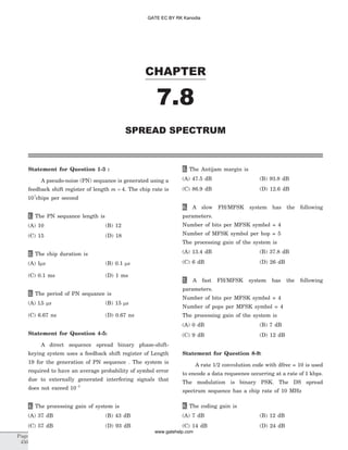
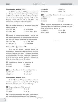
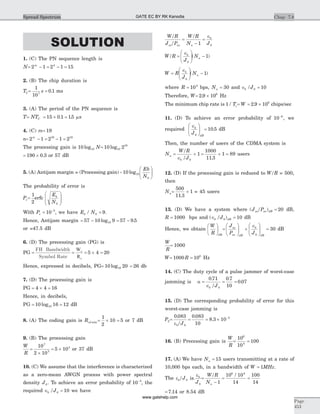

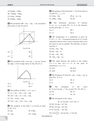
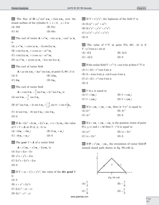
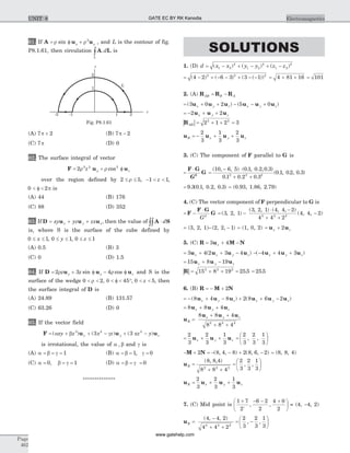
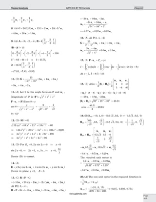
![u AM =
-
+ +
=
( , , )20 18 10
400 324 100
(0.697, 0.627, -0.348)
1
2
( )u uAM AN+
[ ]= - + -
1
2
0 697 0 627 0 348 0 507 0 406 0 761( . , . , . ) ( . , . , . )
= (0.095, 0.516, 0.207)
ubis =
+ +
( . , . , . )
. . .
0 095 0 516 0 207
0 095 0 516 0 2612 2 2
= (0.168, 0.915, 0.367)
Hence (A) is correct.
21. (D) In cartesian coordinates
A ( cos , sin , ) ( . , . , )5 70 5 70 3 171 4 70 3° ° - = -A
B ( cos ( ), sin ( ), ) ( . , , )2 30 2 30 3 173 1 1- ° - ° - = -B
R R RAB B A= - = - - -( . , , ) ( . , . , )173 1 1 171 4 70 3
= -( . , . , )0 02 5 70 4
u AB =
-
+ +
( . , . , )
. .
0 02 5 70 4
0 02 5 70 42 2 2
= (0.003, -0.82, 0.57)
22. (A) x y= f = fr rcos , sin
D
u u
=
f + f
f + f
r r
r r
cos sin
cos sin
x y
2 2 2 2
= f + f
1
r
(cos sin )u ux y
D x yr r r r
r
= × = f × + f ×D u u u u u
1
[cos ( ) sin ( )]
= f + f
1 2 2
r
[cos sin ] =
1
r
D ux yf f f f= × = f × + f ×D u u u u
1
r
[cos ( ) sin ( )]
= f - f + f f =
1
0
r
[cos ( sin ) sin (cos )]
Therefore D u=
1
r
r
23. (B) A( cos , sin , )4 40 4 40 2° ° - = A( . , . , )306 2 57 2-
B B( cos ( ), sin ( ), ) ( . , . , )5 110 5 110 2 171 4 7 2- ° - ° = - -
R R RAB B A= - = - - - -( . , . , ) ( . , . , )171 4 7 2 306 2 57 2
= - -( . , . , )4 77 7 3 4
24. (D) Vol d d dz= f =òòò °
°
r r
3
5
100
130
3
4 5
6 28
.
.
25. (C) Area is
= f + f + f +òò òò ò°
°
°
°
°
°
2 2 4
2
4
45
135
45
135
3
4
45
135
r rd d d dz d dz
3
4
2
4
3
4
2ò òò d dzr
=
é
ë
ê
ù
û
ú
æ
è
ç
ö
ø
÷ +
æ
è
ç
ö
ø
÷ =2
2 2
2 1
2
32 27
2
2
4
r p p
( )( ) .
26. (A) A( , , )r = f = ° =3 100 3z = -A( . , . , )0 52 2 95 3
B B( , , . ) ( . , . , . )r = f = ° = = -5 130 4 5 321 3 83 4 5z
length | |= -B A
B A- = - - -( . , . , . ) ( . , . , )321 3 83 4 5 0 52 2 95 3
= -( . , . , . )2 69 0 88 15
| | | |B A- = -( . , . , . )2 69 0 88 15 = + +2 69 0 88 152 2 2
. . . = 3.21
27. (C) At P 2
3
0, ,
pæ
è
ç
ö
ø
÷, H u u= +f0 5 8. z
u u ux = f - f fcos sinr = - f
1
2
3( )u ur
H × = -
æ
è
ç
ç
ö
ø
÷
÷ux ( . )0 5
3
2
= -0.433
28. (A)
A
A
A
A
z
r
f
f f 0
f f 0
0 0
é
ë
ê
ê
ê
ù
û
ú
ú
ú
= -
é
ë
ê
ê
ê
ù
û
ú
ú
ú
cos sin
sin cos
1
x
y
z
A
A
é
ë
ê
ê
ê
ù
û
ú
ú
ú
At P (-2, 6, 3)
A u u= +6 x y , f =
-
æ
è
ç
ö
ø
÷ = °-
tan .1 6
2
108 43
cos .f = - 0 316, sin f = 0.948
A
A
Az
r
f
é
ë
ê
ê
ê
ù
û
ú
ú
ú
=
-
- -
é
ë
ê
ê
ê
0 316 0 948 0
0 948 0 316 0
0 0 1
. .
. .
ù
û
ú
ú
ú
é
ë
ê
ê
ê
ù
û
ú
ú
ú
6
1
0
Ar = - + = -6 0 316 0 948 0 949( . ) . . ,
Af = - - = -6 0 948 0 316 6 008( . ) . . , Az = 0
Hence (A) is correct option.
29.(B) At P (-3, 4, 0)
r x y z= + + = + + =2 2 2 2 2 2
3 4 0 5
q
p
=
+
=-
tan 1
2 2
2
x y
z
f = =
-
= °- -
tan tan .1 1 4
3
126 87
y
x
B u u= + f2 r
B
B
B
x
y
z
é
ë
ê
ê
ê
ù
û
ú
ú
ú
=
-sin cos cos cos sin
sin sin cos
q f q f q
q f qcos cos
cos sin
f f
q q
q
f-
é
ë
ê
ê
ê
ù
û
ú
ú
ú
é
ë
ê
ê
ê
ù
û
ú
ú
ú1
B
B
B
r
=
- -
-
-
é
ë
ê
ê
ê
ù
û
ú
ú
ú
é
ë
ê
ê
ê
ù
û
ú
ú
ú
0 6 0 0 8
0 8 0 0 6
0 1 0
2
0
1
. .
. .
Bx = - + = -2 0 6 0 8 2( . ) .
By = - =2 0 2 0 6 1( . ) .
Bz = 0
Page
464
ElectromagneticsUNIT 8 GATE EC BY RK Kanodia
www.gatehelp.com](https://image.slidesharecdn.com/a-150815031147-lva1-app6892/85/A-gate-by-rk-kanodia-298-320.jpg)
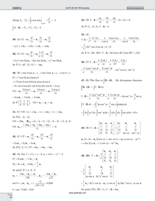

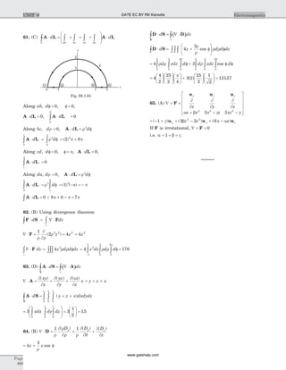
![24. A point charge 20 nC is located at origin. Four
uniform line charge are located as follows 40 nC m at
y = ± 1 and 50 nC m at y = ± 2. The electric flux that
leaves the surface of a sphere, 4 m in radius, centered
at origin is
(A) 1.33 nC (B) 1.89 mC
(C) 1.33 mC (D) 1.89 mC
25. The cylindrical surface r = 8 C contains the surface
charge density, rs
z
e= -
5 20| |
nC m2
. The flux that leaves
the surface r = 8 cm, 1 5cm cm< <z 30 90° < f < ° is
(A) 270.7 nC (B) 9.45 nC
(C) 270.7 pC (D) 9.45 pC
26. Let D u u u= + + +4 2 42 2
xy x z yzx y z( ) C m2
. The
total charge enclosed in the rectangular parallelepiped
0 2 0 3< < < <x y, , 0 5< <z m is
(A) 360 C (B) 180 C
(C) 100 C (D) 560 C
27. Volume charge density is located in free space as
rv
r
e= -
2 1000
nC m3
for 0 1< <r mm and rv = 0
elsewhere. The value of Dr on the surface r = 1 mm is
(A) 1.28 pC m2
(B) 0.28 pC m2
(C) 0.78 pC m2
(D) 0.32 pC m2
28. Spherical surfaces at r = 2 and 4 carry uniform
charge densities of 20 nC m2
and -4 nC m2
. The Dr at
2 4< <r is
(A) -
16
2
r
nC m2
(B)
16
2
r
nC m2
(C)
80
2
r
nC m2
(D) -
80
2
r
nC m2
29. Given the electric flux density, D u u= +2 2
xy xx y
+ 6 3
z zu C m2
. The total charge enclosed in the volume
0 < <x y z a, , is
(A) 6
5
3
5 4
a a+ (B) a a5 4
6+
(C) 6 5 4
a a+ (D)
5
3
65 4
a a+
30. Let D u= 5 4 4 4
x y z y . The flux enclosed by volume
x = 3 and 3.1, y = 1 and 1.1, and z = 2 and 2.1 is
(A) 49.6 (B) 24.8
(C) 35.4 (D) 36.4
31. A spherical surface of radius of 3 mm is centered at
P(4, 1, 5) in free space. If D u= x x C m2
the net electric
flux leaving the spherical surface is
(A) 113.1 mC (B) 339.3 nC
(C) 113.1 nC (D) 452.4 nC
32. The electric flux density is
D u u u= + + -
1
10 5 2 52
2 3 2
z
xyz x z z x yx y z[ ( ) ]
The volume charge density rv at (-2, 3, 5) is
(A) 6.43 (B) 8.96
(C) 10.4 (D) 7.86
33. If D u= 2r r C m2
, the total electric flux leaving the
surface of the cube, 0 0 4< <x y z, , . is
(A) 0.32 (B) 0.34
(C) 0.38 (D) 0.36
34. If E u u u= - +4 3 5x y z in the neighborhood of point
P(6, 2, -3). The incremental work done in moving 5 C
charge a distance of 2 m in the direction u u ux y z+ + is
(A) -60 J (B) 34 64. J
(C) -34 64. J (D) 60 JJ
35. If E u= 100 r V m , the incremental amount of work
done in moving a 60 mC charge a distance of 2 mm from
P(1, 2, 3) toward Q(2, 1, 4) is
(A) -5 4. mJ (B) 3.1 mJ
(C) -31. mJ (D) 0
36. A 10 C charge is moved from the origin to P(3, 1, -1)
in the field E u u u= - +2 3 42
x yx y z V m along the
straight line path x y y x z= - = +3 2, . The amount of
energy required is
(A) -40 J (B) 20 J
(C) -20 J (D) 40 J
37. A uniform surface charge density of 30 nC m2
is
present on the spherical surface r = 6 mm in free space.
The VAB between A ( , , )r = = ° f = °2 35 55cm q and B
( , , )r = = ° f = °3 40 90cm q is
(A) 2.03 V (B) 10.17 V
(C) 4.07 mV (D) -10.17 V
Chap 8.2
Page
471
Electrostatics GATE EC BY RK Kanodia
www.gatehelp.com](https://image.slidesharecdn.com/a-150815031147-lva1-app6892/85/A-gate-by-rk-kanodia-304-320.jpg)
![38. A point charge is located at the origin in free space.
The work done in carrying a charge 10 C from point A
( , , )r = = f =4 6 4q p p to B( , , )r = =4 3 6q p p is
(A) 0.45 mJ (B) 0.32 mJ
(C) -0 45. mJ (D) 0
39. Let a uniform surface charge density of 5 nC m2
be
present at the z = 0 plane, a uniform line charge density
of 8 nC m be located at x z= =0 4, and a point charge
of 2 mC be present at P(2, 0, 0). If V = 0 at A(0, 0, 5),
the V at B(1, 2, 3) is
(A) 10.46 kV (B) 1.98 kV
(C) 0.96 kV (D) 3.78 kV
40. A non uniform linear charge density, rL z= +6 12
( )
nC m lies along the z axis. The potential at P(r = 1, 0, 0)
in free space is ( )V¥ = 0
(A) 0 V (B) 216 V
(C) 144 V (D) 108 V
41. The annular surface, 1 cm < <r 3 cm carries the
nonuniform surface charge density r rs = 5 nC m2
. The V
at P(0, 0, 2 cm) is
(A) 81 mV (B) 90 mV
(C) 63 mV (D) 76 mV
42. If V xy z x y z= + + +2 3 2 32 3 2 2 2
ln( ) in free space the
magnitude of electric field E at P (3, 2, -1) is
(A) 72.6 V/m (B) 79.6 V/m
(C) 75 V/m (D) 70.4 V/m
43. It is known that the potential is given by V r= 70 0 6.
V. The volume charge density at r = 0 6. m is
(A) 1.79 nC m3
(B) -1.79 nC m3
(C) 1.22 nC m3
(D) -1.22 nC m3
44. The potential field V r= 80 2
cos q V. The volume
charge density at point P(2.5, q = °30 , f = °60 ) in free
space is
(A) -2 45. nC m3
(B) 1 42. nC m3
(C) -1 42. nC m3
(D) 2 45. nC m3
45. Within the cylinder r = < <2 0 1, z the potential is
given by V = + + f100 50 150r r sin V. The charge lies
within the cylinder is
(A) -4.94 nC (B) -4.86 nC
(C) -5.56 nC (D) -3.68 nC
46. A dipole having
Qd
4
100 2
peo
= ×V m
is located at the origin in free space and aligned so
that its moment is in the uz direction. The E at point
( , , )r = ° f =1 45 0 is
(A) 158.11 V m (B) 194.21 V m
(C) 146.21 V m (D) 167.37 V m
47. A dipole located at the origin in free space has a
moment p z= ´ -
2 10 9
u C.m. The points at which | |E q
= 1
mV m on line y z x= =, 0 are
(A) y z= = ± 23 35. (B) y z x= = ± =16 5 0. ,
(C) y z= = 16 5. (D) y z x= = =0 23 35 0, . ,
48. A dipole having a moment p u u u= - +3 5 10x y z
nC.m is located at P(1, 2, -4) in free space. The V at Q
(2, 3, 4) is
(A) 1.31 V (B) 1.26 V
(C) 2.62 V (D) 2.52 V
49. A potential field in free space is expressed as
V xyz= 40 . The total energy stored within the cube
1 2< <x y z, , is
(A) 1548 pJ (B) 0
(C) 774 pJ (D) 387 pJ
50. Four 1.2 nC point charge are located in free space at
the corners of a square 4 cm on a side. The total
potential energy stored is
(A) 1.75 mJ (B) 2 mJ
(C) 3.5 mJ (D) 0
51. Given the current density
J u u= +- -
10 2 25 2 2
[sin ( ) cos ( ) ]x e x ey
x
y
y kA m2
The total current crossing the plane y = 1 in the
u y direction in the region 0 1< <x , 0 2< <z is
(A) 0 (B) 12.3 mA
(C) 24.6 mA (D) 6.15 mA
Page
472
ElectromagneticsUNIT 8 GATE EC BY RK Kanodia
www.gatehelp.com](https://image.slidesharecdn.com/a-150815031147-lva1-app6892/85/A-gate-by-rk-kanodia-305-320.jpg)
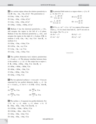
![SOLUTIONS
1. (C) F
R
R
2
1 2 12
12
3
4
=
Q Q
peo | |
=
´ - ´
´
+- -
( )( ) ( )4 10 5 10
4
3 4
5
6 6
3
peo
u ux y
= +( . . )4 32 5 76u ux y mN
2. (D) Arranging the charge in the xy plane at location
(4, 4), (-4, 4), (4, -4), (-4, 4), the fifth charge will be on
the z-axis at location z = 4 2. By symmetry, the force on
the fifth charge will be z directed, and will be four
times the z component
F
q
d
= ´
4
2 4
2
2
peo
= ´
´
´ ´ ´
-
- -
4
2
5 10
4 8 85 10 8 10
9 2
12 3 2
( )
( . )( )p
= -
10 2
N
3. (D) The force will be
F CA
CA
DA
DA
BA
BA
=
´
+ +
é
ë
ê
ù
û
-
( )
| | | | | |
40 10
4
9 2
3 3 3
peo
R
R
R
R
R
R ú
where R u uCA x y= - , R u uDA x y= + , R uBA x= 2
| | | |R RCA DA= = 2, | |RBA = 2
F
u u u u u
=
´
´ ´
-
+
+
+
é
ë
ê
ù-
-
( )
( . )
40 10
4 8 85 10 2 2 2 2
2
8
9 2
9
p
x y x y x
û
ú
= 1376. ux mN
4. (C) E
R
R
R
R
= +
é
ë
ê
ù
û
ú
-
10
4
41 459
13
13
2
23
23
2
peo | | | |
R u u u13 3 4 4= - + -x y z, R u u u23 4 2 5= - +x y z
E
u u u u u u
= ´ ´ ´
- + -
+
+ - +-
9 10 10
41 3 4 4
41
45 4 2 59 9
3 2
(
( )
(
/
x y z x y z
( ) /
45 3 2
é
ë
ê
ù
û
ú
= + +1152 2 93 1089. . .u u ux y z
5. (D) The point is P3(0, y, 0)
R u u u13 4 2 7= - + + -x y zy( ) ,
R u u u12 3 4 2= + - +x y zy( )
E
y y
x =
´ -
+ +
+
´
+ -
é-
10
4
25 4
65 2
60 3
13 4
9
2 3 2 2 3 2
peo
( )
[ ( ) ] [ ( ) ]ë
ê
ù
û
ú
To obtain Ex = 0, 0 48 1392 7312 02
. . .y y+ + =
which yields the two value y = - -6 89 22 11. , .
6. (B) E
R
R
p
AP
AP
=
´ -
2 10
4
6
3
peo | |
=
´ + -é
ë
ê
ù
û
ú
-
2 10
4
4 9 3
106
6
3 2
peo
u u ux y z
( ) /
= + -65 9 148 3 49 4. . .u u ux y z
Then at point P, r = + =8 12 14 42 2
. ,
f = = °-
tan .1 12
8
56 3 , and z = 2
E p p x yr r r= × = × + ×E u u u u u65 9 148 3. ( ) . ( )
= ° + =65 9 56 3 148 3 56 3 159 7. cos . . sin . .
E x yf r f f f= × = × + ×E u u u u u65 9 148 3. ( ) . ( )
= - ° + ° =65 9 56 3 148 3 56 3 27 4. sin . . cos . . ,
Ez = -49 4.
7. (C) E
R
R
R
R
p =
´
- +
é
ë
ê
ù
û
ú
-
2 10
4
28
1
1
3
2
2
3
peo | | | |
R1 = (0, 2, 1) -(0, 0, 0.5) =(0, 2, 0.5)
R2 = (0, 2, 1) - (0, 0, 0) =(0, 2, 1)
E
u u u u
p
y z y z
= ´ ´
- +
+
+é
ë
-
9 10 10
2 0 5
4 25
2 2
5
9 8
3 2 3 2
( . )
( . )
( )
( )
ê
ù
û
ú
E u up y z= +54 9 44 1. .
At P, r = = = °-
5
1
5
63 41
, cos .q and f = °90
So Er p r y r z r= × = × + ×E u u u u u54 9 44 1. [ ] . [ ]
= f + =54 9 44 1 68 83. sin sin . cos .q q
E y zq r q q q= × = × + ×E u u u u u54 9 44 1. [ ] . [ ]
= f + -54 9 44 1. cos sin . ( sin )q q = -14 85.
E y zf f f f= × = × + ×E u u u u ur 54 9 44 1. ( ) . ( ) =54.9 cos f = 0
8. (A) Let a point on y axis be P(0, y, 0)
E
R
R
R
R
p =
´
- -
é
ë
ê
ù
û
ú
-
20 10
4
8
1
1
3
2
2
3
peo | | | |
R1 = (0, y, 0) - (3, 0, 0) =(-3, y, 0)
R2 = (0, y 0) - (-3, 0, 0) = (3, y, 0),
| | | |R R1 2
2
9= = + y
E
u u u u
p
x y x yy
y
y
y
= ´ ´ ´
- +
+
+
+
+
é
ë
ê
ê
-
20 10 9 10
3
9
3
9
9 9
2 3 2 3
( ) ( )
ù
û
ú
ú
=
-
+
1080
9 2 3 2
ux
y( )
, | |E = =
+
1080
9 2 3 2
( )y
9. (B) The field at P will be
E
u u u
p
x y zQ
=
- + -é
ë
ê
ù
û
ú
0
3 2
4
2 2
9peo
, Ez = 1 kV m
Q0
3 2 3
4 9 10 3= - ´ ´ = -pe mo C
10. (C) This will be 8 times the integral of rn over the
first octant
Chap 8.2
Page
475
Electrostatics GATE EC BY RK Kanodia
www.gatehelp.com](https://image.slidesharecdn.com/a-150815031147-lva1-app6892/85/A-gate-by-rk-kanodia-307-320.jpg)
![Q e dxdydzo
x y z
=
¥ ¥ ¥
- - -
ò ò ò8
0 0 0
r = r8 o
11. (C) Q r drd d= fò ò ò0
2
0 0 03
0 05
2
0 2
p p
q q
.
.
. sin
=
é
ë
ê
ù
û
ú4 0 2
3
3
0 03
0 05
p( . )
.
.
r
= 82.1 pC
12. (A) Q
e
z
=
-
+
-
-¥
-¥
òòò
5
10
0 1
2
0
10 .
( | |)r
p
p
p f
=
- -
-
é
ë
ê
ù
û
ú ´
--
5
0 1 1
0 1
0 101 2
0 1
2
0
10
2
e dz
z
.
( . )
( . )
( . )
( )r
p f
+òò-¥
¥
100
2p
Q
dz
z
= ´
+-¥
¥
ò5 26 4
102
.
p2
= ´ ´
é
ëê
ù
ûú =-
-¥
¥
5 26 4
1
10 10
1292 1
. tan .p
z
mC
13. (A)
f = - - ×òòò
°
10 4 5
24
5
0
25
0 9
1 1
2
( )( )sin sin sin
.
.
r r r d dq
f
q r
p
p
q fd
= - +
é
ë
ê
ù
û
ú -
é
ëê
ù
ûú ´ -
°
10
5
9
4
20
3
1
2
1
4
2 2
5 4 3
4
5
0
25
r r r
q qsin cos
.
.
f
p
p
2 0 9
1 1
é
ëê
ù
ûú
= - =10 3 39 0 0266 0 626 0 57[ . ][ . ][ . ] . C
14. (D) E
R
R
p
L p
p
=
r
peo2 2
| |
,
Rp = (1, 2, 3) - (1, -2, 5) = (0, 4, -2)
| |Rp
2
20= ,
E
u u
p
y z
=
´ -é
ë
ê
ù
û
ú
-
5 10
2
4 2
20
9
peo
= -18 9u uy z
15. (C) With z = 0, the general field is
E
u u
z
L y zy
y
= =
+ -
+ +
é
ë
ê
ù
û
ú0 2
2
2 5
2 25
r
peo
( )
( )
we require | | | |E E2 2= y
So 2 2 5( )y + = Þ y =
1
2
E
u u
=
-
+
é
ë
ê
ù
û
ú
6 25
2
2 5 5
6 25 25
. .
.peo
y z
= -9 18u uy z
16. (C) Ep
L Q
Q
Q
Q
= -
é
ë
ê
ù
û
ú
+
+
-
-
r
peo2 2 2
R
R
R
R| | | |
R Q+ = (6, 0, 6) - (0, 3, 6) = (6, -3, 0)
R Q- = (6, 0, 6) - (0, -3, 6) = (6, 3, 0)
E
u u u u
P
x y x y
= ´ ´ ´
-
+
-
+
+
é
ë
ê
ù
û
ú20 2 9 10
6 3
36 9
6 3
36 9
9
nC
= -48u y V m
17. (B) E
R
R
R
R
R
R
P
L xp
xp
yp
yp
zp
zp
= + +
é
ë
ê
ù
û
ú
r
peo2 3 3 3
| | | | | |
Rxp = - - - - =( , , ,) ( , , ,)3 0 1 3 0 0 (0, 2, -1)
Similarly Ryp = (-3, 0, -1), Rzp = (-3, 2, 0)
Ep = ´ ´ ´ ´- -
100 10 2 9 109 9
E
u u u u u
p
y z x z x yu
= ´ ´ ´ ´ ´
-
+
- -
+
- +é- -
100 10 2 9 10
2
5
3
10
3 2
13
9 9
ë
ê
ù
û
ú
= - + -0 96 0 54. .u u ux y z kV m
18. (C) At y L
y= =4
2
, E u
r
peo
,
d dq dzLF E E= = r
F
u
= ò0
1 2
2
6
r
peo
L ydz
( ) = 18 75. u y mN
19. (A) E
dSs
=
- ¢
- ¢ò ò
r
peo4 3
R R
R R| |
where R u= 3 x and R u u¢ = +y zy z ,
E
u u
PA
L x y zy zu
y z
dydz=
- -
+ +--¥
¥
òò
r
peo4
3
9 2 2 3 2
2
2
( )
Due to odd function
E
u
PA
L x dydz
y z
=
+ +--¥
¥
òò
r
peo4
3
9 2 2 3 2
2
2
( )
So there is only x component.
20. (D) There will be z component of E only
R u R u= ¢ =z z , r r , R R u u- ¢ = -z z zr
E
z d d
z
z P
s
a,
.
( )
=
+òò
r
pe
r r f
ro
p
4 2 2 3 2
0
0 2
0
2
=
+
é
ë
ê
ê
ù
û
ú
ú
= -
+
é
ë
ê
ê
2pr
pe r
r
eo o
s sz
z
z
z z4
1 1 1
0 042 2
0
0 2
2 2
.
.
ù
û
ú
ú
E
z
z
z
s
= -
+
é
ë
ê
ê
ù
û
ú
ú
r
eo
1
0 042
.
, at z = 0 5. , Ez = 20 2. V m
21. (A) Since charge sheet are infinite, the field
magnitude associated with each one will be r eos 2 ,
which is position independent. The field direction will
depend on which side of a given sheet one is positioned.
EA x y z=
´
-
´
-
´é
ë
ê
ù
û
ú
- - -
10 10
2
40 10
2
50 10
2
9 9 9
e e eo o o
u u u
= + -0 56 2 23 2 8. . .u u ux y z
Page
476
ElectromagneticsUNIT 8 GATE EC BY RK Kanodia
www.gatehelp.com](https://image.slidesharecdn.com/a-150815031147-lva1-app6892/85/A-gate-by-rk-kanodia-308-320.jpg)
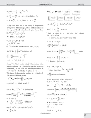
![= - - +ò10 2 3 42
( )x yx y zu u u ( )dx dy dzx y zu u u+ +
= - + -ò ò ò
-
10 2 10 3 10 4
0
3
2
0
1
0
1
xdx y dy dz = -40 J
37. (D) rA = 2 cm, rB = 3 cm
V r
Q
r
a
r
s
( ) = =
4
4
4
2
pe
p r
peo o
=
´ ´ ´
´ ´
- -
-
( )
.
6 10 30 10
8 85 10
3 2 9
12
r
V r
r
( )
.
=
0 122
, V V VAB A B= - = =
0 122
0 02
0 122
0 03
.
.
.
.
= 2 03.
38. (D) W
Q Q dr
r
Q Q
r rr
r
B AA
B
= - = -
é
ë
ê
ù
û
úò1 2
2
1 2
4 4
1 1
pe peo o
r rA B= , W = 0
39. (B) V s
Q
r
P ( ) =
4peo
,
V
d
C Cl
L L
( ) lnr
r r
pe r
r
pe
r
o o
= - + = - +ò 2 2
1 1
V z dz C
z
Cs
s s
( ) = - + = +ò
r
e
r
eo o2 2
2 2
V
Q
r
z CL s
= - - +
4 2 2pe
r
pe
r
r
peo o o
ln
Here r z, ,r are the scalar distance from the charge.
r = + =2 5 292 2
, r = - =( )5 4 12
, z = 5
By putting these value. C = - ´193 103
.
At point N, r z= - + + =( )2 1 2 142 2 2
r = + =1 1 22 2`
, z = 3, VB = 198. kV
40. (D) V
dz
R
dz
z
L
r
o o
r
pe pe
= =
´
+
=
-¥
¥ -
-¥
¥
ò ò4
6 10
4 1
108
9
2 3 2
( )
V
41. (A) V
dS
| |
s
r
o
r
pe
=
- ¢òò 4 R R
,
R u R u= ¢ =z z, r r, dS d d= fr r ,
V
d d
z
r
p
o
r r
pe r
=
´ f
+
ò ò
-
0
2 9 2
2 2
0 01
0 03
5 10
4
( )
.
.
,
V z
z
zp =
´
+ - + +
é
ë
ê
ù
û
ú
-
5 10
2 2 2
9
2 2
2
2 2
0 01
0 03
e
r
r r r
o
ln ( )
.
.
At z = 0 02. , Vp = 0 081. V
42. (C) E = -ÑV
= - +
+ +
é
ë
ê
ù
û
ú2
6
2 3
2 2
2 2 2
y z
x
x y z
xu
- +
+ +
é
ë
ê
ù
û
ú4
12
2 3
3
2 2 2
xyz
y
x y z
yu
- +
+ +
é
ë
ê
ù
û
ú6
18
2 3
2 2
2 2 2
xy z
z
x y z
zu
E u u up x y z= + -7 1 22 8 711. . . V m,
| |E = 75 V m
43. (D) E u u= -Ñ = - = - -
V
dV
dr
rr r( . )( ) .
0 6 70 0 4
= - -
42 0 4
r r
.
u V m,
D E u= = - -
e eo o42 0 4
r r
.
C m2
r eov r
r
d
dr
r D
r
d
dr
r= Ñ × = = -D
1 1
422
2
2
1 6
( ) ( ).
= - 67 2 1 4
. .
eo
r
At r = 0 6. m,
rv = -
´ ´
= -
-
67 2 8 85 10
0 6
1 22
12
1 4
. .
( . )
..
nC m3
44. (A) E u u= -Ñ = - -V
V
r r
V
r
¶q
q
1
= - +160 80r rrcos sinq q qu u V m
D E u u= = - -e e q qo o q80 2( cos sin )r rr
r
¶ q ¶q
qv r r
r r
r D
r
D= Ñ × = +
¶é
ë
ê
ù
û
úD
1 2 1
2
2
( )
sin
( sin )
r e q
q q
q
ov
r
r
r
= - ´ -
é
ë
ê
ù
û
ú80
1
2 3
122
cos
sin cos
sin
r e qoV = - = -320 2 45cos . nC m3
45. (C) E u u= -Ñ = - - fV
V V
¶r r
¶f
r
1
= - + f - f f( sin ) ( cos )50 150 150u ur ,
D = eo E, r eov = Ñ × = Ñ ×D E
r e
r
¶r
(r
r
¶f
o rv E E= +
é
ë
ê
ù
û
úf
1 1
)
= -
+ f
+
fé
ë
ê
ù
û
úe
r r
o
( sin ) sin50 150 150
= -
50e
r
o
C m2
Q d d dz= fòòò
50
0
2
0
2
0
1
e
r
r ro
p
= - = -2 50 2 5 56p eo( ) . nC
46. (A) V
Qd
r r
= =
cos cosq
pe
q
o4
100
2 2
,
E u u= -Ñ = - +
æ
è
ç
ö
ø
÷V
V
r r
V
r
¶q
q
1
= +
100
23
r
r( cos sin )q q qu u ,
| |E = +100 4 2 2 1 2
( cos sin )q q = ´ =100
5
2
158 11. V m
47. (A) E u u=
´
+
-
2 10
4
2
9
3
pe
q q
o
q
r
r[ cos sin ],
Page
478
ElectromagneticsUNIT 8 GATE EC BY RK Kanodia
www.gatehelp.com](https://image.slidesharecdn.com/a-150815031147-lva1-app6892/85/A-gate-by-rk-kanodia-310-320.jpg)
![y z= lies at q = 45°
E
r
q
ope
=
´
=
-
-2 10
4
1
2
10
9
3
3
(required)
r3 3
12 73 10= ´. , r = 23 35.
48. (A) V
| |
=
× - ¢
- ¢
P R R
R R
( )
4 3
peo
where R R Q P- ¢ = - = (1, 1, 8)
So VP
x y z x y z
=
- + × + + ´
+ +
-
( ) ( )
( ) .
3 5 10 8 10
4 1 1 8
9
2 1 5
u u u u u u
peo
=1.31 V
49. (A) E = -ÑV = + +
é
ë
ê
ù
û
ú40
1 1 1
2 2 2
x yz xy z xyz
x y zu u u
W dve = ×òòò
eo
2
E E
W
x y z x y z x y z
dxdye = + +
é
ë
ê
ù
û
úò ò ò800
1 1 1
1
2
1
2
1
2
4 2 2 2 4 2 2 2 4
eo dz
= 1548 pJ
50. (A) W q Vn n
n
=
=
å
1
2 1
4
V V V V1 21 31 41= + + = + +
é
ëê
ù
ûú
q
4
1
0 04
1
0 04
1
0 04 2peo . . .
V V V V1 2 3 4= = =
W q V=
1
2
4 1 1( ) =
´ ´
+
é
ëê
ù
ûú
-
2 1 2 10
4 0 04
2
1
2
9 2
( . )
( . )peo
= 175. mJ
51. (B) I dS dxdzy
S
y y
= × = ×= =òò òòJ n J u1 1
0
1
0
2
= -
òò 10 2 25 2
0
1
0
2
cos ( )x dxdzy
= 12307 kA = 12 3. MA
52. (C) I dS
S
= ×òòJ n
=
+òò
800
0 80 4
0 802
2
0 1
0 3
0
2
sin
( . )
( . ) sin
.
.
q
q q f
p
pp
d d =154.8 A
53. (D) F ma qE= = ,
a
qE
m
z= =
- ´ - ´
´
-
-
( . )( )
.
1 602 10 4 10
9 11 10
19 6
3
u = ´7 0 1017
. uz m s2
,
v at t z= = ´7 0 1017
. u m s
54. (D)
¶r
V
t
= - Ñ × J =
+
¶1
r ¶r
r
r( )J
J
z
z
=
+
¶ -
+
æ
è
çç
ö
ø
÷÷ =
1
25
20
0 01
02
r ¶r ¶ r
( )
.z
55. (A) I dSz
S
= × =òòJ n 0 2.
=
+
f = +òò
40
0 1
40
2
0 1 22 2
0
0 4
0
2
2 2
0
0 4
r
r r r
p
( . )
log[ ( . ) ] (
. .
d d p)
= 40 17p log = 356 A
56. (B) So E E
J J
al st
al
al
st
st
= = =
s s
Þ J Jal
ac
st
st=
s
s
I J Jst al= ´ + ´ - ´- - -
p p( ) [( ) ( ) ]2 10 4 10 2 103 3 2 3 2
= 80
Solving Jst = ´3 2 105
. A m2
57. (B) J
l
=
4
2pr
ru A m2
,
E
J
l l
= = =
s pr s r
r
4
2
12 73.
u V m
V d
l
d= - × = ×ò òE L u u
5
3
3
5
12 73.
r
rr r = =
12 73 5
3
6 51.
ln
.
l l
V
R
V
I l
= = =
6 51
4
1 63. .
r
W
58. (D) E u u u= -Ñ = - + +
æ
è
çç
ö
ø
÷÷fV
V V V
z
z
¶r r
¶f
r
1
= - f +
+
f - + ffz z z z
2 21
2 1cos
( )
sin ( ) cosu u ur
r
r
r
E u u u= - + -f f1 82 14 5 2 67. . . z V m
r e eo os s
| |
= × =
×
E n
E E
E
r eos = + + =1 82 14 5 2 67 13152 2 2
. . . . pC m2
59. (C) V = =
40
3 2
2
2 53
cos sin
.
p p
V
So the equation of the surface is
40
2 52
cos sin
.
q f
=
r
, 16 3
cos sinq f = r
60. (A) E = -ÑV, D E= = - Ñe eo V
= -
+
+
+
é
ë
ê
ù
û
úe
o 200
4
200
42 2
z
x
x
x
x
x
x z
( )
u u C m2
D u( )z z
x
x
= = -
+
0 2
200
4
eo
C m2
,
r
eo
s z z
x
x
= × =
-
+=
D u 0 2
200
4
C m2
,
Q
x
x
dxdy x=
-
+
= - +òò-
200
4
3 200
1
2
42
0
2
3
0
2
0
2
e
eo
o( )( ) ln[ ]
= - = -300 2 1 84ln . nC
Chap 8.2
Page
479
Electrostatics GATE EC BY RK Kanodia
www.gatehelp.com](https://image.slidesharecdn.com/a-150815031147-lva1-app6892/85/A-gate-by-rk-kanodia-311-320.jpg)
![61. (B) E = -ÑV , -3 2 3
xy z satisfy this equation.
62. (D) The plane can be replaced by -60 nC at Q (2, 5,
-6).
R = (5, 3, 1) - (2, 4, 6) = (3, -1, -5)
¢ =R (5, 3, 1)-(2, 4, -6) = (3, -1, 7),
| | , | |R R= ¢ =35 59
V
q
R
q
R
q
P = -
¢
= -
é
ëê
ù
ûú4 4 4
1
35
1
59pe pe peo o o
Vp = ´ ´ ´ -
é
ëê
ù
ûú =- -
60 10 9 10
1
35
1
59
219 9
V
63. (A) Using method of images
V Vp
L
- = -0
2
r
peo
ln
Final Distance from the charge
Initial Distance from the charge
é
ë
ê
ù
û
ú
V0 0= ,
Vp
L
= - +
+ -
-
+ - -
-
+r
peo2
1
2
1 2 1
1
1 2 2
1
1 32 2 2 2 2
ln ln
( )
ln
( ( ))
ln
2
1
é
ë
ê
ê
ù
û
ú
ú
= 2.40 kV
64. (C) P D E D
D D
= - = - = -e
e e
eo
r r
r( )1
P u u u= - +
- ´ -
( )
( . )
.
2 4 5
2 4 1 10
2 4
9
x y z
P u u u= - +12 2 3 2 9. . .x y z nC m2
65. (C) D Dn n1 2= Þ e e1 1 2 2E EN N=
= ´ =2 15 2 5 2. .e eo o En Þ En 2 12= .
E Et t1 2= , E u u u2 1 2 3 1= - +. x y z
66. (D) The unit vector that is normal to the surface is
u
u u u
N
x y zF
F
=
Ñ
Ñ
=
- +
| |
2
6
,
En N1 1
1
6
100 200 100 817= × = - - = -E u [ ] . V m
E u u un x y z1 817
1
6
2= - - +. [ ]
= - + -33 33 33 33 66 67. . .u u ux y z V m
E E E u u ut n x z z1 1 1 133 3 166 7 16 67= - = + +. . .
E Et t1 2= and D Dn n1 2=
Þ =e e e eo or n r n1 1 2 2E E
E E En
r
r
n n2
1
2
1 1
1
4
= =
e
e
, E E E2 2 1
1
4
= +t n
= + + - + -1333 1667 1667 833 833 1667. . . . . .u u u u u ux y z x y z
= +125 175u ux y V m
67. (B) D Dn n1 2= , e e e eo or n r n1 1 2 2E E=
Since E is normal to the surface
E E u un
r
r
n r r
r r
2
1
2
1 2 2
2
5
1000 400
= = ´ =
e
e
V m
68. (D) D Dn n1 2= and E Et t1 2= , D E= e
D D En n n1 2 180 3 5= ´ = =e eo o , En1 48=
E u u u2 48 60 40= - -x y z
69. (A) D E= = - Ñe f x V( ) ,
Ñ × = = = Ñ × - ÑD f x Vvr 0 ( ( ) )
0 = Ñ × - Ñ( ( ) )f x V
= - + + +
é
ë
ê
ù
û
ú
dF
dx
V
x
f x
V
x
f x
V
y
f x
V
z
( ) ( ) ( )
2
2
2
2
2
2
= - + Ñ
é
ëê
ù
ûú
dF
dx
V
x
f x V
( ) 2
Þ Ñ = -2 1
V
f x
dF
dx
V
x( )
70. (A) rv = 0 Þ Ñ =2
0V ,
Ñ = + - =2 2
2
2
16 6 0V e
f
x
x 
f
x
e x
= - +16 62
Þ
f
x
e x Cx
= - + +8 62
1
E
V
x
e
f
x
x
x
= = +
8 2
E
f
x
f
x
x
x x
( )0 8 0 8
0 0
= + = Þ = -
= =
It follow that C1 0=
Integrating again
f x e x Cx
( )1
2 2
4 3= - + + , f C( , )0 1 4 2= - +
V f( , ) ( )0 0 0 4 0= = + Þ C2 0= . f ( )0 4= -
f x e xx
( ) = - +4 32 2
,
V x y e e x yx x
( , ) = - + -4 4 3 32 2 2 2
= -3 2 2
( )x y
*********
Page
480
ElectromagneticsUNIT 8 GATE EC BY RK Kanodia
www.gatehelp.com](https://image.slidesharecdn.com/a-150815031147-lva1-app6892/85/A-gate-by-rk-kanodia-312-320.jpg)
![Statement for Q.9–11:
An infinite filament on the z-axis carries 10 mA in
the uz direction. Three uniform cylindrical current
sheets are also present at 400 mA m at r = 1 cm, -250
mA m at r = 2 cm and 300 mA m at r = 3 cm.
9. The magnetic field Hf at r = 0.5 cm is
(A) 0.32 A m (B) 0.64 A m
(C) 1.36 mA m (D) 0
10. The magnetic field Hf at r = 15. cm is
(A) 1.63 A m (B) 0.37 A m
(C) 2.64 A m (D) 0
11. The magnetic field Hf at r = 3.5 cm is
(A) 0.14 A m (B) 0.56 A m
(C) 0.27 A m (D) 0.96 A m
Statement for Q.12–14:
In the fig. P8.3.12–14 The region 0 2£ £z is filled
with an infinite slab of magnetic material (mr = 2 5. ). The
surface of the slab at z = 0 and z = 2, respectively, carry
surface current 30ux A m and -40ux as shown in fig.
12. In the region 0 2< <z the H is
(A) -35u y A m (B) 35u y A m
(C) -5u y A m (D) 5u y A m
13. In the region z < 0 the H is
(A) 5u y A m (B) -5u y A m
(C) 10u y A m (D) -10u y A m
14. In the region z > 2 the H is
(A) 5u y A m (B) -5u y A m
(C) 35u y A m (D) -35u y A m
Statement for Q.15–16:
In the cylindrical region
H
H
f
f
r
r
r .
r
r .
= + £
= >
2
2
0 6
3
0 6
for
for
15. The current density J for r < 0 6. mm is
(A) 2uz A m (B) -2uz A m
(C) uz A m (D) 0
16. The current density J for r > 0 6. mm is
(A) 2uz A m (B) -3uz A m
(C) 3uz A m (D) 0
17. An electron with velocity
v u u u= + - ´( )3 12 4 105
x y z m s experiences no net
forces at a point in a magnetic field B u u u= + +x y z2 3
mWb m2
. The electric field E at that point is
(A) - + +4 4 1 3 0 6. . .u u ux y z kV m
(B) 4 4 1 3 0 6. . .u u ux y z- - kV m
(C) - + +4 4 1 3 0 6. . .u u ux y z kV m
(D) 4 4 1 3 0 6. . .u u ux y z- - kV m
18. A point charge of 2 10 16
´ -
C and 5 10 26
´ -
kg is
moving in the combined fields B u u u= - + -3 2x y z mT
and E u u u= - +100 200 300x y z V m. If the charge
velocity at t = 0 is v u u u( ) ( )0 2 3 4 105
= - -x y z m s, the
acceleration of charge at t = 0 is
(A) 600 3 2 3 109
[ ]u u ux y z+ - m s2
(B) 400 6 6 3 109
[ ]u u ux y z+ - m s2
(C) 400 6 6 3 109
[ ]u u ux y z- + m s2
(D) 800 6 6 109
[ ]u u ux y z+ - m s2
19. An electron is moving at velocity v u= ´4 5 107
. y
m s along the negative y-axis. At the origin, it
encounters the uniform magnetic field B u= 2 5. z mT,
and remains in it up to y = 2 5. cm. If we assume that the
electron remains on the y –axis while it is in the
magnetic field, at y = 50 cm the x and z coordinate are
respectively
(A) 1.23 m, 0.23 m (B) -1.23 m, -0.23 m
(C) -11.7 cm, 0 (D) 11.7 cm, 0
Page
482
ElectromagneticsUNIT 8
z
x
z=2
mo
z=0
-40 A/mux
30 A/mux
mr = 2.5
mo
Fig. P8.3.12–14
GATE EC BY RK Kanodia
www.gatehelp.com](https://image.slidesharecdn.com/a-150815031147-lva1-app6892/85/A-gate-by-rk-kanodia-313-320.jpg)
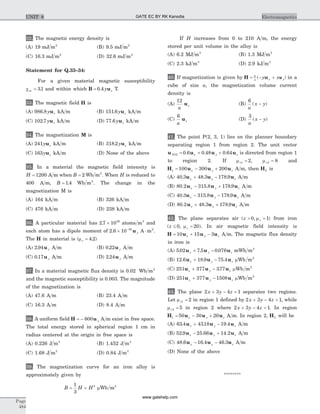
![SOLUTIONS
1. (C) H
L u
=
´
-¥
¥
ò
Id
R
R
4 2
p
=
- + -
+ -
=
¥
ò
I dy y
y
y x y
4
2 3
2 32 2 3 2
0
p
u u u[ ( ) ]
[ ( ) ]
=
+ -
¥
ò
I dy
y
z
4
2
2 32 2 3 2
0
p
u
[ ( ) ]
3 2- =y tan q, - =dy 2 2
sec q,
q1 = 56.31°, q2 90= - °
H
u
=
- °
°
ò
I dz
4
2
290
56 31
p
q
q
.
sec
= =- °
°I
z z
4
145 890
56 31
p
qu u[sin ] ..
mA m
2. (A) H H H= +y z , H uz
zI
= f
2pr
r = - + =( ) ( )3 4 52 2
u
u u u u u
f =
- ´ - +
=
+z x y y x( )3 4
5
3 4
5
H
u u
u uz
x y
x y=
+
= +
24
2 5
4 3
5
0 611 0 458
p( )
( )
. . mA m
H uy
yI
= f
2pr
, r = - + =( ) ( )3 5 342 2
u u
u u u u
f = ´
- +
=
-
y
x z z x( )3 5
34
3 5
34
H
u u
y
x z
=
- +12
2 34
5 3
34p
( )
= - +0 281 0 168. .u ux z mA m
H H H u u u= + = + +y z x y z0 331 0 458 0 168. . . mA m
3. (A) H = -
´ -
+
f
-
ò
I Idz z
z
z z
2 4 2 2 3 2
4
4
pr
r
p r
r
u
u u u( )
( )
I I dz
z2 4 4 2 2 3 2
4
4
pr p
r
p r
u uf
-
f-
+ò ( )
= -
+
f f
I I
2 4
8
162pr p r r
u u
( )
= -
+
æ
è
ç
ç
ö
ø
÷
÷ f
I
2
1
4
162pr r( )
u
At r = - f = °3 60, , I = 3p,
H u= f0 1. A m
4. (B) H
u
=
´
ò
Id
R
RL
4 2
p
, Id dx xL u= 4
uR
x y zx
R
=
- + + +( )1 3 2u u u
R x= + + +( )1 3 22 2 2
= + +x x2
2 14
H
u u u u
=
´ - + + +
+ +-¥
¥
ò
4 1 3 2
4 2 142 3 2
dx x
x x
x x y z[ ( ) ]
( )p
=
-
+ +
=
-
-¥
¥
ò
( )
( )
( )
/
12 8
4 2 14
2 12 8
4 132 3 2
u u u uz y z ydx
x xp p
= -0 147 0 098. .u uz y A m
5. (B) H = -
´ -
+
f
-
ò
I Idz z
z
z z
a
a
2 4 2 2 3 2
pr
r
p r
r
u
u u u( )
( )
= -
+
f
-
ò
I Idz
za
a
2 4 2 2 3 2
pr
r
p r
f
u
u
( )
r
p r
r
p r r p
f f fIdz
z
I z
z
Ia
a
a
a
a
u u u
4 4 22 2 3 2 2 2 2 3 2
( ) ( )+
=
+
=
- -
ò r r( )2 2 3 2
+ z
= -
+
æ
è
ç
ç
ö
ø
÷
÷ f
I a
a2
1
2 2pr r( )
u A m
At r = 1, H
I
=
2pr
Þ -
+
=1
1
1
22
a
a
Þ a =
1
3
= 0.577 m
6. (A) H
u
=
´
ò
Id
R
RL
4 2
p
=
f ´ -f
ò
Id
a
u u( )r
p
p40
2
=
I
a
z
2
u A m
I = 3 A, a = 0 5. m, H u= 3 z A m
7. (D) H
u
=
´
òò
K Rdxdy
R4 2
p
=
´ - - -
+ +-¥
¥
-
òò
4 3
4 92 2 3 2
2
2
u u u ux x y zx y dx dy
x y
( )
( )p
=
- -
+ +-¥
¥
-
òò
4 3
4 92 2 3 2
2
2
( )
( )
y dx dy
x y
z yu u
p
=
+ +-¥
¥
-
òò
12
4 92 2 3 2
2
2
u ydx dy
x yp( )
= -
+-
ò
3 2
92
2
2
p
u y
y
dy
-
æ
è
ç
ö
ø
÷
-
-
6 1
3 3
1
2
2
p
u y
y
tan = -0 75. u y A/m
Chap 8.3
Page
485
Magnetostatics GATE EC BY RK Kanodia
www.gatehelp.com](https://image.slidesharecdn.com/a-150815031147-lva1-app6892/85/A-gate-by-rk-kanodia-316-320.jpg)
![8. (D) H
u
=
´
ò
Id
R
RL
4 2
p
=
- ´ - +
+
+
´ - +
+
Idz z
z
Idx x
x
z z y x x yu u u u u u( )
( )
( )
(4 1 4 12 3 2 2
p p )3 2
00
¥¥
òò
=
+
+
+
¥¥
òò
Idz
z
Idx
x
x zu u
4 1 4 12 3 2 2 3 2
00
p p( ) ( )
=
+
+
+
æ
è
ç
çç
ö
ø
÷
÷÷¥ ¥
I z
z
x
x
x z
4 1 12
0
2
0
p
u u
( ) ( )
= + = +
I
x z x z
4
0 8
p
( (u u u u) . ) mA m
9. (A) Using Ampere’s circuital law
H L× = =ò fd H Iencl2pr
At r = 0 5. cm, Iencl = 10 mA
2 5 10 103
p( )´ =-
fH , Hf = 0 32. A m
10. (B) At r = 15. cm enclosed current
Iencl = + =10 2 0 01 400 35 13p( . )( ) . mA
2 0 015 35 13 10 3
p( . ) .Hf
-
= ´ Þ Hf = 0 37. A m
11. (C) The enclosed current is
Iencl = + - +10 2 0 01 400 2 0 02 250 2 0 03 300p p p( . ) ( . ) ( . )
= 60 3. mA m
2 0 035 60 3p( . ) .Hf = M Þ Hf = 0 27. A m
12. (A) H u u u= - - ´ - = -
1
2
30 40 35( ) ( )x z y A m
13. (B) H K u= ´
1
2
n
= - ´ - = -
1
2
30 40 5( ) ( )u u ux z y A m
14. (A) H u u u= - + + - =
1
2
30 40 5( ) ( )x z y A m
15. (C) J H u= Ñ ´ = f1
r
¶ r
¶r
( )H
z
= +
æ
è
çç
ö
ø
÷÷
1
2
2
2
r
¶r
r
uz = uz A m
16. (D) J =
æ
è
çç
ö
ø
÷÷ =
1 3
0
r
¶r
r
r
17. (A) F E v B= + ´e( )
If F = 0, E v B B v= - ´ = ´
u u ux y z
1 2 3
3 12 4
10 105 3
-
é
ë
ê
ê
ê
ù
û
ú
ú
ú
´ ´ -
= - - - - - + - ´[ ( ) ( ) ( )]u u ux y z8 36 4 9 12 6 102
V m
= - + +4 4 1 3 0 6. . .u u ux y z kV m
18. (D) v B u u u( ) ( )0 2 3 4 105
´ = - -x y z
´ - + - -
( )3 2 10 3
u u ux y z
= + -1100 1400 500u u ux y z
F E v B( ) [ ]0 = + ´Q
= ´ + --
2 10 1200 1200 20016
[ ]u u ux y z
= ´ + --
4 10 6 614
[ ]u u ux y z
F a= m Þ a
F
=
m
=
´
´
+ -
-
-
4 10
5 10
6 6
14
26
[ ]u u ux y z
= + -800 6 6 109
[ ]u u ux y z m s2
19. (C) F v B= ´e
= - ´ ´ ´- -
( . )( . )( . )1 6 10 4 5 10 2 5 1019 7 3
u uy z
= - ´ -
1 8 10 14
. ux N
This force will be constant during the time the electron
travels the field. It establishes a negative x –directed
velocity as it leaves the field, given by the acceleration
times the transit time tt ,
v
Ft
m
x
t
= =
- ´
´
æ
è
çç
ö
ø
÷÷
´
´
-
-
-
1 8 10
9 1 10
2 5 10
4 5 10
14
31
2
7
.
.
.
.
æ
è
çç
ö
ø
÷÷ = - ´11 107
. m s
t50 7
80 5 0 025
4 5 10
106 10=
-
´
= ´ -. .
.
. s
In that time, the electron moves to an x coordinate
given by
x v tx= = - ´ ´ = --
50
7 8
11 10 106 10 0 117( . )( . ) . m
x = -117. cm, z = 0
20. (A) FBC
B
C
I d= ´ò loop from wire at BCL B
= ´ ´ = - ´ = -- -
ò( )
( )
.6 10
2 3
1 8 10 183
1
4
8
dz z y x xu u u u
15m
p
o
nN
21. (C) The field from the long wire now varies with
position along the loop segment.
F u uAB x ydx
x
= ´ ´-
ò( )6 10
15
2
3
1
3
m
p
o
=
´ -
45 10
3
3
p
mo ln uz = 19 8. uz nN
Page
486
ElectromagneticsUNIT 8 GATE EC BY RK Kanodia
www.gatehelp.com](https://image.slidesharecdn.com/a-150815031147-lva1-app6892/85/A-gate-by-rk-kanodia-317-320.jpg)
![22. (A) This will be the vector sum of the forces on the
four sides. By symmetry, the forces on sides AB and CD
will be equal and opposite, and so will cancel. This
leaves the sum of forces on side BC and DA
F u u uDA z y xdx= - ´ ´ =-
ò ( )
(
6 10
15
2 1
543
1
4
m
p )
o
nN
F F Ftotal DA BC= + = - =( )54 18 36u ux x nN
23. (A) F L R= ´òId
= ´ + ´ + ´ + ´ò ò ò òI dx I dy I dx I dyx y x yu B u B u B u B
1
2
1
2
1
3
2
1
u B u u u ux x x y zx y z´ = - +[ ]6 9 3 = -3 9z yy zu u
u B u u u uy y x y zx y z´ = - +[ ]6 9 3 = -3 6z xx zu u
z = 0 for all element
F = - + - + -= = =ò òI dx y I dy x I dx yz y z x z y( ) ( ) ( )9 6 91
1
3
3
1
2
2
3
u u u
1
1
2
1
6ò ò+ - =I dy x z x( )u
= - - + + = ´ =I z z z( )18 18 36 6 5 6 30u u u N
24. (B) Within the region - < <1 1y , the magnetic fields
from the two outer sheets (carrying -4uz A m) cancel,
leaving only the field from the center sheet. Therefore
H u= -4 x A m ( )0 1< <y and H u= 4 x A m ( )- < <1 0y .
Outside (y > 1 and y < - 1) the fields from all three sheet
cancel, leaving H y y= > < -0 1 1( , ). So at x = 0, y = 0 5.
F
u B
m
I z= ´ = ´ ´ - = --
( ) .7 10 4 35 23
u u uz x ymo nN m
25. (D)
F
u u
m
I x x= ´ - =( )4 0mo
26. (A) F L B= ´òId
0
1
= ´
-
´
=ò -
100
100
2 5 10
0 4
0
1
3
dz z
y
xu
u
u
m
p
o
( )
. N m
27. (B) The field from the current strip at the filament
location
B
u
= ò
6
20 5
1 5
m
p
o x
y
dy
.
.
=
æ
è
ç
ö
ø
÷
3 15
0 5
m
p
o
ln
.
.
ux
= ´ -
1 32 10 6
. ux Wb m2
F L B= ´òId
0
1
= ´ ´ =-
ò5 1 32 10 6 66
0
1
dz dzz x yu u u. . mN m
28. (A) F = ´òK BdS
area
= ´
-
òò 6
5
20 5
1 5
0
1
u
u
z
x
y
dy
m
p
o
.
.
= -
æ
è
ç
ö
ø
÷ = -
15 15
0 5
6 6
m
p
o
ln
.
.
.u uy y mN m
29. (A) c mm r+ =1 , cm + =1 6 5. , cm = 5 5.
30. (A) B H H= =m m mo r
= ´ ´ + --
4 10 6 5 10 25 407
p . ( )u u ux y z
= + -82 204 327u u ux y z mWb m2
31. (C) M H u u u= = + -cm x y z55 137 5 220. A m
32. (B) W = ×
1
2
H B =
1
2
2
mH
= ´ ´ ´ + + =-1
2
6 5 4 10 100 625 1600 9 57
. ( ) .p mJ m2
33. (D) m cr m= + = + =1 31 1 4 1. . , m m m mo o= =r 4 1.
H
B u
u= =
´ ´
=-
m p
0 4
4 1 4 10
77 67
.
.
.
y
yz
z kA m
34. (A) M H u u= = =cm z zy y( . )( . )31 77 6 241 kA m
35. (C) For case 1, m = =
B
H
1 2
1200
m
m
m po
r1 7
1
600
1
4 10
1326 3= = ´
´
=-
.
c mm r= - =1 1325 3.
M Hm1 1
6
1590 10= = ´c . A m
For case 2, m = =
B
H
2
2
1 4
400
.
m
p
r1 7
1 4
400 4 10
2785 2=
´ ´
=-
.
.
cm = 2784 2. 2784.2
M Hm2 2
6
1114 10= = ´c . A m
DM = - ´ =( . . )1590 1114 10 4766
kA m
36. (B) M m u= = ´ ´ -
N y( . )( . )2 7 10 2 6 1029 30
= 0 7. u y A m
H
M u
u=
-
=
-
=
mr
y
y
1
0 7
4 2 1
0 22
.
.
. A m
37. (A) M
B
= +
æ
è
çç
ö
ø
÷÷
-
m co
1
1
1
m
Chap 8.3
Page
487
Magnetostatics GATE EC BY RK Kanodia
www.gatehelp.com](https://image.slidesharecdn.com/a-150815031147-lva1-app6892/85/A-gate-by-rk-kanodia-318-320.jpg)
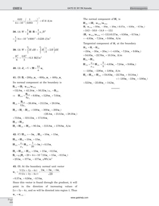
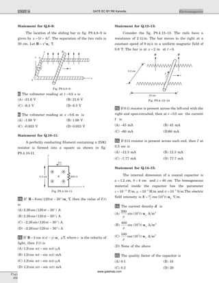
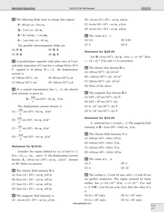
![27. For distilled water m mo= , e eo= 81 , and s = ´ -
2 10 3
S m, the ratio of conduction current density to
displacement current density at 1 GHz is
(A) 111 10 5
. ´ -
(B) 4 44 10 4
. ´ -
(C) 2 68 10 6
. ´ -
(D) 1 68 10 7
. ´ -
28. A conductor with cross-sectional area of 10 cm2
carrier a conductor current 2 109
sin ( )t mA. If
s = ´2 5 106
. S m and er = 4 6. , the magnitude of the
displacement current density is
(A) 48.4 m A m2
(B) 8.11 nA m2
(C) 32.6 nA m2
(D) 16.4 m A m2
29. In a certain region
J u u u= + +( ) sin ( )4 2 103 4
y xz z tx y z A m
If volume charge density rv in z = 0 plane is zero,
then rv is
(A) 3 102 4
z tcos ( ) mC m3
(B) 0 3 102 4
. cos ( )z t mC m3
(C) -3 102 4
z tcos ( ) mC m3
(D) -0 3 102 4
. cos ( )z t mC m3
30. In a charge-free region (s = 0, e e eo= r, m mo= )
magnetic field intensity is H u= -10 10 411
cos ( )t y z
A m. The displacement current density is
(A) - -40 10 49
sin ( )t y yu A m
(B) 40 10 49
sin ( )t y y- u A m
(C) - -40 10 43
sin( )t y xu A m
(D) 40 10 49
sin ( )t y x- u A m
31. In a nonmagnetic medium ( . )er = 6 25 the magnetic
field of an EM wave is H u= 6 108
cos cos ( )bx t z A m.
The corresponding electric field is
(A) 903 0 83 108
sin ( . ) sin ( )x t V m
(B) 903 12 108
sin ( . ) sin ( )x t V m
(C) 903 0 83 108
sin ( . ) cos ( )x t V m
(D) 903 12 108
sin ( . ) cos ( )x t V m
32. In a nonmagnetic medium
E u u= - + -5 10 8 4 10 89 9
cos( ) sin( )t x t xx z V m.
The dielectric constant of the medium is
(A) 3.39 (B) 1.84
(C) 5.76 (D) 2.4
***********
SOLUTIONS
1. (B) emf = - = - ×ò
d
dt
d
dt
d
F
B S
= 2 0 2 20 377 3772
p( . ) ( )( )sin t mV = 0 95 377. cos t V
2. (A) emf =
1
2
2
B Low =
1
2
4 2 2 2
( )( )( ) = 16 V
3. (C) Since B is constant over the loop area, the flux is
F = =p p( . ) . cos ( )0 1 0 31 1202
B t
emf = = -V t
d
dt
ba( )
F
= 0 31 120 120. ( )sin ( )p pt = 118 43 120. sin( )pt
V tab = - 118 43 120. sin ( )p
4. (D) I
V
R
tab
= =
118 43 120
250
. sin ( )p
= 0 47 120. sin ( )pt
5. (A) emf = - = - ×òò
d
dt
d
dt
dzz
loop area
F
B u
=
d
dt
t( )( )( ) cos3 4 6 5000 = -360000 5000sin t
I
R
t
= = -
´
emf 360000 5000
900 103
sin
= - 0 4 5000. sin t A
6. (C) F = ´ -òò 20 3 108
0
1
0
1
mo cos ( )t y dx dy
= ´ -[ sin ( )]20 3 108
0
1
mo t y
= ´ - - ´20 3 10 1 3 108 8
mo[sin ( ) sin ( )]t t Wb
Emf = -
d
dt
F
= - ´ ´ ´ ´ ´ - - ´-
20 4 10 3 10 3 10 1 3 107 8 8 8
( )( ) [cos ( ) cos ( )]p t t
= ´ - ´ -7540 3 10 3 10 18 8
[cos ( ) cos ( )]t t V
7. (D) In this case F = ´ - =[ ( )sin ( )]20 2 3 10 08
0
2
m po
p
t y
8. (A) F = × =òò òòB Sd d dy
area
x
t t2
00
0 3.
= 0 1 3
. x = +0 1 5 4 3 3
. ( )t t Wb
emf = -
d
dt
F
= - + +0 1 3 5 4 5 123 2 2
. ( )( ) ( )t t t
At t = 0 5. s, emf = - + +0 1 3 2 5 0 5 5 32
. ( )( . . ) ( ) = -21 6. V
9. (C) At x = 0 6. m, 0 6 5 4 3
. = +t t Þ t = 0 119. s
At t = 0 119. s, emf = -0 933. V
Page
492
ElectromagneticsUNIT 8 GATE EC BY RK Kanodia
www.gatehelp.com](https://image.slidesharecdn.com/a-150815031147-lva1-app6892/85/A-gate-by-rk-kanodia-322-320.jpg)
![10. (A) F = ×òòB Sd
area
= - °6 0 5 120 302
( . ) cos ( )pt Wb
emf = - = - °
d
dt
t
F
6 0 5 120 120 302
( . ) ( ) sin ( )p p
The current is
emf
R
t= - °
6 0 5 120
250
120 30
2
( . ) ( )
sin ( )
p
p A
= - °2 26 120 30. sin ( )pt A
11. (D) F = ×òòB Sd
area
= -ò( . )( ) cos( )
.
0 5 2
0
0 5
p py ct dy
= -
æ
è
ç
ö
ø
÷ -
é
ë
ê
ù
û
ú
1
2p
p
p
psin sinct ct = - -
1
p
p p[ cos sin ]ct ct mWb
emf = -
d
dt
F
= -c ct ct[cos sin ]p p mV
I t
R
( ) =
emf
=
´
-
3 10
250
8
[cos sin ]p pct ct mA
= -12. [cos sin ]p pct ct A
12. (A) The flux in the left-hand closed loop is
Fl B= ´ area = +( . )( . )( )0 8 0 2 2 9t
emfl
Ld
dt
= - = - = -
F
( . )( ) .0 16 9 1 44 V
While the bar in motion, the loop resistance is
increasing with time,
R tl = + +6 2 2 2 9[ ( )]W, At t = 0 5. , Rl = 32 W
Il = - = -
1 44
32
45
.
mA
13. (C) In this case, there will be contribution to the
current from the right loop, which is now closed. The
flux in the right loop, whose area decreases with time,
is Fr t= - -( . )( . )( )0 8 0 2 16 2 9
emfR
Rd
dt
= - =
F
1 44. V
R tr = + -6 2 2 14 9( ( )), At 0 5. s, Rr = 44 W
The contribution to the current from the right loop
Ir =
-
=
144
44
032 7. mA
The total current = - - = -32 7 45 77 7. . mA
14. (C) J E= s =
100
105
r
rcos ( )t u A m2
15. (A) Total conduction current
I d lJC = × =òòJ S 2pr = 2
100
105
pr
r
rl tcos ( ) u A m2
= 80 105
pcos ( )t A
J
D E
d
t t
= =
¶e
= -
10
105
r
sin ( )t A m2
I l l td d= = -2 2 10 105
pr pJ ( )sin ( ) = - 8 105
psin ( )t A
Quality factor
I
I
d
c
= =
8
80
0 1.
16. (A) Ñ × =P 0, Ñ ´ = - ¹P u
P
x
z
y 0
P is a possible EM field
Ñ × =Q 0, Ñ ´ =
- ¹Q u
1
10 2 0
r r
w r[ cos ( )]t z
Q is a possible EM field
Ñ × =
f ×
f
¹R
1
3 02
r r
r
r
( cot )
sin
, R is not an EM field.
Ñ × = -
f
¹S
1
6 02
2
r
t r
rsin
sin ( )
(sin )
q
w
S is not an EM field. Hence (A) is correct.
17. (A) D E
V
d
= =e e Þ J
dD
dt d
dV
dt
d = =
e
I J S
S
d
dV
dt
d = × =
e
=
´
´
´
-
-
2 5 10
3 10
10 50 10
4
3
3 3eo
cos ( )t
= 148 1010
cos ( )t nA
18. (C)
J
D E
d
t t
= =
e
= - -e
r
o r
100
10 6 109 9
[ sin ( )]t z u A m2
= - -
0 9
10 69.
sin ( )
r
rt z u A m2
19. (D) D J u= + =
´
´
´ -ò
-
d ydt C ax1
6
8
820 10
15 10
15 10
.
sin ( . )
= ´ ´ --
1 33 10 15 1013 8
. sin ( . )t ax yu C m3
C1 is set to zero since no DC fields are present.
E
D
u= =
´
´ -
-
e eo
1 33 10
5
15 10
13
8.
sin ( . )ax y
= ´ ´ --
3 10 15 103 8
sin ( . )t ax V m
20. (D) Ñ ´ = = -E u
B
E
x t
y
z
= - ´ ´ - = --
a t ax
t
z( ) cos ( . )3 10 15 103 8
u
B
B u=
´
´
´ -
-
a
t ax z
( )
.
sin ( . )
3 10
15 10
15 10
3
8
8
H
B
u= =
´
´ ´
´ -
-
-
m p
2 10
4 4 10
15 10
11
7
8
sin ( . )t ax z A m
= ´ ´ --
4 10 15 106 8
a t ax zsin ( . ) u mA m
21. (B) Ñ ´ = - =H u J
H
x
z
y d
Chap 8.4
Page
493
Maxwell’s Equations GATE EC BY RK Kanodia
www.gatehelp.com](https://image.slidesharecdn.com/a-150815031147-lva1-app6892/85/A-gate-by-rk-kanodia-323-320.jpg)
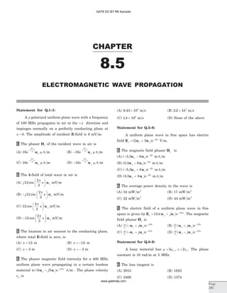
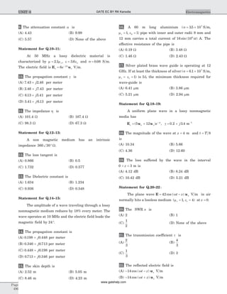
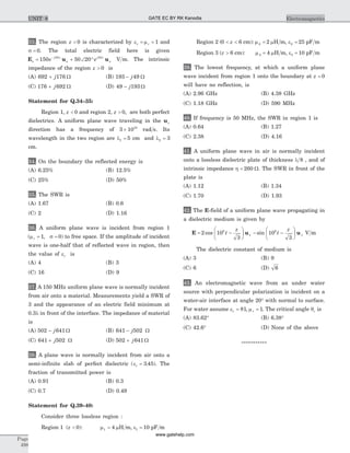
![SOLUTIONS
1. (A) w p= ´2 108
rad s
b
w p p
= =
´
´
=
c
2 10
3 10
2
3
8
8
rad m
E us
j x
ye=
-
6
2
3
p
mV m
u u uE H x´ = , u u uy H x´ = , u uH z=
H us
j x
ze=
-6
120
2
3
p
p
=
-
16
2
3
e
j x
z
p
u m A m
2. (B) For conducting plane G = -1,
E ur
j x
ye= -6
2
3
p
mV m,
E E E= +i r = -
æ
è
ç
ç
ö
ø
÷
÷
- -
6 6
2
3
2
3
e e
j x
y
j x
y
p p
u u mV m
= -
æ
è
ç
ö
ø
÷j x y12
3
sin
2p
u mV m
3. (B) The electric field vanish at the surface of the
conducting plane at x = 0. In air the first null occur at
x = - = - = -
l p
b
1
12
3
2
m
4. (C) vp = =
´ ´w
b
p2 400 10
18
6
= ´1 4 108
. m s
5. (C) The wave is propagating in forward x direction.
Therefore u u uE H x´ = .
For u uE z= , u u uz H x´ = Þ u uH y= -
For u uE y= , u u uy H x´ = Þ u uH z=
H u us y z
j x
e= - + -1
120
2 3
p
b
( ) = - + -
( . )5 3 8u uy z
j x
e b
mA m
6. (B) Pavg s s= ´
1
2
Re{ }*
E H
1
2
5 3 3 8 10 3
{( . ) ( ) }u ux x+ ´ -
= 17 3. ux mW m2
7. (D) Since Pointing vector is in the positive x
direction, therefore u u uE H x´ = .
For u uE y= , u u uy H x´ = Þ u uH z=
For u uE z= , u u uz H x´ = Þ u uH y= - ,
H u us z y
j x
j e= - -12 15
ho
( )
8. (B) Loss tangent
s
we
= x
b w
me s
we
= +
æ
è
ç
ö
ø
÷ +
é
ë
ê
ê
ù
û
ú
ú2
1 1
2
[ ]Þ =
´ ´
´
´
+ +10
2 5 10
3 10
5 2
2
1 1
6
8
2p
x
Þ = =x
s
we
1823
9. (B)
a
b
=
+ -
+ +
1 1
1 1
2
2
x
x
Þ =
a
b
1822
1824
a = ´10 0 999. = 9.99
10. (D) a w
me s
we
= +
æ
è
ç
ö
ø
÷ -
é
ë
ê
ê
ù
û
ú
ú2
1 1
2
s
we peo
=
´ ´ ´
=
0 08
3 6 50 10 2
86
.
.
a
p
=
´ ´
´
- =
2 50 10
3 10
2 1 3 6
2
65 1 5 41
6
8
( . )( . )
( ) .
b w
me s
we
= +
æ
è
ç
ö
ø
÷ +
é
ë
ê
ê
ù
û
ú
ú2
1 1
2
=
´ ´
´
+ =
2 50 10
3 10
2 1 3 6
2
65 1 6 13
6
8
p ( . )( . )
( ) .
g a b= + = +j j5 41 6 13. . per meter.
11. (A) | |h
m
e
s
we
p
=
+
æ
è
ç
ö
ø
÷
æ
è
ç
ç
ö
ø
÷
÷
= =
1
120
2 1
3 6
64
101 4
2
1
4
1
4
.
. .
12. (C)
s
we
q= = ° =tan tan .2 60 1732n
13. (D) | |h
m
e
s
we
=
+
æ
è
ç
ö
ø
÷
æ
è
ç
ç
ö
ø
÷
÷
1
2
1
4
Þ =
+
360
1 17322
1
4
120p
er
( . )
Þ =er 0 548.
Chap 8.5
Page
499
Electromagnetic Wave Propagation GATE EC BY RK Kanodia
www.gatehelp.com](https://image.slidesharecdn.com/a-150815031147-lva1-app6892/85/A-gate-by-rk-kanodia-328-320.jpg)
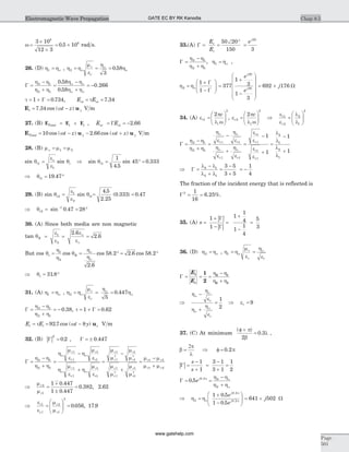
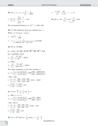
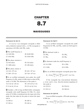
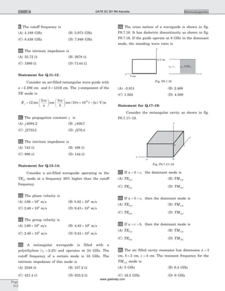
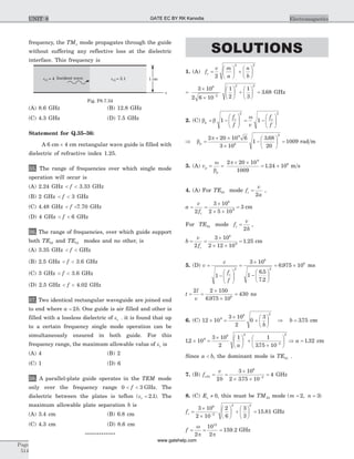
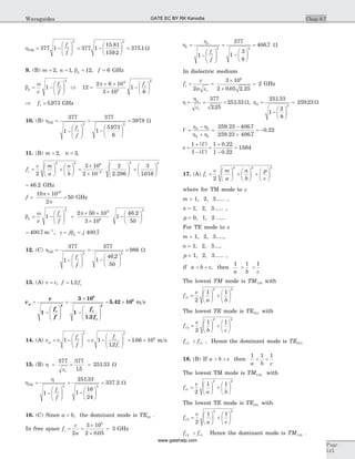

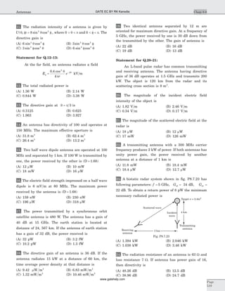
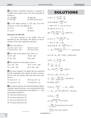
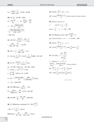
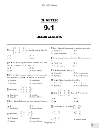
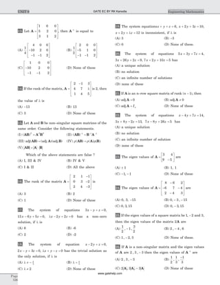
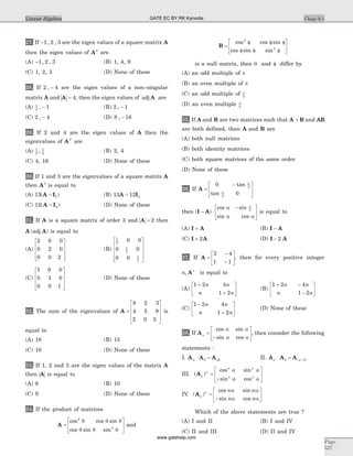
![51. If A =
é
ë
ê
ù
û
ú
t t
e tt
2
cos
sin
, then
d
dt
A
will be
(A)
t t
e tt
2
sin
sin
é
ë
ê
ù
û
ú (B)
2t t
e tt
cos
sin
é
ë
ê
ù
û
ú
(C)
2t t
e tt
-é
ë
ê
ù
û
ú
sin
cos
(D) Undefined
52. If A RÎ ´n n , det A ¹ 0, then
(A) A is non singular and the rows and columns of A
are linearly independent.
(B) A is non singular and the rows A are linearly
dependent.
(C) A is non singular and the A has one zero rows.
(D) A is singular.
************
SOLUTIONS
1. (B) A is singular if A = 0
Þ
-
-
- l
é
ë
ê
ê
ê
ù
û
ú
ú
ú
=
0 1 2
1 0 3
2 2
0
Þ - -
-
- l
½
½
½ ½
½
½+
-½
½
½ ½
½
½+
- l
½
½
½ ½
½
½=( )1
1 2
2
2
1 2
0 3
0
0 3
2
0
Þ l - + =( ) ( )4 2 3 0 Þ l - + = Þ l = -4 6 0 2
2. (C) If k is a constant and A is a square matrix of
order n n´ then k kn
A A= .
A B A B B B= Þ = = =5 5 5 6254
Þ a = 625
3. (B) A is singular, if A = 0,
A is Idempotent, if A A2
=
A is Involutory, if A2
= I
Now, A AA A A A A A A2
= = = = =( ) ( )B B B
and B BB BA B B AB BA B2
= = = = =( ) ( )
Þ =A A2
and B B2
= ,
Thus A & B both are Idempotent.
4. (B) Since, A2
5 8 0
3 5 0
1 2 1
5 8 0
3 5 0
1 2 1
=
- -
-
é
ë
ê
ê
ê
ù
û
ú
ú
ú
- -
-
é
ë
ê
ê
ê
ù
û
ú
ú
ú
=
é
ë
ê
ê
ê
ù
û
ú
ú
ú
1 0 0
0 1 0
0 0 1
= I, A I A2
= Þ is involutory.
5. (B) Let A = [ ]aij be a skew–symmetric matrix, then
A AT
= - , Þ = -a aij ij ,
if i j= then a a a aii ii ii ii= - Þ = Þ =2 0 0
Thus diagonal elements are zero.
6. (C) A is orthogonal if AA IT
=
A is unitary if AA IQ
= , where AQ
is the conjugate
transpose of A i.e., A AQ T
= ( ) .
Here,
AAQ
i
i
i
i
=
- -
é
ë
ê
ê
ê
ê
ù
û
ú
ú
ú
ú
- -
é
ë
ê
ê
ê
ê
ù
û
ú
ú
ú
ú
=
1
2 2
2
1
2
1
2 2
2
1
2
1 0
0 1
2
é
ë
ê
ù
û
ú = I
Thus A is unitary.
Chap 9.1
Page
529
Linear Algebra GATE EC BY RK Kanodia
www.gatehelp.com](https://image.slidesharecdn.com/a-150815031147-lva1-app6892/85/A-gate-by-rk-kanodia-346-320.jpg)
![7. (A) A square matrix A is said to be Hermitian if
A AQ
= . So a aij ji= . If i j= then a aii ii= i.e. conjugate of
an element is the element itself and aii is purely real.
8. (C) A square matrix A is said to be Skew-Hermitian
if A AQ
= - . If A is Skew–Hermitian then A AQ
= -
Þ = -a aji ij ,
if i j= then a aii ii= - Þ + =a aii ii 0
it is only possible when aii is purely imaginary.
9. (D) A is Hermitian then A AQ
=
Now, ( )i i i iQ Q Q
A A A A= = - = - , Þ = -( ) ( )i iQ
A A
Thus iA is Skew–Hermitian.
10. (C) A is Skew–Hermitian then A AQ
= -
Now, ( ) ( )i i iQ Q
A A A A= = - - = then iA is Hermitian.
11. (C) If A = ´[ ]aij n n then det A = ´[ ]cij n n
T
Where cij is the cofactor of aij
Also c Mij
i j
ij= - +
( )1 , where Mij is the minor of aij ,
obtained by leaving the row and the column
corresponding to aij and then take the determinant of
the remaining matrix.
Now, M11 = minor of a11 i.e. - =
-
-
½
½
½ ½
½
½= -1
1 2
2 1
3
Similarly
M12 =
2 2
2 1
-½
½
½ ½
½
½= 6 ; M13 =
-
½
½
½ ½
½
½2 1
2 2
= - 6
M21
2 2
2 1
=
- -
-
½
½
½ ½
½
½= - 6 ; M22
1 2
2 1
=
- -½
½
½ ½
½
½= 3 ;
M23
1 2
2 2
=
- -
-
½
½
½ ½
½
½= 6 ; M31
2 2
1 2
=
- -
-
½
½
½ ½
½
½= 6 ;
M32
1 2
2 2
=
- -
-
½
½
½ ½
½
½= 6 ; M33
1 2
2 1
=
- -½
½
½ ½
½
½= 3
C M11
1 1
111 3= - = -+
( ) ; C M12
1 2
121 6= - = -+
( ) ;
C M13
1 3
131 6= - = -+
( ) ; C M21
2 1
211 6= - =+
( ) ;
C M22
2 2
221 3= - =+
( ) ; C M23
2 3
231 6= - = -+
( ) ;
C M31
3 1
311 6= - =+
( ) ; C M32
3 2
321 6= - = -+
( ) ;
C M33
3 3
331 3= - =+
( )
det A =
é
ë
ê
ê
ê
ù
û
ú
ú
ú
C C C
C C C
C C C
T
11 12 13
21 22 23
31 32 33
=
- - -
-
-
é
ë
ê
ê
ê
ù
û
ú
ú
ú
=
- - -
-
-
é
ë
ê
ê
ê
ù
û
ú
3 6 6
6 3 6
6 6 3
3
1 2 2
2 1 2
2 2 1
T
ú
ú
=
T
T
3A
12. (A) Since A
A
-
=1 1
adj A
Now, Here A =
-
-
= -
1 2
3 5
1
Also, adj A =
- -
- -
é
ë
ê
ù
û
ú
5 3
2 1
T
Þ =
- -
- -
é
ë
ê
ù
û
úadj A
5 2
3 1
A-
=
-
1 1
1
- -
- -
é
ë
ê
ù
û
ú
5 2
3 1
=
é
ë
ê
ù
û
ú
5 2
3 1
13. (A) Since, A
A
A-
=1 1
adj
A = = ¹
1 0 0
5 2 0
3 1 2
4 0,
adj A ==
-
-
é
ë
ê
ê
ê
ù
û
ú
ú
ú
=
- -
é
ë
ê
ê
ê
ù
û
4 10 10
0 2 1
0 0 2
4 0 0
10 2 0
1 1 2
T
ú
ú
ú
A-
=
- -
é
ë
ê
ê
ê
ù
û
ú
ú
ú
1 1
4
4 0 0
10 2 0
1 1 2
14. (B) A matrix A( )m n´ is said to be of rank r if
(i) it has at least one non–zero minor of order r, and
(ii) all other minors of order greater than r, if any; are
zero. The rank of A is denoted by r( )A . Now, given that
r = ®( )A 2 minor of order greater than 2 i.e., 3 is zero.
Thus A =
-
l
½
½
½
½
½
½
½
½
=
2 1 3
4 7
1 4 5
0
Þ - l + - l + - =2 35 4 1 20 3 16 7 0( ) ( ) ( ) ,
Þ - l + - l + =70 8 20 27 0,
Þ l = Þ l =9 117 13
15. (A) The correct statements are
( )AB B AT T T
= , ( )AB B A- - -
=1 1 1
,
adj adj adj( ) ( ) ( )AB B A=
r ¹ r r( ) ( ) ( )AB A B , A A BB = ×
Thus statements I, II, and IV are wrong.
16. (B) Since
A = - + + - + = - + =2 9 8 2 2 3 2 2 0( ) ( )
Þ r <( )A 3
Again, one minor of order 2 is
2 1
0 3
6 0
½
½
½ ½
½
½= ¹
Þ r =( )A 2
Page
530
Engineering MathematicsUNIT 9 GATE EC BY RK Kanodia
www.gatehelp.com](https://image.slidesharecdn.com/a-150815031147-lva1-app6892/85/A-gate-by-rk-kanodia-347-320.jpg)
![37. (B) A2 3 4
1 1
3 4
1 1
5 8
2 3
=
-
-
é
ë
ê
ù
û
ú
-
-
é
ë
ê
ù
û
ú =
-
-
é
ë
ê
ù
û
ú
=
+ -
-
é
ë
ê
ù
û
ú
1 2 4
1 2
n n
n n
, where n = 2.
38. (D) A Aa b
a a
a a
b b
b b
× =
-
é
ë
ê
ù
û
ú -
é
ë
ê
ùcos sin
sin cos
cos sin
sin cos û
ú
=
+ +
- + +
é
ë
ê
ù
û
ú = +
cos ( ) sin ( )
sin ( ) cos ( )
a b a b
a b a b
a bA
Also, it is easy to prove by induction that
( )
cos sin
sin cos
Aa
a a
a a
n n n
n n
=
-
é
ë
ê
ù
û
ú
39. (A) We know that adj adj( )A A A= ×
-n 2
.
Here n = 3 and A = 3.
So, adj adj( ) ( )
A A A= × =-
3 33 2
.
40. (C) We have adj adj( )
( )
A A=
-n 1 2
Putting n = 3, we get adj adj( )A A=
4
.
41. (C) Let B A= adj adj( )2
.
Then, B is also a 3 3´ matrix.
adj adj adj adj{ ( )}A B B B2 3
3 1 2
= = =
-
= = é
ëê
ù
ûú
= =
-
adj adj( )
( )
A A A2
2
2
3 1
2
16 16
2
2
[ ]K A A2 2
=
42. (C)
2 0x
x x
é
ë
ê
ù
û
ú
1 0
1 2-
é
ë
ê
ù
û
ú =
é
ë
ê
ù
û
ú
1 0
0 1
Þ
é
ë
ê
ù
û
ú =
é
ë
ê
ù
û
ú
2 0
0 2
1 0
0 1
x
x
, So, 2 1x = Þ x =
1
2
.
43. (D) Inverse matrix is defined for square matrix only.
44. (C) AB =
-
-
é
ë
ê
ê
ê
ù
û
ú
ú
ú
- -é
ë
ê
ù
û
ú
2 1
1 0
3 4
1 2 5
3 4 0
=
+ - - + - - + -( )( ) ( )( ) ( )( ) ( )( ) ( )( ) ( )( )
( )(
2 1 1 3 2 2 1 4 2 5 1 0
1 1) ( )( ) ( )( ) ( )( ) ( )( ) ( )( )
( )( ) ( )( )
+ - + - +
- +
0 3 1 2 0 4 1 5 0 0
3 1 4 3 ( )( ) ( )( ) ( )( ) ( )( )- - + - - +
é
ë
ê
ê
ê
ù
û
ú
ú
ú3 2 4 4 3 5 4 0
=
- - -
- -
-
é
ë
ê
ê
ê
ù
û
ú
ú
ú
1 8 10
1 2 5
9 22 15
45. (C) AAT
=
-
é
ë
ê
ù
û
ú -
é
ë
ê
ê
ê
ù
û
ú
ú
ú
1 2 0
3 1 4
1 3
2 1
0 4
=
+ + + - +
+
( )( ) ( )( ) ( )( ) ( )( ) ( )( ) ( )( )
( )( ) (
1 1 2 2 0 0 1 3 2 1 0 4
3 1 - + + - - +
é
ë
ê
ù
û
ú1 2 4 0 3 3 1 1 4 4)( ) ( )( ) ( )( ) ( )( ) ( )( )
=
é
ë
ê
ù
û
ú
5 1
1 26
46. (B) if A is zero, A-1
does not exist and the matrix A
is said to be singular. Only (B) satisfy this condition.
A = = - =
5 2
2 1
5 1 2 2 1( )( ) ( )( )
47. (A) A skew symmetric matrix An n´ is a matrix with
A AT
= - . The matrix of (A) satisfy this condition.
48. (C) AB =
é
ë
ê
ù
û
ú
é
ë
ê
ê
ê
ù
û
ú
ú
ú
1 1 0
1 0 1
1
0
1
=
+ +
+ +
é
ë
ê
ù
û
ú =
( )( ) ( )( ) ( )( )
( )( ) ( )( ) ( )( )
1 1 1 0 0 1
1 1 0 0 1 1
1
2
é
ë
ê
ù
û
ú
49. (C) For orthogonal matrix
det M = 1 And M M-
=1 T
, therefore Hence D D-
=1 T
D DT A C
B BC
B
C A
=
é
ë
ê
ù
û
ú = =
-
-
-
é
ë
ê
ù
û
ú
-
0
1 01
This implies B
C
BC
=
-
-
Þ = Þ = ±B
B
B
1
1
Hence B = 1
50. (B) From linear algebra for An n´ triangular matrix
det A =
=
Õaii
i
n
1
, The product of the diagonal entries of A
51. (C )
d
dt
d t
dt
d t
dt
d e
dt
d t
dt
t
t
A
=
é
ë
ê
ê
ê
ù
û
ú
ú
ú
=
( ) (cos )
( ) (sin )
2
2 -é
ë
ê
ù
û
ú
sin
cos
t
e tt
52. (A) If det A ¹ 0, then An n´ is non-singular, but if
An n´ is non-singular, then no row can be expressed as a
linear combination of any other. Otherwise det A = 0
************
Chap 9.1
Page
533
Linear Algebra GATE EC BY RK Kanodia
www.gatehelp.com](https://image.slidesharecdn.com/a-150815031147-lva1-app6892/85/A-gate-by-rk-kanodia-349-320.jpg)
![1. If f x x x x( ) = - + -3 2
6 11 6 is on [1, 3], then the point
c « ] , [1 3 such that f c¢ =( ) 0 is given by
(A) c = ±2
1
2
(B) c = ±2
1
3
(C) c = ±2
1
2
(D) None of these
2. Let f x x( ) sin= 2 , 0 2
£ £x p
and f c¢ =( ) 0 for c « ] , [0 2
p
.
Then, c is equal to
(A)
p
4
(B)
p
3
(C)
p
6
(D) None
3. Let f x x x e
x
( ) ( )= +
-
3 2
, - £ £3 0x . Let c « -] , [3 0 such
that f c¢ =( ) 0. Then, the value of c is
(A) 3 (B) -3
(C) -2 (D) -
1
2
4. If Rolle’s theorem holds for f x x x kx( ) = - + +3 2
6 5 on
[1, 3] with c = +2
1
3
, the value of k is
(A) -3 (B) 3
(C) 7 (D) 11
5. A point on the parabola y x= -( )3 2
, where the
tangent is parallel to the chord joining A (3, 0) and B (4,
1) is
(A) (7, 1) (B)
3
2
1
4
,
æ
è
ç
ö
ø
÷
(C)
7
2
1
4
,
æ
è
ç
ö
ø
÷ (D) -
æ
è
ç
ö
ø
÷
1
2
1
2
,
6. A point on the curve y x= - 2 on [2, 3], where the
tangent is parallel to the chord joining the end points of
the curve is
(A)
9
4
1
2
,
æ
è
ç
ö
ø
÷ (B)
7
2
1
4
,
æ
è
ç
ö
ø
÷
(C)
7
4
1
2
,
æ
è
ç
ö
ø
÷ (D)
9
2
1
4
,
æ
è
ç
ö
ø
÷
7. Let f x x x x( ) ( )( )= - -1 2 be defined in [ , ]0 1
2
. Then, the
value of c of the mean value theorem is
(A) 0.16 (B) 0.20
(C) 0.24 (D) None
8. Let f x x( ) = -2
4 be defined in [2, 4]. Then, the value
of c of the mean value theorem is
(A) - 6 (B) 6
(C) 3 (D) 2 3
9. Let f x ex
( ) = in [0, 1]. Then, the value of c of the
mean-value theorem is
(A) 0.5 (B) ( )e - 1
(C) log ( )e - 1 (D) None
10. At what point on the curve y x= -(cos )1 in ] ,0 2p[ ,
is the tangent parallel to x –axis ?
(A)
p
2
1, -
æ
è
ç
ö
ø
÷ (B) ( , )p - 2
(C)
2
3
3
2
p
,
-æ
è
ç
ö
ø
÷ (D) None of these
CHAPTER
9.2
DIFFERENTIAL CALCULUS
Page
534
GATE EC BY RK Kanodia
www.gatehelp.com](https://image.slidesharecdn.com/a-150815031147-lva1-app6892/85/A-gate-by-rk-kanodia-350-320.jpg)
![11. log sin ( )x h+ when expanded in Taylor’s series, is
equal to
(A) log sin cotx h x h x+ - +
1
2
2 2
cosec K
(B) log sin cotx h x h x+ + +
1
2
2 2
sec K
(C) log sin cotx h x h x- + +
1
2
2 2
cosec K
(D) None of these
12. sin x when expanded in powers of x -
æ
è
ç
ö
ø
÷
p
2
is
(A) 1
2
2
2
3
2
4
2 3 2
+
-
æ
è
ç
ö
ø
÷
+
-
æ
è
ç
ö
ø
÷
+
-
æ
è
ç
ö
ø
÷
+
x x x
p p p
! ! !
K
(B) 1
2
2
2
4
2 2
-
-
æ
è
ç
ö
ø
÷
+
-
æ
è
ç
ö
ø
÷
-
x x
p p
! !
K
(C) x
x x
-
æ
è
ç
ö
ø
÷ +
-
æ
è
ç
ö
ø
÷
+
-
æ
è
ç
ö
ø
÷
+
p
p p
2
2
3
2
5
2
3 5
! !
K
(D) None of these
13. tan
p
4
+
æ
è
ç
ö
ø
÷x when expanded in Taylor’s series, gives
(A) 1
4
3
2 3
+ + + +x x x K
(B) 1 2 2
8
3
2 3
+ + + +x x x ...
(C) 1
2 4
2 4
+ + +
x x
! !
K
(D) None of these
14. If u exyz
= , then
¶ ¶ 
3
u
x y z
is equal to
(A) e xyz x y zxyz
[ ]1 3 2 2 2
+ +
(B) e xyz x y zxyz
[ ]1 3 3 3
+ +
(C) e xyz x y zxyz
[ ]1 3 2 2 2
+ +
(D) e xyz x y zxyz
[ ]1 3 3 3 3
+ +
15. If z f x ay x ay= + + f -( ) ( ), then
(A)
=
2
2
2
2
2
z
x
a
z
y
(B)
=
2
2
2
2
2
z
y
a
z
x
(C)
= -
2
2 2
2
2
1z
y a
z
x
(D)
= -
2
2
2
2
2
z
x
a
z
y
16. If u
x y
x y
=
+
+
æ
è
ç
ç
ö
ø
÷
÷
-
tan 1
, then x
u
x
y
u
y
+
equals
(A) 2 2cos u (B)
1
4
2sin u
(C)
1
4
tan u (D) 2 2tan u
17. If u
x y x y xy
x xy y
=
+ + -
- +
-
tan 1
3 3 2 2
2 2
, then the value of
x
u
x
y
u
y
+
is
(A)
1
2
2sin u (B) sin 2u
(C) sin u (D) 0
18. If u
y
x
x
y
x
= f
æ
è
ç
ö
ø
÷ + y
æ
è
ç
ö
ø
÷, then the value of
x
u
dx
xy
u
dx dy
y
u
y
2
2
2
2
2
2
2
2
+
+
, is
(A) 0 (B) u
(C) 2u (D) -u
19. If z e y x tx
e= =sin , log and y t= 2
, then
dz
dt
is given
by the expression
(A)
e
t
y t y
x
(sin cos )- 2 2
(B)
e
t
y t y
x
(sin cos )+ 2 2
(C)
e
t
y t y
x
(cos sin )+ 2 2
(D)
e
t
y t y
x
(cos sin )- 2 2
20. If z z u v u x xy y v a= = - - =( , ) , ,2 2
2 , then
(A) ( ) ( )x y
z
x
x y
z
y
+
= -
(B) ( ) ( )x y
z
x
x y
z
y
-
= +
(C) ( ) ( )x y
z
x
y x
z
y
+
= -
(D) ( ) ( )y x
z
x
x y
z
y
-
= +
21. If f x y y z( , ) , ( , )= f =0 0, then
(A)
×
¶f
=
×
¶f
×
f
y z
f
x y
dz
dx
(B)
×
¶f
×
=
×
f
y z
f
x
f
x
dz
dx
(C)
×
¶f
× =
×
¶f
f
y z
dz
dx
f
x y
(D) None of these
22. If z x y= +2 2
and x y axy a3 3 2
3 5+ + = , then at
x a y a
dz
dx
= =, , is equal to
(A) 2a (B) 0
(C) 2 2
a (D) a3
Chap 9.2
Page
535
Differential Calculus GATE EC BY RK Kanodia
www.gatehelp.com](https://image.slidesharecdn.com/a-150815031147-lva1-app6892/85/A-gate-by-rk-kanodia-351-320.jpg)
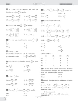
![(B) Both A and R are true and R is not a correct
explanation of A
(C) A is true but R is false
(D) A is false but R is true
34. If u x xy= log , where x y xy3 3
3 1+ + = , then
du
dx
is
equal to
(A) ( log )1
2
2
+ -
+
+
æ
è
çç
ö
ø
÷÷xy
x
y
x y
y x
(B) ( log )1
2
2
+ -
+
+
æ
è
çç
ö
ø
÷÷xy
y
x
y x
x y
(C) ( log )1
2
2
- -
+
+
æ
è
çç
ö
ø
÷÷xy
x
y
x y
y x
(D) ( log )1
2
2
- -
+
+
æ
è
çç
ö
ø
÷÷xy
y
x
y x
x y
35. If z xyf
y
x
=
æ
è
ç
ö
ø
÷, then x
z
x
y
z
y
+
is equal to
(A) z (B) 2z
(C) xz (D) yz
36. f x x x x( ) = - + +2 15 36 13 2
is increasing in the
interval
(A) ] 2, 3 [ (B) ] -¥, 3 [
(C) ] -¥, 2 [È ] 3, ¥ (D) None of these
37. f x
x
x
( )
( )
=
+2
1
is increasing in the interval
(A) ] -¥, - 1 [ È ] 1, ¥ [ (B) ] -1, 1 [
(C) ] -1, ¥ [ (D) None of these
38. f x x x( ) = -4 2
2 is decreasing in the interval
(A) ] -¥, -1 [ È ] 0, 1 [ (B) ] -1, 1 [
(C) ] -¥, -1 [ È ] 1, ¥ [ (D) None of these
39. f x x x( ) = + +9 7
3 6 is increasing for
(A) all positive real values of x
(B) all negative real values of x
(C) all non-zero real values of x
(D) None of these
40. If f x kx x x( ) = - + +3 2
9 9 3 is increasing in each
interval, then
(A) k < 3 (B) k £ 3
(C) k > 3 (D) k ³ 3
41. If a < 0, then f x e eax ax
( ) = + -
is decreasing for
(A) x > 0 (B) x < 0
(C) x > 1 (D) x < 1
42. f x x e x
( ) = -2
is increasing in the interval
(A) ] -¥ ¥, [ (B) ] -2, 0 [
(C) ] 2, ¥ [ (D) ] 0, 2 [
43. The least value of a for which f x x ax( ) = + +2
1 is
increasing on ] 1, 2, [ is
(A) 2 (B) -2
(C) 1 (D) -1
44. The minimum distance from the point (4, 2) to the
parabola y x2
8= , is
(A) 2 (B) 2 2
(C) 2 (D) 3 2
45. The co-ordinates of the point on the parabola
y x x= + +2
7 2 which is closest to the straight line
y x= -3 3, are
(A) (-2, -8) (B) (2, -8)
(C) (-2, 0) (D) None of these
46. The shortest distance of the point (0, c), where
0 5£ <c , from the parabola y x= 2
is
(A) 4 1c + (B)
4 1
2
c +
(C)
4 1
2
c -
(D) None of these
47. The maximum value of
1
x
x
æ
è
ç
ö
ø
÷ is
(A) e (B) e e
-
1
(C)
1
e
e
æ
è
ç
ö
ø
÷ (D) None of these
48. The minimum value of x
x
2 250
+
æ
è
ç
ö
ø
÷ is
(A) 75 (B) 50
(C) 25 (D) 0
49. The maximum value of f x x x( ) ( cos )sin= +1 is
(A) 3 (B) 3 3
(C) 4 (D)
3 3
4
Chap 9.2
Page
537
Differential Calculus GATE EC BY RK Kanodia
www.gatehelp.com](https://image.slidesharecdn.com/a-150815031147-lva1-app6892/85/A-gate-by-rk-kanodia-353-320.jpg)
![50. The greatest value of
f x
x
x
( )
sin
sin
=
+
æ
è
ç
ö
ø
÷
2
4
p
on the interval [ , ]0 2
p
is
(A)
1
2
(B) 2
(C) 1 (D) - 2
51. If y a x bx x= + +log 2
has its extremum values at
x = -1 and x = 2, then
(A) a b= - =
1
2
2, (B) a b= = -2 1,
(C) a b= = -2
1
2
, (D) None of these
52. The co-ordinates of the point on the curve
4 5 202 2
x y+ = that is farthest from the point (0, -2) are
(A) ( , )5 0 (B) ( , )6 0
(C) (0, 2) (D) None of these
53. For what value of x x0
2
£ £
æ
è
ç
ö
ø
÷
p
, the function
y
x
x
=
+( tan )1
has a maxima ?
(A) tan x (B) 0
(C) cot x (D) cos x
*************
SOLUTIONS
1. (B) A polynomial function is continuous as well as
differentiable. So, the given function is continuous and
differentiable.
f( )1 0= and f( )3 0= . So, f f( ) ( )1 3= .
By Rolle’s theorem Ec such that ¢ =f c( ) 0.
Now, f x x x¢ = - +( ) 3 12 112
Þ ¢ = - +f c c c( ) 3 12 112
.
Now, f c c c¢ = Þ - + =( ) 0 3 12 11 02
Þ = ±
æ
è
ç
ö
ø
÷c 2
1
3
.
2. (A) Since the sine function is continuous at each
x R« , so f x x( ) sin= 2 is continuous in 0
2
,
pé
ëê
ù
ûú.
Also, f x x¢ =( ) cos2 2 , which clearly exists for all
x « ] , [0
2
p
.So, f x( ) is differentiable in x « ] , [0
2
p
.
Also, f f( )0
2
0=
æ
è
ç
ö
ø
÷ =
p
. By Rolle’s theorem, there exists
c « ] , [0
2
p
such that ¢ =f c( ) 0.
2 2 0cos c = Þ 2
2
c =
p
Þ c =
p
4
.
3. (C) Since a polynomial function as well as an
exponential function is continuous and the product of
two continuous functions is continuous, so f x( ) is
continuous in [-3, 0].
f x x e e x x e
x x
x x x
¢ = + × - + =
+ -é
ë
ê
ù
û
ú
- - -
( ) ( ) ( )2 3
1
2
3
6
2
2 2 2 2
2
which clearly exists for all x « -] , [3 0 .
f x( ) is differentiable in ] -3, 0 [.
Also, f f( ) ( )- = =3 0 0.
By Rolle’s theorem c « -] 3, 0 [ such that f c¢ =( ) 0.
Now, f c¢ =( ) 0 Þ e
c c
c
- + -é
ë
ê
ù
û
ú =2
2
6
2
0
c c+ - =6 02
i.e. c c2
6 0- - =
Þ ( ) ( )c c+ - =2 3 0 Þ c c= - =2 3, .
Hence, c = -2 « ] -3, 0 [ .
4. (D) f x c x k¢ = - +( ) 3 122
f c c c k¢ = Þ - + =( ) 0 3 12 02
Page
538
Engineering MathematicsUNIT 9 GATE EC BY RK Kanodia
www.gatehelp.com](https://image.slidesharecdn.com/a-150815031147-lva1-app6892/85/A-gate-by-rk-kanodia-354-320.jpg)
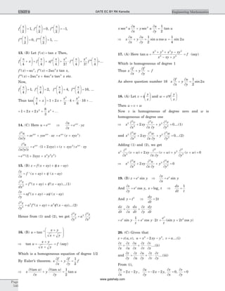
![Substituting these values in (ii) and (iii)
=
- +
×
z
x
z
u
x y
z
v
( )2 2 0....(iv)
and
=
× - - +
×
z
y
z
u
x y
z
v
( )2 2 0....(v)
From (iv) and (v), we get
( ) ( )x y
z
x
y x
z
y
+
= -
21. (C) Given that f x y y z( , ) , ( , )= f =0 0
These are implicit functions
dy
dx
f
x
f
y
dz
dy
y
z
= -
= -
¶f
¶f
,
dy
dx
dz
dy
f
x
f
y
y
z
× =
-
æ
è
ç
ç
ç
ç
ö
ø
÷
÷
÷
÷
´
-
¶f
¶f
æ
è
ç
ç
ç
ç
ö
ø
÷
÷
÷
÷
or,
×
¶f
× =
×
¶f
f
y z
dz
dx
f
x y
22. (B) Given that z x y= +2 2
and x y axy a3 3 2
3 5+ + = ...(i)
dz
dx
z
x
z
y
dy
dx
=
+
× ....(ii)
from (i),
=
+
×
z
x x y
x
1
2
2
2 2
,
=
+
×
z
y x y
y
1
2
2
2 2
and 3 3 3 3 1 02 2
x y
dy
dx
ax
dy
dx
ay+ + + =.
Þ = -
+
+
æ
è
çç
ö
ø
÷÷
dy
dx
x ay
y ax
2
2
Substituting these value in (ii), we get
dz
dx
x
x y
y
x y
x ay
y ax
=
+
+
+
-
+
+
æ
è
çç
ö
ø
÷÷2 2 2 2
2
2
dz
dx
a
a a
a
a a
a aa
a a aa a
æ
è
ç
ö
ø
÷ =
+
+
+
-
+
+
æ
è
çç
ö
ø
÷÷ =
( , ) .2 2 2 2
2
2
0
23. (B) Given that x r= cos q, y r= sin q....(i)
dx
dt
x
r
dr
dt
x d
dt
=
× +
×
q
q
....(ii)
From (i),
=
x
r
cos q,
= -
x
r
q
qsin
Substituting these values in (ii), we get
dx
dt
dr
dt
r
d
dt
= - ×cos sinq q
q
24. (C) r x y2 2 2
= + Þ
=
r
x
x2 and
=
r
y
y2
and
=
2
2
2
r
x
and
=
2
2
2
r
y
Þ
+
= + +
2
2
2
2
2 2 4
r
x
r
y
and
æ
è
ç
ö
ø
÷ +
æ
è
çç
ö
ø
÷÷ = + =
r
x
r
y
x y r
2 2
2 2 2
4 4 4
Þ
+
=
2
2
2
2 2
1r
x
y
y r
æ
è
ç
ö
ø
÷ +
æ
è
çç
ö
ø
÷÷
ì
í
ï
îï
ü
ý
ï
þï
r
x
r
y
2 2
25. (A) x r y r= =cos , sinq q
Þ =tan q
y
x
Þ =
æ
è
ç
ö
ø
÷
-
q tan 1 y
x
Þ
=
+
-æ
è
ç
ö
ø
÷ =
-
+
q
x y x
y
x
y
x y
1
1 2 2 2 2
( )
and
=
-
+
2
2 2 2 2
2q
x
xy
x y( )
Similarly
=
+
2
2 2 2 2
2q
y
xy
x y( )
and
+
=
2
2
2
2
0
q q
x y
26. (D) Given that u x ym n
=
Taking logarithm of both sides, we get
log log logu m x n y= +
Differentiating with respect to x, we get
1 1 1
u
du
dx
m
x
n
y
dy
dx
= × + × or,
du
u
m
dx
x
n
dy
y
= + ×
27. (D) Given that f x y y ax x( , ) = - + =3 2 3
3 0
f ax x f y f a xx y xx= - + = = - +6 3 3 6 62 2
, , ,
f y fyy xy= =6 0,
d y
dx
f f f f f f f
f
xx y x y xy yy x
y
2
2
2 2
3
2
= -
- +é
ë
ê
ù
û
ú
( ) ( )
( )
= -
- - + -é
ë
ê
ù
û
ú
( ( ) ( )
( )
6 6 3 0 6 3 6
3
2 2 2 2
2 3
x a y y x ax
y
= - - - +
2
45
3 3 2 2
y
ax ay a x( )
= - - + +
2
45
3 3 2 2
y
a a y a x[ ( ) ]
= - - +
2
3 45
2 2 2
y
a ax a x[ ( ) ] [ x y ax3 3 2
3 0+ - = ]
= -
2 2 2
5
a x
y
28. (A) Given that z
y
x
= -
tan 1
....(i)
Chap 9.2
Page
541
Differential Calculus GATE EC BY RK Kanodia
www.gatehelp.com](https://image.slidesharecdn.com/a-150815031147-lva1-app6892/85/A-gate-by-rk-kanodia-356-320.jpg)
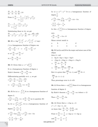
![From (ii), we get
3 3 3 1 02 2
x y
dy
dx
x
dy
dx
y+ + + ×
æ
è
ç
ö
ø
÷ = Þ = -
+
+
æ
è
çç
ö
ø
÷÷
dy
dx
x y
y x
2
2
Substituting these in (A), we get
du
dx
xy
x
y
x y
y x
= + + -
+
+
æ
è
çç
ö
ø
÷÷
ì
í
î
ü
ý
þ
( log )1
2
2
35. (B) The given function is homogeneous of degree 2.
Euler’s theorem x
z
x
y
z
y
z
+
= 2
36. (C) ¢ = - + = - -f x x x x x( ) ( )( )6 30 36 6 2 32
Clearly, ¢ >f x( ) 0 when x < 2 and also when x > 3.
f x( ) is increasing in ] -¥, 2 [ È ] 3, ¥ [.
37. (B) f x
x x
x
x
x
¢ =
+ -
+
=
-
+
( )
( )
( ) ( )
2 2
2 2
2
2 2
1 2
1
1
1
Clearly, ( )x2 2
1 0+ > for all x.
So, f x¢ >( ) 0 Þ - >( )1 02
x
Þ ( ) ( )1 1 0- + >x x
This happens when - < <1 1x .
So, f x( ) is increasing in ] -1, 1 [.
38. (A) f x x x x x x¢ = - = - +( ) ( )( )4 4 4 1 13
.
Clearly, f x¢ <( ) 0 when x < - 1 and also when x > 1.
Sol. f x( ) is decreasing in ] -¥, -1 [ È ] 1, ¥ [.
39.(C) f x x x¢ = + >( ) 9 21 08 6
for all non-zero real values
of x.
40. (C) f x kx x kx x¢ = - + = - +( ) [ ]3 18 9 3 6 32 2
This is positive when k > 0 and 36 12 0- <k or k > 3.
41. (A) f x e e axax ax
( ) ( ) cosh= + =-
2 .
¢ = <f x a ax( ) sinh2 0 When x > 0 because a < 0
42. (D) ¢ = - + = -- - -
f x x e xe e x xx x x
( ) ( )2
2 2 .
Clearly, ¢ >f x( ) 0 when x > 0 and x < 2.
43. (B) ¢ = +f x x a( ) ( )2
1 2 2 2 4< < Þ < <x x Þ + < + < +2 2 4a x a a
Þ + < ¢ < +( ) ( ) ( )2 4a f x a .
For f x( ) increasing, we have ¢ >f x( ) 0.
2 0+ ³a or a ³ - 2. So, least value of a is -2.
44. (B) Let the point closest to (4, 2) be ( , )2 42
t .
Now, D t t= - + -( ) ( )2 4 4 22 2 2
is minimum when
E t t= - + -( ) ( )2 4 4 22 2 2
is minimum.
Now, E t t= - +4 16 204
Þ = - = - + +
dE
dt
t t t t16 16 16 1 13 2
( ) ( )
dE
dt
t= Þ =0 1
d E
dt
t
2
2
2
48= . So,
d E
dt t
2
2
1
48 0
é
ë
ê
ù
û
ú = >
=( )
.
So, t = 1 is a point of minima.
Thus Minimum distance = - + - =( ) ( )2 4 4 2 2 22 2
.
45. (A) Let the required point be P x y( , ). Then,
perpendicular distance of P x y( , ) from y x- + =3 3 0 is
p
y x x x x
=
- +
=
+ + - +3 3
10
7 2 3 3
10
2
=
+ +
=
+ +x x x2 2
4 5
10
2 1
10
( )
or p
x
=
+ +( )2 1
10
2
So,
dp
dx
x
=
+2 2
10
( )
and
d p
dx
2
2
2
10
=
dp
dx
= 0 Þ x = -2, Also,
d p
dx x
2
2
2
0
æ
è
çç
ö
ø
÷÷ >
=-
.
So, x = -2 is a point of minima.
When x = -2, we get y = - + ´ - + = -( ) ( )2 7 2 2 82
.
The required point is ( , )- -2 8 .
46. (C) Let A c( , )0 be the given point and P x y( , ) be any
point on y x= 2
.
D x y c= + -2 2
( ) is shortest when E x y c= + -2 2
( ) is
shortest.
Now,
E x y c y y c= + - = + -2 2 2
( ) ( ) Þ E y y cy c= + - +2 2
2
dE
dy
y c= + -2 1 2 and
d E
dy
2
2
2 0= > .
dE
dy
= 0 Þ y c= -
æ
è
ç
ö
ø
÷
1
2
Thus E minimum, when y c= -
æ
è
ç
ö
ø
÷
1
2
Also, D c c c= -
æ
è
ç
ö
ø
÷ + - -
æ
è
ç
ö
ø
÷
1
2
1
2
2
... x y c2 1
2
= = -
æ
è
ç
ö
ø
÷
é
ë
ê
ù
û
ú
= - =
-
c
c1
4
4 1
2
Chap 9.2
Page
543
Differential Calculus GATE EC BY RK Kanodia
www.gatehelp.com](https://image.slidesharecdn.com/a-150815031147-lva1-app6892/85/A-gate-by-rk-kanodia-358-320.jpg)
![47. (B) Let y
x
x
=
æ
è
ç
ö
ø
÷
1
then, y x x
= -
Þ = - +-dy
dx
x xx
( log )1
d y
dx
x x x
x
x x
2
2
2
1
1
= + - ×- -
( log )
dy
dx
= 0 Þ 1 0+ =log x Þ x
e
=
1
d y
dx ex
e
e
2
2
1
1
1
1
0
é
ë
ê
ù
û
ú = -
æ
è
ç
ö
ø
÷ <
=
æ
è
çç
ö
ø
÷÷
- -
.
So, x
e
=
1
is a point of maxima. Maximum value = e e1
.
48. (A) ¢ = -f x x
x
( ) 2
250
2
and ¢¢ = +
æ
è
ç
ö
ø
÷f x
x
( ) 2
500
3
¢ =f x( ) 0 Þ 2
250
02
x
x
- = Þ x = 5.
¢¢ = >f ( )5 6 0. So, x = 5 is a point of minima.
Thus minimum value = +
æ
è
ç
ö
ø
÷ =25
250
5
75.
49. (D) ¢ = - +f x x x( ) ( cos )(cos )2 1 1 and
¢¢ = - +f x x x( ) sin ( cos )1 4 .
¢ =f x( ) 0 Þ =cos x
1
2
or cos x = -1 Þ =x p 3 or
x = p.
¢¢æ
è
ç
ö
ø
÷ =
-
<f
p
3
3 3
2
0. So, x = p 3 is a point of maxima.
Maximum value =
æ
è
ç
ö
ø
÷ +
æ
è
ç
ö
ø
÷ =sin cos
p p
3
1
3
3 3
4
.
50. (C) f x
x x
x x
( )
sin cos
sin cos
=
+
2
2
=
+
=
2 2 2 2
( )sec cosecx x z
(say),
where z x x= +( )sec cosec .
dz
dx
x x x x
x
x
x= - = -sec cosectan cot
cos
sin
(tan )2
3
1 .
dz
dx
= 0 Þ tan x = 1 Þ x =
p
4
in 0
2
,
pé
ëê
ù
ûú.
Sign of
dz
dx
changes from -ve to +ve when x passes
through the point p 4. So, z is minimum at x = p 4 and
therefore, f x( ) is maximum at x = p 4.
Maximum value =
+
=
2 2
4 4
1
[sec( ) ( )]p pcosec
.
51. (C)
dy
dx
a
x
bx= + +2 1
dy
dx x
é
ëê
ù
ûú =
=-( )1
0 Þ - - + =a b2 1 0 Þ + =a b2 1....(i)
dy
dx x
é
ëê
ù
ûú =
=( )2
0 Þ + + =
a
b
2
4 1 0
Þ + = -a b8 2....(ii)
Solving (i) and (ii) we get b = -
1
2
and a = 2.
52. (C) The given curve is
x y2 2
5 4
1+ = which is an
ellipse.
Let the required point be ( cos , sin )5 2f f . Then,
D = f - + f +( cos ) ( sin )5 0 2 22 2
is maximum
when z D= 2
is maximum
z = f + + f5 4 12 2
cos ( sin )
Þ
f
= - f f + + f f
dz
d
10 8 1cos sin ( sin )cos
dz
df
= 0 Þ 2 4 0cos ( sin )f - f =
Þ f =cos 0 Þ f =
p
2
.
dz
df
= - f + fsin cos2 8 Þ
f
= - f - f
d z
d
2
2
2 2 8cos sin
when f =
p
2
,
d z
d
2
2
0
f
< .
z is maximum when f =
p
2
. So, the required point is
5
2 2
cos , sin
p pæ
è
ç
ö
ø
÷ i.e. (0, 2).
53. (D) Let z
x
x x
x
x
=
+
= +
1 1tan tan
Then,
dz
dx x
x= - +
1
2
2
sec and
d z
dx x
x x
2
2 3
22
2= + sec tan
dz
dx
= 0 Þ - + =
1
02
2
x
xsec Þ x x= cos .
d z
dx
x x x
x x
2
2
3 2
2 2 0
é
ë
ê
ù
û
ú = + >
=cos
cos tansec .
Thus z has a minima and therefore y has a maxima at
x x= cos .
************
Page
544
Engineering MathematicsUNIT 9 GATE EC BY RK Kanodia
www.gatehelp.com](https://image.slidesharecdn.com/a-150815031147-lva1-app6892/85/A-gate-by-rk-kanodia-359-320.jpg)

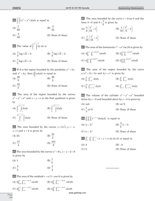
![SOLUTIONS
1. (A)
x
x
dx2
1+ò
Put x t2
1+ = Þ 2 xdx dt=
x
x
dx
t
dt2
1
1
2
1
+
= ×ò ò
=
1
2
log t = +
1
2
12
log ( )x
2. (A) F x a dx Kx
( ) = +ò = +
a
a
K
x
log
Þ = +F a
a
a
K
a
( )
log
K
a
a
a
a
a
a a
= - =
-1 1
log log log
F x
a
a
a
a
x a
( )
log log
= +
-1
= - +
1
1
log
[ ]
a
a ax a
3. (C)
dx
x1 +ò sin
=
+
æ
è
ç
ö
ø
÷ +
ò
dx
x x x x
sin cos sin cos2 2
2 2
2
2 2
=
+
æ
è
ç
ö
ø
÷
ò
dx
x x
cos sin
2 2
2
=
+
æ
è
ç
ö
ø
÷
ò
sec2
2
2
1
2
x
x
dx
tan
Put 1
2
+ =tan
x
t
Þ =sec2
2
2
x
dx dt Þ = - +ò
2 2
2
dt
t
dt
t
K
=
-
+
+
2
1
2
tan
x
K =
-
+
+
2
2
2 2
cos
cos sin
x
x x
K
=
-
+
´
-
-
+
2
2
2 2
2 2
2 2
cos
cos sin
cos sin
cos sin
x
x x
x x
x x
K
=
- +
-
+
2
2
2
2 2
2 2
2
2 2
cos sin cos
cos sin
x x x
x x
K
=
- + +
+
( cos ) sin
cos
1 x x
x
k = - - +tan x x Ksec 1
= - +tan x x csec
4. (A) Let I
x
x x
dx=
+
- +ò
3 1
2 2 32
Let 3 1 4 2x p x q+ = - +( ) Þ p q= =
3
4
5
2
,
I
x
x x
dx=
-
- +ò
3
4
4 2
2 2 32
+
- +ò
5
2 2 2 32
dx
x x
= - +
3
4
2 2 32
log ( )x x +
-
æ
è
ç
ö
ø
÷ +
æ
è
ç
ç
ö
ø
÷
÷
ò
5
4 1
2
5
2
2 2
dx
x
= - + +
æ
è
ç
ç
ö
ø
÷
÷
-
-3
4
2 2 3
5
4
1
5
2
1
2
5
2
2 1
log ( ) tanx x
x
5. (C) Let I
dx
x
=
+ò1 3 2
sin
=
+ò
cosec
cosec
2
2
3
x dx
x
=
+ +ò
cosec2
2
1 3
x dx
x( cot )
Put cot x t x dx dt= Þ - =cosec2
I
dt
t
t x
=
-
+
= =
æ
è
ç
ö
ø
÷ò
- -
4
1
2 2
1
2 22
1 1
cot cot
cot
= -1
2
21
tan ( tan )x
6. (C) Let I
x x
x x
dx=
+
+ò
2 3
3 4
sin cos
sin cos
Let ( sin cos ) ( cos sin )2 3 3 4x x p x x+ = -
+ +q x x( sin cos )3 4
p =
1
25
, q =
18
25
I
x x
x x
dx
x x
=
-
+
+
+
ò
1
25
3 4
3 4
18
25
3 4
3
cos sin
sin cos
sin cos
sin x x
dx
+ò 4 cos
= + +
1
25
3 4
18
25
log ( sin cos )x x x
7. (B) 3 8 3 2
+ -ò x x dx =
æ
è
ç
ö
ø
÷ - -
æ
è
ç
ö
ø
÷ò3
5
3
4
3
2 2
x dx
= -
æ
è
ç
ö
ø
÷
æ
è
ç
ö
ø
÷ - -
æ
è
ç
ö
ø
÷ +
æ
è
ç
ö
ø
÷
-
3
1
2
4
3
5
3
4
3
5
3
2 2 2
1
x x sin
x -
æ
è
ç
ç
çç
ö
ø
÷
÷
÷÷
ì
í
ï
î
ï
ü
ý
ï
þ
ï
4
3
5
3
=
-
+ - +
--3 4
6
3 8 3
25 3
18
3 4
5
2 1x
x x
x
sin
8. (B)
dx
x x2 3 42
+ +
ò =
+
æ
è
ç
ö
ø
÷ +
æ
è
ç
ç
ö
ø
÷
÷
ò
1
2
3
4
23
4
2 2
dx
x
Chap 9.3
Page
549
Integral calculus GATE EC BY RK Kanodia
www.gatehelp.com](https://image.slidesharecdn.com/a-150815031147-lva1-app6892/85/A-gate-by-rk-kanodia-363-320.jpg)
![=
+
æ
è
ç
ç
ö
ø
÷
÷
-1
2
3
4
23
4
1
sinh
x
=
+-1
2
4 3
23
1
sinh
x
9. (B)
2 3
12
x
x x
dx
+
+ +
ò
=
+
+ +
+
+ +
ò ò
2 1
1
2
12 2
x
x x
dx
dx
x x
=
+
+ +
+
+
æ
è
ç
ö
ø
÷ +
æ
è
ç
ç
ö
ø
÷
÷
ò ò
2 1
1
2
1
2
3
2
2 2 2
x
x x
dx
dx
x
=
+ +
+
+
-( )
sinh
x x
x2 1 2
11
1
2
2
1
2
3
2
= + + +
+-
2 1 2
2 1
3
2 1
x x
x
sinh
10. (B)
dx
x x
I
1 -
=ò
Put x dx d= Þ =sin sin cos2
2q q q q
I d d=
-
=ò ò
2
1
2
2
sin cos
sin sin
sin cos
sin cos
q q
q q
q
q q
q q
q
I d c= = +ò2 2q q = +-
2 1
sin x c
I x c= - +-
sin ( )1
2 1
11. (D) Let I
x x x
dx=
+ - -
ò
1
1 1 2 2
( )
Put x
t
+ =1
1
Þ dx
t
dt= -
1
2
I t
dt
t t t
dt
t
=
-
- -
æ
è
ç
ö
ø
÷ - -
æ
è
ç
ö
ø
÷
= -
-
ò ò
1
1
1 2
1
1
1
1
2 1
2
2 2
= -
-
æ
è
ç
ç
ö
ø
÷
÷
ò
1
2 1
2
2
2
dt
t
= - -1
2
1
1 2
cosh
t
= -
+
æ
è
ç
ç
ö
ø
÷
÷
-1
2
2
1
1
cosh
x
12. (C)
dx
x xsin cos+ò
=
+
ò
1
2
4 4
dx
x xsin cos cos sin
p p
=
+
æ
è
ç
ö
ø
÷
ò
1
2
4
dx
xsin
p
= +
æ
è
ç
ö
ø
÷ò
1
2 4
cosec x dx
p
= - +
æ
è
ç
ö
ø
÷
é
ë
ê
ù
û
ú
1
2
1
2 4
log cot x
p
= +
æ
è
ç
ö
ø
÷
1
2 2 8
log tan
x p
13. (D)
dx
x a x bsin( )sin( )- -ò
=
-
-
- -ò
1
sin( )
sin( )
sin( ) sin( )a b
a b dx
x a x b
=
-
- - -
- -ò
1
sin( )
sin [( ) ( )]
sin( ) sin( )a b
x b x a
x a x b
dx
=
-
1
sin ( )a b
´
- - - - -
- -
sin( ) cos( ) cos( ) sin( )
sin( ) sin( )
x b x a x b x a
x a x b
dxò
=
-
- - -ò
1
sin( )
[cot( ) cot( )]
a b
x a x b dx
=
-
- - -
1
sin ( )
[log sin ( ) log sin ( )]
a b
x a x b dx
=
-
-
-
ì
í
î
ü
ý
þ
1
sin ( )
log
sin( )
sin( )a b
x a
x b
14. (D) Let I
dx
e
e dx
ex
x
x
=
-
=
-ò ò
-
-
1 1
Put 1 - =-
e tx
Þ e dx dtx-
=
I
dt
t
t e x
= = = -ò
-
log log ( )1
15. (B) Let I
dx
x x x
=
+ + +ò1 2 3
=
+ +ò
dx
x x( ) ( )1 1 2
Let
1
1 1 1 12 2
( )( )+ +
=
+
+
+
+x x
A
x
Bx C
x
1 1 12
= + + + +A x Bx C x( ) ( )( )
Comparing the coefficients of x x2
, and constant terms,
A B+ = 0, B C+ = 0, C A+ = 1
Solving these equations, we get
A =
1
2
, B C= - =
1
2
1
2
,
I
x
dx
x
x
dx=
+
-
-
+ò ò
1
2
1
1
1
2
1
12
= + - + + -1
2
1
1
2
1
1
2
2 1
log ( ) log ( ) tanx x x
=
+
+
+
é
ë
ê
ù
û
ú
-1
4
1
1
2
2
2
1
log
( )
tan
x
x
x
Page
550
Engineering MathematicsUNIT 9 GATE EC BY RK Kanodia
www.gatehelp.com](https://image.slidesharecdn.com/a-150815031147-lva1-app6892/85/A-gate-by-rk-kanodia-364-320.jpg)
![16. (B) Let I
x
x
dx=
-ò
sin
sin1
=
- -
-ò
1 1
1
( sin )
sin
x
x
dx
=
-
-ò ò
1
1 sin x
dx dx =
+
-
-ò
1
1 2
sin
sin
x
x
dx x
=
+
-ò
1
2
sin
cos
x
x
dx x = + -ò( tan )sec sec2
x x x dx x
= + -tan x x xsec
17. (B) Let I e f x f x dxx
= + ¢ò { ( ) ( )}
= + ¢ò òe f x dx e f x dxx x
( ) ( )
= - ¢ + ¢ = ×ò ò{ ( ) ( ) } ( ) ( )f x e f x e dx e f x dx f x ex x x x
18. (A) Let I e
x
x
dxx
=
+
+
æ
è
çç
ö
ø
÷÷ò
1
1
sin
cos
=
+
æ
è
ç
ç
çç
ö
ø
÷
÷
÷÷
òe
x x
x
dxx
1 2
2 2
2
2
2
sin cos
cos
= +ò ò
1
2 2 2
2
e
x
dx e
x
dxx x
sec tan
= × - ×
ì
í
î
ü
ý
þ
+ò ò
1
2
2
2
2
2 2
e
x
e
x
dx e
x
dxx x x
tan tan tan
= +e
x
cx
tan
2
19. (C) I
x
x
dx=
+ò
3
2
1
=
×
+ò
x x
x
dx
2
2
1
=
+ -
+ò
x x
x
dx
( )2
2
1 1
1
= -
+ò òxdx
x
x
dx2
1
= - + +
1
2
1
2
12 2
x x clog ( )
20. (A) Let I x dx= -
òsin 1
= × ×-
òsin 1
1x dx
= × -
-
×-
òsin 1
2
1
1
x x
x
x dx
= -
-
-
òx x
x
x
dxsin 1
2
1
In second part put 1 2 2
- =x t
xdx tdt= - = +-
òx x dtsin 1
= +-
x x tsin 1
= + - +-
x x x csin 1 2
1
21.
sin cos
sin
x x
x
dx
+
+
ò 1 2
=
+
+ +
ò
sin cos
(sin cos ) sin cos
x x
x x x x
dx
2 2
2
=
+
+
ò
sin cos
(cos cos )
x x
x x
dx
2
=
+
+
= =ò ò
sin cos
sin cos
x x
x x
dx dx x
22. (D) 5 3 5 3 5 3
0
3 5
0
3 5
3 5
1
x dx x dx x dx- = - - + -ò ò ò
= - +
æ
è
ç
ö
ø
÷ + -
æ
è
çç
ö
ø
÷÷
5
2
3
5
2
32
0
3 5 2
3 5
1
x x
x
x
= - +
æ
è
ç
ö
ø
÷ + -
æ
è
ç
ö
ø
÷ - -
æ
è
ç
ö
ø
÷
é
ë
ê
ù
û
ú
9
10
9
5
5
2
3
9
10
9
5
= + - +
æ
è
ç
ö
ø
÷ =
9
10
1
2
9
10
13
10
23. (B)
dx
e ex x
+ -ò0
1
=
+ò
e dx
e
x
x2
0
1
1
Put e tx
= Þ e dx dtx
= =
+
=ò
-dt
t
t
e
e
2
1
1
1
1
[tan ]
= -- -
tan tan1 1
1e = --
tan 1
4
e
p
24. (D) x x dx x x dx
c c
( ) ( )1
0
2
0
- = -ò ò
= -
æ
è
ç
ö
ø
÷
1
2
1
3
2 3
0
x x
c
= -
1
6
3 22
c c( )
x x dx
c
( )1 0
0
- =ò Þ
1
6
3 2 02
c c( )- =
Þ =c
3
2
25. (D) Put x x t2
+ = Þ ( )2 1x dx dt+ =
2 1
2 2 2
2
0
1
0
2
1 2
0
2x
x x
dx
dt
t
t
+
+
= = =ò ò ( )
26. (A) x xdx4 5
sin
p
p
ò
Since, f x x x( ) ( ) sin ( )- = - -4 5
= -x x4 5
sin
f x( ) is odd function thus
x x dx4 5
0sin =òp
p
27. (A) cos (cos )2
0
2
0
2
1
2
2 1x dx x dx
p p
ò ò= +
Chap 9.3
Page
551
Integral calculus GATE EC BY RK Kanodia
www.gatehelp.com](https://image.slidesharecdn.com/a-150815031147-lva1-app6892/85/A-gate-by-rk-kanodia-365-320.jpg)
![= +
æ
è
ç
ö
ø
÷
1
2
1
2
2
0
2
sin x x
p
= - + -
æ
è
ç
ö
ø
÷
é
ë
ê
ù
û
ú
1
2
1
2
0
2
0(sin sin )p
p
= - - +
é
ëê
ù
ûú =
1
2
1
2
0 0 0
2 4
( )
p p
Aliter 1. cos2
0
2
x dx
p
ò =
æ
è
ç
ö
ø
÷
æ
è
ç
ö
ø
÷
æ
è
ç
ö
ø
÷
G G
G
3
2
1
2
2
4
2
=
1
2
2
p
=
p
4
Aliter 2. Use Walli’s Rule cos2
0
2
1
2 2 4
x
p
p p
ò = × =
28. (B) Let I a x dx
a
= -ò
2 2
0
Put x a dx a d= Þ =sin cosq q q when x = 0, q = 0,
when x a= , q
p
=
2
I a a a d= -ò
2 2 2
0
2
sin cosq q q
p
= = × ×òa d a2 2
0
2
2
1
2 2
cos q q
p
p
(By Walli’s Formula)
=
pa2
4
Aliter: a x dx
a
2 2
0
-ò
= - +
é
ëê
ù
ûú
-1
2
1
2
2 2 2 1
0
x a x a
x
a
a
sin = +
é
ë
ê
ù
û
ú0
4
2
pa
=
pa2
4
29. (D) Let I x dx= òlog (tan )
0
2p
....(1)
I x dx= -
æ
è
ç
ö
ø
÷òlog tan
p
p
20
2
I x= òlog (cot )
0
2p
....(2)
Adding (1) and (2), we get
2
0
2
I x x dx= +ò[log (tan ) log (cot )]
p
= ×òlog (tan cot )x x dx
0
2p
= =òlog 1 0
0
2
dx
p
Þ I = 0
30. (D) Let I
t
dt= -
æ
è
ç
ö
ø
÷ò2
2 40
1
sin
p p
....(i)
= - -
æ
è
ç
ö
ø
÷ò2
2
1
40
1
sin ( )
p p
t dt = -
æ
è
ç
ö
ø
÷ò2
4 20
1
sin
p p
t dt
= - -
æ
è
ç
ö
ø
÷ = -ò2
2 4
1
0
1
sin
p p
t dt
2 0 0I I= Þ =
31. (C) Let I
f x
f x f a x
dx
a
=
+ -ò
( )
( ) ( )20
2
....(1)
I
f a x
f a x f x
dx
a
=
-
- +ò
( )
( ) ( )
2
20
2
....(2)
Adding (1) and (2), we get
2
2
20
2
I
f x f a x
f x f a x
dx
a
=
+ -
+ -ò
( ) ( )
( ) ( )
= × = =ò1 2
0
2
0
2
dx x a
a
a
[ ]
Þ =I a
32. (C) Let I
e
x
xdx
x
=
-
-
ò
1
2
0
1 2
1
Put 1 2
- =x t
Þ
-
- =
1
2 1
2
2
x
x dx dt( )
when x t= =0 1, , when x t= =1 0,
I e dt e e e et t
= - = - = - - = -ò1
0
1
0 0 1
1[ ] [ ]
33. (B) Let I
dx
x x
=
- +ò1 2
0
1
=
-
æ
è
ç
ö
ø
÷ +
æ
è
ç
ç
ö
ø
÷
÷
ò
dx
x
1
2
3
2
2 2
0
1
=
-
é
ë
ê
ê
ê
ê
ù
û
ú
ú
ú
ú
-1
3
2
1
2
3
2
1
0
1
tan
x
= - -
æ
è
ç
ç
ö
ø
÷
÷
é
ë
ê
ù
û
ú
- -2
3
1
3
1
3
1 1
tan tan = +
æ
è
ç
ö
ø
÷
2
3 6 6
p p
= =
2
3 3
2 3
9
p p
34. (B) Let I
x
x
dx=
-
ò1
1
=
-
+
-
ò ò
x
x
dx
x
x
dx
1
0
0
1
= - + ×
-
ò ò1 1
1
0
0
1
dx dx = - +-[ ] [ ]x x1
0
0
1
= - - - + - =[ ( )] [ ]0 1 1 0 0
35. (C) | |sin xdx
0
100p
ò | |= ò100
0
sin xdx
p
[ ... sin x is periodic with period p]
Page
552
Engineering MathematicsUNIT 9 GATE EC BY RK Kanodia
www.gatehelp.com](https://image.slidesharecdn.com/a-150815031147-lva1-app6892/85/A-gate-by-rk-kanodia-366-320.jpg)
![= = -ò100 100
0
0sin ( cos )x dx x
p
p
= - +100 0( cos cos )p = +100 1 1( ) = 200.
36. (C) Let I x nx dx f x dxm
= =ò òcos sin ( )
0 0
p p
Where f x x xm n
( ) cos sin=
f x x xm n
( ) cos ( ) sin ( )p p p- = - -
= -( cos ) (sin )x xm n
= -cos sinm n
x x, if m is odd
I x x dxm n
= =òcos sin
0
0
p
, if m is odd
37. (A) Let I xF x dx= ò (sin )
0
p
....(1)
= - -ò( ) [sin ( )]x F x dxp p
p
0
I x F x dx= -ò( ) (sin )p
p
0
....(2)
Adding (1) and (2), we get
2
0
I F x dx= òp
p
(sin )
Þ I F x dx= ò
1
2 0
p
p
(sin )
38. (B) Let I
e x x
dx
x
= +
æ
è
ç
ö
ø
÷ò 2 2
2
2
2
0
2
sec tan
p
= +ò ò
1
2 2 2
2
0 0
2 2
e
x
dx e
x
dxx x
sec
p p
tan = +I I1 2
Here, I e
x
dxx
1
2
0
1
2 2
2
= ò sec
p
= ×
é
ëê
ù
ûú - ×ò
1
2
2
2
1
2
2
20 0
2 2
e
x
e
x
dxx x
tan tan
p p
= -
æ
è
ç
ö
ø
÷ - òe e
x
dxxp
p
p2
2
4
0
20
tan tan
= -e Ip 2
2 , I I e1 2
2
+ = p
I I I e= + =1 2
2p
39. (B) ( )x y dy dx
x
x
2 2
0
1
+òò = +
é
ëê
ù
ûúò x y y dx
x
x
2 3
0
1
1
3
= + - -
é
ëê
ù
ûúò x x x x dx5 2 3 21
3
1
3
3 3
0
1
= + -
é
ëê
ù
ûú =
2
7
2
15
1
3
3
35
7 2 5 2 4
0
1
x x x
40. (D) dydx
x
0
1
0
1
2
+
òò =
0
1
0
1 2
ò
+
[ ]y dxx
= +ò 1 2
0
1
x dx
= + + + +
1
2
1 12 2
0
1
[ log( )]x x x x
= + +
1
2
2 1 2[ log ( )]
41. (A) Let I ydxdy
A
= òò ,
Solving the given equations y x2
4= and x y2
4= , we get
x x= =0 4, . The region of integration A is given by
A ydydx
x
x
= òò 2
4
2
0
4
=
é
ë
ê
ù
û
úò
y
dx
x
x
2
2
0
4
2 2 4
= -
æ
è
çç
ö
ø
÷÷ò
1
2
4
10
4
0
4
x
x
dx = -
é
ë
ê
ù
û
ú =x
x2
5
0
4
160
48
5
42. (A) The curves are
x y a2 2 2
+ = ... ....(i)
x y a+ = ... ....(ii)
The curves (i) and (ii) intersect at A (a, 0) and B (0,a)
The required area A dydx
y a x
a x
x
a
=
= -
-
=
òò
2 2
0
43. (D) The given equations of the curves are
y x= 2 i.e., y x2
4= ....(i) y x= - ....(ii)
If a figure is drawn then from fig. the required area is
A dydx
x
x
=
-
òò
2
1
4
= -ò[ ]y x
x2
1
4
= +ò[ ]2
1
4
x x dx
= +
æ
è
ç
ö
ø
÷ - +
æ
è
ç
ö
ø
÷
32
3
8
4
3
1
2
=
101
6
44. (B) The equations of the given curves are
y x2
9= ....(i) x y- + =2 0....(ii)
The curves (i) and (ii) intersect at
A(1, 3) and B(4, 6)
If a figure is drawn then from fig. the required area is
A dydx
x
x
=
+
òò 2
3
1
4
= +ò[ ]y dxx
x
2
3
1
4
= - +ò[ ( )]3 2
1
4
x x dx = - -
é
ëê
ù
ûú2
1
2
23 2 2
1
4
x x x
= - - - - -
æ
è
ç
ö
ø
÷( )16 8 8 2
1
2
2 =
1
2
Chap 9.3
Page
553
Integral calculus GATE EC BY RK Kanodia
www.gatehelp.com](https://image.slidesharecdn.com/a-150815031147-lva1-app6892/85/A-gate-by-rk-kanodia-367-320.jpg)
![45. (A) The equation of the cardioid is
r a= +( cos )1 q ....(i)
If a figure is drawn then from fig. the required area is
Required area A rdrd
r
a
=
=
+
=
òò2
0
1
0
q
q
q
p ( cos )
46. (C) The equation of the given curve is
r = q qcos ....(i)
The required area
A rdrd
r
=
==
òò q
q q
q
p
00
2 cos
=
é
ëê
ù
ûúò
1
2
2
0
2
r d
o
q qp
q
cos
= ò
1
2
2 2
0
2
q q q
p
cos d = +ò
1
4
1 22
0
2
q q q
p
( cos )d
= +ò ò
1
4
1
4
22
0
2
2
0
2
q q q q q
p p
d dcos
=
é
ëê
ù
ûú +
æ
è
ç
ö
ø
÷ - ò
1
4
1
3
1
4
2
2
2
2
2
3
0
2
0 0
22 2
q q
q
q
q
p p p
sin sin
dq
é
ë
ê
ê
ù
û
ú
ú
= + -
é
ë
ê
ù
û
úò
p
q q q
p3
0
2
96
1
4
2sin d
= - -
æ
è
ç
ö
ø
÷ - -
æ
è
ç
ö
ø
÷
é
ë
ê
ê
ù
ò
p
q
q q
q
p p3
0 0
2
96
1
4
2
2
2
2
2
cos cos
d
û
ú
ú
= +
-
-
æ
è
ç
ö
ø
÷ - ò
p p
q q
p3
0
2
96
1
4 4
0
1
8
2cos d
= - -
æ
è
ç
ö
ø
÷
p p
q
p3
096 16
1
8
1
2
2
2
sin = -
æ
è
çç
ö
ø
÷÷
p p
16 16
1
2
47. (A) The curve is r a2 2
2= cos q
If a figure is drawn then from fig. the required area is
A rdrd
r
a
=
==
òò4
0
2
0
4
q
q
q
p cos
=
é
ëê
ù
ûúò4
1
2
2
0
2
0
4
r d
a cos qp
q
= ò2 22
0
4
a dcos q q
p
=
é
ëê
ù
ûú =2
2
2
2
0
2
4
a a
sin q
p
48. (C) The equations of given curves are
y x x( )2
2 3+ = ....(i) and 4 2
y x= ....(ii)
The curve (i) and (ii) intersect at A (2, 1).
If a figure is drawn then from fig. the required area is
The required area A dxdy
y x
x x
x
=
=
+
=
òò 2
2
4
3 2
0
2 ( )
49. (B) The equation of the cylinder is x y a2 2 2
+ =
The equation of surface CDE is z h= .
If a figure is drawn then from fig. the required area is
Thus the equation volume is V zdxdy
A
= ò4
=
-
òò4
00
2 2
hdydx
a xa
= -
ò4 0
0
2 2
h y dxa x
a
[ ] = -ò4 2 2
0
h a x dx
a
Let x a= sin q, Þ dx a d= cos q q,
Volume V h a a a d= - ×ò4 2 2 2
0
2
sin cosq q q
p
= ò4 2 2
0
2
ha dcos q q
p
= × × =4
1
2 2
2 2
ha a h
p
p .
50. (A) e dxdydzx y z+ +
òòò 0
1
0
1
0
1
= + +
òò [ ]e dydzx y z
0
1
0
1
0
1
= -+ + +
òò [ ]e e dydzy z y z1
0
1
0
1
= -+ + +
ò[ ]e e dzy z y z1
0
1
0
1
= - - -+ + +
ò[( ) ( )]e e e e dzz z z z2 1 1
0
1
= - ++ +
ò( )e e e dzz z z2 1
0
1
2 = - ++ +
[ ]e e ez z z2 1
0
1
2
= - + - - +( ) ( )e e e e e3 2 2
2 2 1
= - + - = -e e e e3 2 3
3 3 1 1( )
51. (C) ( )x y z dydxdz
x z
x zz
+ +
-
+
-
òòò 01
1
=
+ +é
ë
ê
ù
û
ú
-
+
-
òò
( )x y z
dxdz
x y
x zz 2
01
1
2
=
+
-
æ
è
ç
ö
ø
÷
é
ë
ê
ê
ù
û
ú
ú
òò-
( )2 2
2
2
2
2 2
01
1
x z x
dxdz
z
= + -
é
ë
ê
ù
û
úòò-
2 2 2
0
3
1
1
(( ) )x z x dx dz =
+
-
é
ë
ê
ù
û
ú
-
ò2
3 3
3 3
01
1
( )x z x
dz
z
= - -
-
ò
2
3
2 3 3
1
1
[( ) ]z z z dz = =
é
ë
ê
ù
û
ú
- -
ò
2
3
6 4
4
3
1
1 4
1
1
z dz
z
= -
æ
è
ç
ö
ø
÷ =4
1
4
1
4
0
********
Page
554
Engineering MathematicsUNIT 9 GATE EC BY RK Kanodia
www.gatehelp.com](https://image.slidesharecdn.com/a-150815031147-lva1-app6892/85/A-gate-by-rk-kanodia-368-320.jpg)


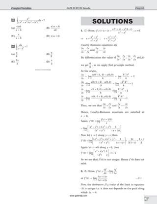
![Let Dz ® 0 along a path parallel to real axis
Þ =Dy 0 Dz ® 0 Þ Dx ® 0
Now equation (1)
¢ =
+
= +
® ® ®
f z
u i v
x
u
x
i
v
xx x x
( ) lim lim lim
D D D
D D
D
D
D
D
D0 0 0
¢ =
+
f z
u
x
i
v
x
( ) ....(2)
Again, let Dz ® 0 along a path parallel to imaginary
axis, then Dx ® 0 and Dz ® 0 ® Dy ® 0
Thus from equation (1)
¢f =
+
®
( ) limz
z i v
i yyD
D D
D0
= +
® ®
lim lim
D D
D
D
D
Dy y
u
i y
i
v
i z0 0
=
+
u
i y
v
y
¢ =
- 
+
f z
i u
y
v
y
( ) ....(3)
Now, for existence of ¢f z( ) R.H.S. of equation (2) and (3)
must be same i.e.,
+
=
-
u
x
i
v
x
v
y
i
u
y
=
u
x
v
y
and
=
-
v
x
u
y
¢ =
-
=
+
f z
u
x
i
u
y
v
y
i
v
x
( )
3. (A) Given f z x iy( ) = +2 2
since, f z u iv( ) = +
Here u x= 2
and v y= 2
Now, u x= 2
Þ
=
u
x
x2 and
=
u
y
0
and v y= 2
Þ
=
v
x
0 and
=
v
y
y2
we know that ¢ =
-
f z
u
x
i
u
y
( ) ....(1)
and ¢ =
+
f z
v
y
i
v
x
( ) ....(2)
Now, equation (1) gives ¢ =f z x( ) 2 ....(3)
and equation (2) gives ¢ =f z y( ) 2 ....(4)
Now, for existence of ¢f z( ) at any point is necessary that
the value of ¢f z( ) most be unique at that point, whatever
be the path of reaching at that point
From equation (3) and (4) 2 2x y=
Hence, ¢f z( ) exists for all points lie on the line x y= .
4. (B)
= -
u
x
y2 1( ) ;
=
2
2
0
u
x
....(1)
= -
u
y
x2 ;
=
2
2
0
u
y
....(2)
Þ
+
=
2
2
2
2
0
u
x
u
y
, Thus u is harmonic.
Now let v be the conjugate of u then
dv
v
x
dx
v
y
dy=
+
= -
+
u
y
dx
u
x
dy
(by Cauchy-Riemann equation)
Þ = + -dv x dx y dy2 2 1( )
On integrating v x y y C= - + +2 2
2
5. (C) Given f z u i v( ) = + ....(1)
Þ = - +if z v iu( ) ....(2)
add equation (1) and (2)
Þ + = - + +( ) ( ) ( ) ( )1 i f z u v i u v
Þ = +F z U iV( )
where, F z i f z( ) ( ) ( )= +1 ; U u v= -( ); V u v= +
Let F z( ) be an analytic function.
Now, U u v e y yx
= - = -(cos sin )
= -
U
x
e y yx
(cos sin ) and
= - -
U
y
e y yx
( sin cos )
Now, dV
U
y
dx
U
x
dy=
-
+
....(3)
= + + -e y y dx e y y dyx x
(sin cos ) (cos sin )
= +d e y yx
[ (sin cos )]
on integrating V e y y cx
= + +(sin cos ) 1
F z U iV e y y ie y y icx x
( ) (cos sin ) (sin cos )= + = - + + + 1
= + + + +e y i y ie y i y icx x
(cos sin ) (cos sin ) 1
F z i e ic i e icx iy z
( ) ( ) ( )= + + = + ++
1 11 1
( ) ( ) ( )1 1 1+ = + +i f z i e icz
Þ = +
+
= +
-
+ -
f z e
i
i
c e c
i i
i i
z z
( )
( )
( )( )1
1
1 1
1 1 = +
+
e
i
cz ( )1
2
1
Þ = + +f z e i cz
( ) ( )1
6. (C) u x y= sinh cos
= = f
u
x
x y x ycosh cos ( , )
and
= - = y
u
y
x y x ysinh sin ( , )
by Milne’s Method
¢ = f - y = - × =f z z i z z i z( ) ( , ) ( , ) cosh cosh0 0 0
On integrating f z z( ) sinh= + constant
Þ = = +f z w z ic( ) sinh
(As u does not contain any constant, the constant c is in
the function x and hence i.e. in w).
7. (A)
= =
v
x
y h x y2 ( , ),
= =
v
y
x g x y2 ( , )
by Milne’s Method ¢ = +f z g z ih z( ) ( , ) ( , )0 0 = + =2 0 2z i z
On integrating f z z c( ) = +2
Page
568
Engineering MathematicsUNIT 9 GATE EC BY RK Kanodia
www.gatehelp.com](https://image.slidesharecdn.com/a-150815031147-lva1-app6892/85/A-gate-by-rk-kanodia-372-320.jpg)
![8. (D)
=
- + - -
+
v
y
x y x y y
x y
( ) ( )
( )
2 2
2 2 2
2
=
- -
+
=
y x xy
x y
g x y
2 2
2 2 2
2
( )
( , )
=
+ - -
+
=
- +
+
=
v
x
x y x y x
x y
y x xy
x y
h x
( ) ( )
( ) ( )
(
2 2
2 2 2
2 2
2 2 2
2 2
, )y
By Milne’s Method
¢ = +f z g z ih z( ) ( , ) ( , )0 0 = - + -
æ
è
ç
ö
ø
÷ = - +
1 1
1
1
2 2 2
z
i
z
i
z
( )
On integrating
f z i
z
dz c i
z
c( ) ( ) ( )= + + = + +ò1
1
1
1
2
9. (A)
=
- -
-
u
x
x y x x
y x
2 2 2 2 2 2
2 2
2
2
cos (cosh cos ) sin
(cosh cos )
=
-
-
= f
2 2 2 2
2 2 2
cos cosh
(cosh cos )
( , )
x y
y y
x y
=
-
= y
u
y
x y
y x
x y
2 2 2
2 2 2
sin sinh
(cosh cos )
( , )
By Milne’s Method
¢ = f - yf z z i z( ) ( , ) ( , )0 0
=
-
-
- =
-
-
= -
2 2 2
1 2
0
2
1 22
2cos
( cos )
( )
cos
z
z
i
z
zcosec
On integrating
f z z dz ic z ic( ) cot= - + = +òcosec2
10. x at b= + , y ct d= +
On A, z i= +1 and On B, z i= +2 4
Let z i= +1 corresponds to t = 0
and z i= +2 4 corresponding to t = 1
then, t = 0 Þ x b= , y d=
Þ b = 1, d = 1
and t = 1 Þ x a b= + , y c d= +
Þ 2 1= +a , 4 1= +c Þ a = 1, c = 3
AB is , y t= +3 1 Þ dx dt= ; dy dt= 3
f z dz x ixy dx idy
c c
( ) ( )( )ò ò= + +2
= + + + + +
=
ò[( ) ( )( )][ ]t i t t dt i dt
t
1 1 3 1 32
0
1
= + + + + + +ò[( ) ( )]( )t t i t t i dt2 2
0
1
2 1 3 4 1 1 3
= + + + + + +
é
ë
ê
ù
û
ú( ) ( )1 3
3
2
3
2 3 2
0
1
i
t
t t i t t t = - +
29
3
1 1i
11. (D) We know by the derivative of an analytic
function that
¢¢ =
- +òf z
n
i
f z dz
z z
o
o
n
c
( )
! ( )
( )2 1
p
or
f z dz
z z
i
n
f z
o
n
c
n
o
( )
( ) !
( )
-
=+ò 1
2p
Taking n = 3,
f z dz
z z
i
f z
oc
o
( )
( )
( )
-
= ¢¢ò 4
3
p
....(1)
Given f
e dz
z
e dz
z
c
z z
c
2
4
2
4
1 1( ) [ ( )]+
=
- -ò
Taking f z e z
( ) = 2
, and zo = -1 in (1), we have
e dz
z
i
f
z
c
2
4
1 3
1
( )
( )
+
= ¢¢¢ -ò
p
....(2)
Now, f z e z
( ) = 2
Þ ¢¢¢ =f z e z
( ) 8 2
Þ ¢¢¢ - = -
f e( )1 8 2
equation (2) have
Þ
+
=ò
-e dz
z
i
e
z
c
2
4
2
1
8
3( )
p
....(3)
If is the circle z = 3
Since, f z( ) is analytic within and on z = 3
e dz
z
i
e
z
z
z
2
4
3
1
8
3( )| | +
=
=
-
ò
p
12. (D) Since,
1 2
1 2
1
2
1
1
3
2 2
-
- -
= +
-
-
-
z
z z z z z z( )( ) ( )
1 2
1 2
-
- -ò
z
z z z
dz
c ( )( )
= + -
1
2
3
2
1 2 3I I I ....(1)
Since, z = 0 is the only singularity for I
z
dz
c
1
1
= ò and it
lies inside z = 15. , therefore by Cauchy’s integral
Formula
I
z
dz i
c
1
1
2= =ò p ....(2)
f z
i
f z dz
z z
o
oc
( )
( )
=
-
é
ë
ê
ù
û
úò
1
2p
[Here f z f zo( ) ( )= =1 and zo = 0]
Similarly, for I
z
dz
c
2
1
1
=
-ò , the singular point z = 1 lies
inside z = 15. , therefore I i2 2= p ....(3)
For I
z
dz
c
3
1
2
=
-ò , the singular point z = 2 lies outside
the circle z = 15. , so the function f z( ) is analytic
everywhere in c i.e. z = 15. , hence by Cauchy’s integral
theorem
I
z
dz
c
3
1
2
0=
-
=ò ....(4)
using equations (2), (3), (4) in (1), we get
1 2
1 2
1
2
2 2
3
2
0
-
- -
= + -ò
z
z z z
dz i i
c ( )( )
( ) ( )p p = 3pi
13. (B) Given contour c is the circle z = 1
Chap 9.5
Page
569
Complex Variables GATE EC BY RK Kanodia
www.gatehelp.com](https://image.slidesharecdn.com/a-150815031147-lva1-app6892/85/A-gate-by-rk-kanodia-373-320.jpg)
![Þ =z eiq
Þ dz ie di
= q
q
Now, for upper half of the circle, 0 £ £q p
( ) ( )z z dz e e ie d
c
i i i
- = -ò ò=
2
0
2q
q
p
q q
q
= -òi e e di i
( )2 3
0
q q
p
q = -
é
ë
ê
ù
û
úi
e
i
e
i
i i2 3
0
2 3
q q
p
= × × - - -
é
ëê
ù
ûúi
i
e ei x1 1
2
1
1
3
12 3
( ) ( )p p
=
2
3
14. (B) Let f z z( ) cos= p then f z( ) is analytic within and
on z = 3, now by Cauchy’s integral formula
f z
i
f z
z z
dzo
oc
( )
( )
=
-ò
1
2p
Þ
-
=ò
f z dz
z z
if z
oc
o
( )
( )2p
take f z z( ) cos= p , zo = 1, we have
cos
( )
p
p
z
z
dz if
z -
=
=
ò 1
2 1
3
= 2p picos = -2pi
15. (D)
sin
( )( )
pz
z z
dz
c
2
1 2- -ò
=
-
-
-ò ò
sin sinp pz
z
dz
z
z
dz
c c
2 2
2 1
= -2 2 2 1p pif if( ) ( ) since, f z z( ) sin= p 2
Þ = =f( ) sin2 4 0p and f( ) sin1 0= =p
16. (D) Let, I
i z
z dz
c
=
-ò
1
2
1
12
p
pcos
=
× -
-
+
æ
è
ç
ö
ø
÷ò
1
2 2
1
1
1
1p
p
i z z
z dz
c
cos
Or I
i
nz
z
nz
z
dz
c
=
-
-
+
æ
è
ç
ö
ø
÷ò
1
4 1 1p
cos cos
17. (D) f
z z
z
dz
c
( )3
3 7 1
3
2
=
+ +
-ò , since zo = 3 is the only
singular point of
3 7 1
3
2
z z
z
+ +
-
and it lies outside the
circle x y2 2
4+ = i.e., z = 2, therefore
3 7 1
3
2
z z
z
+ +
-
is
analytic everywhere within c.
Hence by Cauchy’s theorem—
f
z z
z
dz
c
( )3
3 7 1
3
0
2
=
+ +
-
=ò
18. (C) The point ( )1 - i lies within circle z = 2 ( ... the
distance of 1 - i i.e., (1, 1) from the origin is 2 which is
less than 2, the radius of the circle).
Let f = + +( )z z z3 7 12
then by Cauchy’s integral formula
3 7 1
2
2
z z
z z
dz i z
oc
o
+ +
-
= fò p ( )
Þ = ff z i zo o( ) ( )2p Þ ¢ = ¢ff z i zo o( ) ( )2p
and ¢¢ = ¢¢ff z i zo o( ) ( )2p
since, f = + +( )z z z3 7 12
Þ f¢ = +( )z z6 7 and ¢¢f =( )z 6
¢ - = - +f i i i( ) [ ( ) ]1 2 6 1 7p = +2 5 13p ( )i
19. (C) f z
z
z z
( ) =
-
+
= -
+
1
1
1
2
1
Þ = -f( )0 1, f( )1 0=
Þ ¢ =
+
f z
z
( )
( )
2
1 2
Þ ¢ =f ( )0 2;
¢¢ =
-
-
f z
z
( )
( )
4
1 3
Þ ¢¢ = -f ( )0 4;
¢¢¢ =
+
f z
z
( )
( )
12
1 4
Þ ¢¢¢ =f ( )0 12; and so on.
Now, Taylor series is given by
f z f z z z f z
z z
f z( ) ( ) ( ) ( )
( )
!
( )= + - ¢ +
-
¢¢ +0 0 0
0
2
0
2
( )
!
( ) .....
z z
f z
-
¢¢¢ +0
3
0
3
about z = 0
f z z
z z
( ) ( )
!
( )
!
( ) ....= - + + - + +1 2
2
4
3
12
2 3
= - + - +1 2 2 22 3
z z z ....
f z z z z( ) ( ....)= - + - +1 2 2 3
20. (B) f z
z
( ) =
+
1
1
Þ f( )1
1
2
=
¢ =
-
+
f z
z
( )
( )
1
1 2
Þ ¢ =
-
f ( )1
1
4
¢¢ =
+
f z
z
( )
( )
2
1 3
Þ ¢¢ =f ( )1
1
4
¢¢¢ =
-
+
f z
z
( )
( )
6
1 4
Þ ¢¢¢ = -f ( )1
3
8
and so on.
Taylor series is
f z f z z z f z
z z
f z( ) ( ) ( ) ( )
( )
!
( )= + - ¢ +
-
¢¢0 0 0
0
2
0
2
+
-
¢¢¢ +
( )
!
( )
z z
f z0
3
0
3
K
about z = 1
f z z
z z
( ) ( )
( )
!
( )
!
= + -
-æ
è
ç
ö
ø
÷ +
- æ
è
ç
ö
ø
÷ +
-
-
1
2
1
1
4
1
2
1
4
1
3
32 3
8
æ
è
ç
ö
ø
÷+K
= - - + - - - +
1
2
1
2
1
1
2
1
1
2
12 3
2
4
3
( ) ( ) ( ) ....z z z
or f z z z z( ) ( ) ( ) ( ) ....= - - + - - - +
é
ëê
ù
ûú
1
2
1
1
2
1
1
2
1
1
2
12
2
3
3
Page
570
Engineering MathematicsUNIT 9 GATE EC BY RK Kanodia
www.gatehelp.com](https://image.slidesharecdn.com/a-150815031147-lva1-app6892/85/A-gate-by-rk-kanodia-374-320.jpg)
![21. (A) f z z( ) sin= Þ f
p p
4 4
1
2
æ
è
ç
ö
ø
÷ = =sin
¢ =f z z( ) cos Þ ¢æ
è
ç
ö
ø
÷ =f
p
4
1
2
¢¢ = -f z z( ) sin Þ ¢¢æ
è
ç
ö
ø
÷ = -f
p
4
1
2
¢¢¢ = -f z z( ) cos Þ ¢¢¢æ
è
ç
ö
ø
÷ = -f
p
4
1
2
and so on.
Taylor series is given by
f z f z z z f z
z z
f z( ) ( ) ( ) ( )
( )
!
( )= + - ¢ +
-
¢¢0 0 0
0
2
0
2
+
-
¢¢¢ +
( )
!
( ) ....
z z
f z0
3
0
3
about z =
p
4
f z z
z
( )
!
= + -
æ
è
ç
ö
ø
÷ +
-
æ
è
ç
ö
ø
÷
-
æ
è
ç
ç
ö
ø
÷
÷
1
2 4
1
2
4
2
1
2
2
p
p
+
-
æ
è
ç
ö
ø
÷
-
æ
è
ç
ç
ö
ø
÷
÷ +
z
p
4
3
1
2
3
!
K
f z z z z( )
! !
= + -
æ
è
ç
ö
ø
÷ - -
æ
è
ç
ö
ø
÷ - -
æ
è
ç
ö
ø
÷ -
1
2
1
4
1
2 4
1
3 4
2 3
p p p
...
é
ë
ê
ê
ù
û
ú
ú
22. (D) Let f z z( ) = -2
= =
- +
1 1
1 12 2
z z[ ( )]
f z z( ) [ ( )]= - + -
1 1 2
Since, 1 1+ <z , so by expanding R.H.S. by binomial
theorem, we get
f z z z z( ) ( ) ( ) ( )= + + + + + + +1 2 1 3 1 4 12 3
K
+ + + +( )( )n z n
1 1 K
or f z z n z n
n
( ) ( )( )= = + + +-
=
¥
å2
1
1 1 1
23. (B) Here f z
z z z z
( )
( )( )
=
- -
=
-
-
-
1
1 2
1
2
1
1
....(1)
Since, z > 1 Þ
1
1
z
< and z < 2 Þ <
z
2
1
1
1
1
1
1
1
1
1
1
z
z
z
z z-
=
-
æ
è
ç
ö
ø
÷
= -
æ
è
ç
ö
ø
÷
-
= + + + +
æ
è
ç
ö
ø
÷
1
1
1 1 1
2 3
z z z z
K
and
1
2
1
2
1
2
1
z
z
-
=
-
-
æ
è
ç
ö
ø
÷
-
= - + + + +
é
ë
ê
ù
û
ú
1
2
1
2 4 9
2 3
z z z
K
equation (1) gives—
f z
z z z
( ) ..= - + + + +
æ
è
çç
ö
ø
÷÷
1
2
1
2 4 9
2 3
- + + + +
æ
è
ç
ö
ø
÷
1
1
1 1 1
2 3
z z z z
K
or f z z z z z z z( ) = - - - - - - - -- - -
K K4 2 1 2 31
2
1
4
1
8
1
18
24. (C)
2
1
z
< Þ
1 1
2
1
z
< < Þ
1
1
z
<
1
1
1
1
1 1
2
1
1 1 1
1
2 3
z z z z z z-
= -
æ
è
ç
ö
ø
÷ = + + + +
æ
è
ç
ö
ø
÷
-
K
and
1
2
1
1
2 1
1
2 4 8
1
2 3
z z z z z z z-
= -
æ
è
ç
ö
ø
÷ = + + + +
æ
è
ç
ö
ø
÷
-
....
Laurent’s series is given by
f z
z z z z z z z z
( ) .. ..= + + + +
æ
è
ç
ö
ø
÷ - + + + +
æ
è
ç
1
1
2 4 98 1
1
1 1 1
2 3 2 3
ö
ø
÷
= + + +
æ
è
ç
ö
ø
÷
1 1 3 7
2 3
z z z z
K
Þ = + + +f z
z z z
( )
1 3 7
2 3 4
K
25. (B) z < 1,
1
2
1
1
1
2
1
2
1
1
1
z z
z
z
-
-
-
= - -
æ
è
ç
ö
ø
÷ + -
-
-
( )
= - + + + +
é
ë
ê
ù
û
ú + + + + +
1
2
1
2 4 8
1
2 3
2 3z z z
z z zK ( ...)
f z z z z( ) = + + + +
1
2
3
4
7
8
15
16
2 3
K
26. (D) Since,
1
1 2
1
2
1
1
1
2 2z z z z z z( )( ) ( )- -
= -
-
+
-
For z - <1 1 Let z u- =1
Þ = +z u 1 and u < 1
1
1 2
1
2
1
1
1
2 2z z z z z z( )( ) ( )- -
= -
-
+
-
=
+
- +
-
1
2 1
1 1
2 1( ) ( )u u u
= + - - -- - -1
2
1
1
2
11 1 1
( ) ( )u u u
= - + - + - - + + + +-1
2
1
1
2
12 3 1 2 3
[ ...] ( ...)u u u u u u u
= - - - - = - - - - -- -1
2
2 2 3 1 3 5 1
( ...)u u u u u u uK
Required Laurent’s series is
f z z z z z( ) ( ) ( ) ( ) ( )= - - - - - - - - --
1 1 1 11 3 5
K
27. (B) Let f z
z ez
( )
( )
=
-
1
1
=
+ + + + + -
é
ë
ê
ù
û
ú
1
1
2 3 4
1
2 3 4
z z
z z z
! ! !
K
Chap 9.5
Page
571
Complex Variables GATE EC BY RK Kanodia
www.gatehelp.com](https://image.slidesharecdn.com/a-150815031147-lva1-app6892/85/A-gate-by-rk-kanodia-375-320.jpg)
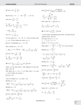
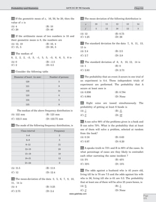
![24. The probability that a man who is x years old will
die in a year is p. Then amongst n persons
A A An1 2, , ,K each x years old now, the probability
that A1 will die in one year is
(A)
1
2
n
(B) 1 1- -( )p n
(C)
1
1 12
n
p n
[ ( ) ]- - (D)
1
1 1
n
p n
[ ( ) ]- -
25. A bag contains 4 white and 2 black balls. Another
bag contains 3 white and 5 black balls. If one ball is
drawn from each bag, the probability that both are
white is
(A)
1
24
(B)
1
4
(C)
5
24
(D) None
26. A bag contains 5 white and 4 red balls. Another bag
contains 4 white and 2 red balls. If one ball is drawn
from each bag, the probability that one is white and one
is red, is
(A)
13
27
(B)
5
27
(C)
8
27
(D) None
27. An anti-aircraft gun can take a maximum of 4 shots
at an enemy plane moving away from it. The
probabilities of hitting the plane at the first, second,
third and fourth shot are 0.4, 0.3, 0.2 and 0.1
respectively. The probability that the gun hits the plane
is
(A) 0.76 (B) 0.4096
(C) 0.6976 (D) None of these
28. If the probabilities that A and B will die within a
year are p and q respectively, then the probability that
only one of them will be alive at the end of the year is
(A) pq (B) p q( )1 -
(C) q p( )1 - (D) p pq+ -1 2
29. In a binomial distribution, the mean is 4 and
variance is 3. Then, its mode is
(A) 5 (B) 6
(C) 4 (D) None
30. If 3 is the mean and (3/2) is the standard deviation
of a binomial distribution, then the distribution is
(A)
3
4
1
4
12
+
æ
è
ç
ö
ø
÷ (B)
1
2
3
2
12
+
æ
è
ç
ö
ø
÷
(C)
4
5
1
5
60
+
æ
è
ç
ö
ø
÷ (D)
1
5
4
5
5
+
æ
è
ç
ö
ø
÷
31. The sum and product of the mean and variance of a
binomial distribution are 24 and 18 respectively. Then,
the distribution is
(A)
1
7
1
8
12
+
æ
è
ç
ö
ø
÷ (B)
1
4
3
4
16
+
æ
è
ç
ö
ø
÷
(C)
1
6
5
6
24
+
æ
è
ç
ö
ø
÷ (D)
1
2
1
2
32
+
æ
è
ç
ö
ø
÷
32. A die is thrown 100 times. Getting an even number
is considered a success. The variance of the number of
successes is
(A) 50 (B) 25
(C) 10 (D) None
33. A die is thrown thrice. Getting 1 or 6 is taken as a
success. The mean of the number of successes is
(A)
3
2
(B)
2
3
(C) 1 (D) None
34. If the sum of mean and variance of a binomial
distribution is 4.8 for five trials, the distribution is
(A)
1
5
4
5
5
+
æ
è
ç
ö
ø
÷ (B)
1
3
2
3
5
+
æ
è
ç
ö
ø
÷
(C)
2
5
3
5
5
+
æ
è
ç
ö
ø
÷ (D) None of these
35. A variable has Poission distribution with mean m.
The probability that the variable takes any of the
values 0 or 2 is
(A) e m
mm-
+ +
æ
è
çç
ö
ø
÷÷1
2
2
!
(B) e mm
( )1 3 2
+ -
(C) e m3 2 2 1 2
1( )+ -
(D) e
mm-
+
æ
è
çç
ö
ø
÷÷1
2
2
!
36. If X is a Poission variate such that
P P P( ) ( ) ( )2 9 4 90 6= + , then the mean of X is
(A) ± 1 (B) ± 2
(C) ± 3 (D) None
Page
576
Engineering MathematicsUNIT 9 GATE EC BY RK Kanodia
www.gatehelp.com](https://image.slidesharecdn.com/a-150815031147-lva1-app6892/85/A-gate-by-rk-kanodia-379-320.jpg)
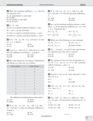
![SOLUTION
1. (B) Let the lower limit be x. Then, upper limit is
x + 4.
x x+ +
=
( )4
2
15 Þ x = 13.
2. (A) Let the lower limit be x. Then, upper limit x + 10.
x x+ +
=
( )10
2
42 Þ x = 37.
Lower limit = 37 and upper limit =47.
3. (D) Range = Difference between the largest value
= - =( )95 62 33.
4. (B) Upper class boundary = + ´ =10 6 2 5 9 331. ( . ) . .
5. (B)
Marks Frequency f f ´ 1
0 2 0
2 2 4
3 3 9
4 1 4
5 4 20
6 2 12
7 1 7
8 1 8
å =f 16 å ´ =( )f x 64
A.M. =
å ´
å
= =
( )f x
f
64
16
4.
6. (B) Mean =
´ + ´ + ´
= =
45 2 40 2 5 15 2
100
220
100
2 2
.
. .
7. (B)
Class
Mid
value x
Frequenc
y f
Deviation
d x A= -
f d´
0–10 5 12 -20 -240
10–20 15 18 -10 -180
20–30 25 = A 27 0 0
30–40 35 20 10 200
40–50 45 17 20 320
50–60 55 6 30 180
Sf = 100 S ( )f d´ = 390
A.M. = + = +
æ
è
ç
ö
ø
÷ =A
fd
f
S
S
( )
25
300
100
28.
8. (C) Since 8 occurs most often, mode =8.
9. (B) Clearly, 46 occurs most often. So, mode =46.
10. (B) ( )x ´ ´ =16 50 201 3
Þ x ´ ´ =16 50 20 3
( )
Þ x =
´ ´
´
æ
è
çç
ö
ø
÷÷ =
20 20 20
16 50
10.
11. (B) Let the numbers be a and b Then,
a b
a b
+
= Þ + =
2
10 20( ) and
ab ab= Þ =8 64
a b a b ab- = + - = - = =( )2
4 44 256 144 12.
Solving a b+ = 20 and a b- = 12 we get a = 16 and
b = 4.
12. (D) Observations in ascending order are
-3, -3, -1, 0, 2, 2, 2, 5, 5, 5, 5 6, 6, 6
Number of observations is 14, which is even.
Median =
1
2
7[ the term +8 the term] = + =
1
2
2 5 35( ) . .
13. (A) The given Table may be presented as
Diameter of heart
(in mm)
Number of
persons
Cumulative
frequency
120 5 5
121 9 14
122 14 28
123 8 36
124 5 41
125 9 50
Here n = 50. So,
n
2
25= and
n
2
1 26+ = .
Medium =
1
2
(25th term +26 th term) =
+
=
122 122
2
122.
[ ... Both lie in that column whose c.f. is 28]
14. (B) Maximum frequency is 23. So, modal class is
12–15.
L1 12= , L2 15= , f = 23, f1 21= and f2 10= .
Thus Mode = +
-
- -
-L
f f
f f f
L L1
1
1 2
2 1
2
( )
Page
578
Engineering MathematicsUNIT 9 GATE EC BY RK Kanodia
www.gatehelp.com](https://image.slidesharecdn.com/a-150815031147-lva1-app6892/85/A-gate-by-rk-kanodia-381-320.jpg)
![= +
-
- -
- =12
23 21
46 21 10
15 12 12 4
( )
( )
( ) . .
15. (C) Mean =
+ + + + + + +æ
è
ç
ö
ø
÷ =
3 5 6 7 8 10 11 14
8
8.
Sd = - + - + - + - + - + -3 8 5 8 8 8 10 8 11 8 14 8
= 22
Thus Mean deviation = = =
Sd
n
22
8
2 75. .
16. (B)
x f f x´ d = -x M f ´ d
10 3 30 2 6
11 12 132 1 12
12 18 216 0 0
13 12 156 1 12
14 3 42 2 6
Sf = 48 Sfx = 576 Sfd = 36
Thus M = =
576
48
12.
So, Mean deviation = = =
Sf
n
d 36
48
0 75.
17. (D) m =
+ + + +
= =
7 9 11 13 15
5
55
5
11.
Sd2 2 2 2 2 2
7 11 9 11 11 11 13 11 15 11 40= - + - + - + - + - =
s
d
= =
S 2
40
5n
= = = ´ =8 2 2 2 141 28. . .
18. (C) M =
+ + + +
= =
6 8 10 12 14
5
50
5
10.
Sd2 2 2 2 2 2
6 10 8 10 10 10 12 10 14 10 40= - + - + - + - + - =
6
40
5
2
= =
Sd
n
= = = ´ =8 2 2 2 1 414 2 83. . (app.)
19. (B) Here p = 0.4, q = 0.6 and n = 3.
Required probability = P(A occurring at least once)
= × ´ + × ´3
1
2 3
2
2
0 4 0 6 0 4 0 6C C( . ) ( . ) ( . ) ( . ) + ×3
3
3
0 4C ( . )
= ´ ´ + ´ ´ +
æ
è
ç
ö
ø
÷3
4
10
36
100
3
16
100
6
10
64
1000
= =
784
1000
0 784. .
20. (B) p =
1
2
, q =
1
2
, n = 8. Required probability
= P (6 heads or 7 heads or 8 heads)
= ×
æ
è
ç
ö
ø
÷ ×
æ
è
ç
ö
ø
÷ + ×
æ
è
ç
ö
ø
÷ × + ×
æ
è
8
6
6 2
8
7
7
8
8
1
2
1
2
1
2
1
2
1
2
C C C ç
ö
ø
÷
8
=
´
´
´ + ´ + =
8 7
2 1
1
256
8
1
256
1
256
37
256
21. (C) Let E = the event that A solves the problem. and
F = the event that B solves the problem.
Clearly E and F are independent events.
P E P F( ) . , ( ) .= = = =
90
100
0 9
70
100
0 7,
P E F P E P F( ) ( ) ( ) . . .º = × = ´ =0 9 0 7 0 63
Required probability = ÈP E F( )
= + - ºP E P F P E F( ) ( ) ( ) = (0.9 +0.7 - 0.63) =0.97.
22. (C) Let E =event that A speaks the truth.
F =event that B speaks the truth.
Then, P E( ) = =
75
100
3
4
, P F( ) = =
80
100
4
5
P E( ) = -
æ
è
ç
ö
ø
÷ =1
3
4
1
4
, P F( ) = -
æ
è
ç
ö
ø
÷ =1
4
5
1
5
P (A and B contradict each other).
= P[(A speaks truth and B tells a lie) or (A tells a lie and
B speaks the truth)]
= P (E and F ) + P (E and F)
= × + ×P E P F P E P F( ) ( ) ( ) ( )
= ´ + ´ = + =
3
4
1
5
1
4
4
5
3
20
1
5
7
20
= ´
æ
è
ç
ö
ø
÷ =
7
20
100 35% %.
23. (A) Let E = event that the husband will be alive 25
years hence and F =event that the wife will be alive 25
years hence.
Then, P E( ) =
5
12
and P F( ) =
3
8
Thus P E( ) = -
æ
è
ç
ö
ø
÷ =1
5
12
7
12
and P F( ) = -
æ
è
ç
ö
ø
÷ =1
3
8
5
8
.
Clearly, E and F are independent events.
So, E and F are independent events.
P(at least one of them will be alive 25 years hence)
= -1 P(none will be alive 24 years hence)
= - º1 P E F( ) = - × = - ´
æ
è
ç
ö
ø
÷ =1 1
7
12
5
8
61
96
P E P F( ) ( )
24. (D) P(none dies)
= - -( ) ( )1 1p p ....n times = -( )1 p n
P(at least one dies) = - -1 1( )p n
.
P(A1 dies) =
1
n
{1 1- -( )p n
}.
Chap 9.6
Page
579
Probability and Statistics GATE EC BY RK Kanodia
www.gatehelp.com](https://image.slidesharecdn.com/a-150815031147-lva1-app6892/85/A-gate-by-rk-kanodia-382-320.jpg)
![39. (C) x
x
n
i
= = =
S 15
5
3, y
y
n
i
=
å
= =
36
5
7 2.
cov( , )x y
x y
n
x yi i
= -
æ
è
ç
ö
ø
÷
S
= - ´
æ
è
ç
ö
ø
÷ =
110
5
3 7 2 0 4. .
40. (D) r
x y
x var y
=
×
=
-
´
= -
cov
var
( , )
( ) ( )
.
.
.
16 5
2 89 100
0 97.
41. (B) Di = - - - -2 8 2 3 3 3, , , , , , 3, 0, 2, 4.
SDi
2
4 64 4 9 9 9 9 0 4 16 128= + + + + + + + + + =( ) .
R
D
n n
i
= -
-
é
ë
ê
ù
û
ú = -
´
´
æ
è
çç
ö
ø
÷÷ =1
6
1
1
6 128
10 99
37
16
2
2
( )
( )
S
5
0 224= . .
42. (A) b
x y
x y
n
x
x
n
yx
i i
i i
i
i
=
-
-
é
ë
ê
ù
û
ú
S
S S
S
S
( )( )
( )2
2
=
-
´æ
è
ç
ö
ø
÷
-
é
ë
ê
ù
û
ú
=
-
-
306
24 44
4
164
24
4
306 264
164 142
( )
( )
( 4
42
20
2 1
)
.= =
43. (B) b
x y
x y
n
y
y
n
yx
i i
i i
i
i
=
-
é
ëê
ù
ûú
-
é
ë
ê
ù
û
ú
=
-S
S S
S
S
( )( )
( )2
2
199
30 42
6
318
42 42
6
´æ
è
ç
ö
ø
÷
-
´é
ëê
ù
ûú
=
-
-
=
-
= -
( )
( )
.
199 210
318 294
11
24
0 46.
44. (C) b r
y
x
yx = ×
s
s
and b r
x
y
xy = ×
s
s
r b bxy yx
2
= ´ Þ r b bxy yx= ´ .
45. (C)
1
2
( )b b rxy yx+ > is true if
1
2
r
y
x
r
x
y
r× + ×
é
ë
ê
ù
û
ú >
s
s
s
s
i.e. if s s s sy x x y
2 2
2+ >
i.e. if ( )s sy x- >2
0, which is true.
46. (A) r = ´ = =1 6 0 4 64 0 8. . . .
b ryx
y
x
= ×
s
s
Þ
s
s
y
x
yxb
r
= = =
1 6
0 8
2
.
.
m
r
y
x
1
1 1
0 8
2
5
2
= × = ´ =
s
s .
, m r
y
x
2 0 8 2 1 6= × = ´ =
s
s
. . .
tan
. .
. .
q =
-
+
æ
è
çç
ö
ø
÷÷ =
-
+ ´
æ
è
çç
ö
ø
÷÷ =
m m
m m
1 2
1 21
2 5 1 6
1 2 5 1 6
0 9
5
0 18
.
.= .
47. (C) Given lines are : y x= - -2
3
4
and x y= - -
æ
è
ç
ö
ø
÷
7
4
3
4
byx =
-3
4
and bxy =
-3
4
.
So, r2 3
4
3
4
9
16
=
-
´
-æ
è
ç
ö
ø
÷ = or r = - = -
3
4
0 75. .
[... byx and bxy are both negative ® r is negative]
48. (A) r( , )
cov( , )
var( ) var( )
X Y
X Y
X Y
= =
´
=
10
6 25 31 36
5
7. .
49. (C) b
n xy x y
n x x
yx =
-
-
S S S
S S
( )( )
( )2 2
=
´ - ´
´ - ´
æ
è
çç
ö
ø
÷÷ = -
5 44 15 15
5 49 15 15
1
4
50. (B) b
n xy x y
n y y
xy =
-
-
S S S
S S
( )( )
( )2 2
=
´ - ´
´ - ´
=
25 50 125 100
25 1500 100 100
9
22
Also, x = =
125
25
5, y = =
100
25
4.
Required line is x x b y yxy= + -( )
Þ x y= + -5
9
22
4( ) Þ 22 9 74x y- = .
Chap 9.6
Page
581
Probability and Statistics GATE EC BY RK Kanodia
www.gatehelp.com](https://image.slidesharecdn.com/a-150815031147-lva1-app6892/85/A-gate-by-rk-kanodia-383-320.jpg)
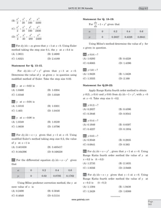

![= + -ò2 2
0
( )x dx
x
= + -2 2
2
2
x
x
....(1)
The second approximation to y is given by
y y f x y dx
x
x
( ) ( )
( , )2
0
1
0
= + ò
= + + -
æ
è
çç
ö
ø
÷÷ò2 2 2
2
2
0
f x x
x
dx
x
x
,
= + + - -ò2 2 2
2
2
0
2
( )x
x
x dx
= + + -2 2
2 6
2 3
x
x x
....(2)
The third approximation to y is given by
y y f x y dx
x
x
( ) ( )
( , )3
0
2
0
= + ò
= + + + -
æ
è
çç
ö
ø
÷÷ò2 2 2
2 6
2 3
0
f x x
x x
dx
x
x
,
= + + + - -
æ
è
çç
ö
ø
÷÷ò2 2 2
2 6
2 3
0
x
x x
dx
x
= + + + -2 2
2 6 24
2 3 4
x
x x x
11. (B) Here f x y x y x y( , ) ,= + = =2
0 00 0
We have, by Picard’s method
y y f x y dx
x
x
= + ò0 0
0
( , )
The first approximation to y is given by
y y f x y dx
x
x
( )
( , )1
0 0
0
= + ò = + ò0 0
0
f x dx
x
( , )
= + ò0
0
xdx
x
=
x2
2
The second approximation to y is given by
y y f x y dx
x
x
( ) ( )
( , )2
0
1
0
= + ò = +
æ
è
çç
ö
ø
÷÷ò0
2
2
0
f x
x
dx
x
,
= +
æ
è
çç
ö
ø
÷÷ò x
x
dx
x 4
0
4
= +
x x2 5
2 50
The third approximation is given by
y y f x y dx
x
x
( ) ( )
( , )3
0
2
0
= + ò
= + +
æ
è
çç
ö
ø
÷÷ò0
2 20
2 5
0
f x
x x
dx
x
,
= + + +
æ
è
çç
ö
ø
÷÷ò x
x x x
dx
x 4 10 7
0
4 400
2
40
= + + +
x x x x2 5 8 11
2 20 160 4400
12. (A) x: . . . .0 0 1 0 2 0 3 0 4
Euler’s method gives
y y h x yn n n n+ = +1 ( , ) ....(1)
n = 0 in (1) gives
y y hf x y1 0 0 0= + ( , )
Here x y h0 00 1 0 1= = =, , .
y f1 1 0 1 0 1= + . ( , ) = +1 0 = 1
n = 0 in (1) gives y y h f x y2 1 1 1= + ( , )
= +1 0 1 0 1 1. ( . , )f = +1 0 1 0 1. ( . ) = +1 0 01.
Thus y y2 0 2 101= =( . ) .
n = 2 in (1) gives
y y hf x y3 2 2 2= + ( , ) = +101 0 1 0 2 101. . ( . , . )f
y y3 0 3 101 0 0202 10302= = + =( . ) . . .
n = 3 in (1) gives
y y hf x y4 3 3 3= + ( , ) = +10302 0 1 0 3 10302. . ( . , . )f
= +10302 0 03090. .
y y4 0 4 10611= =( . ) .
Hence y( . ) .0 4 10611=
13. (B) The Euler’s modified method gives
y y hf x y1 0 0 0
*
= + ( , ),
y y
h
f x y f x y1 0 0 0 1 1
2
= + +[ ( , ) ( , )]*
Now, here h y x= = =0 02 1 00 0. , ,
y f1 1 0 02 0 1*
. ( , )= + , y1 1 0 02*
.= + = 102.
Next y y
h
f x y f x y1 0 0 0 1
2
= + +[ ( , ) ( , )]*
= + +1
0 02
2
0 1 0 02 102
.
[ ( , ) ( . , . )]f f
= + + =1 0 01 1 10204 10202. [ . ] .
So, y y1 0 02 10202= =( . ) .
14. (D) y y h f x y2 1 1 1
*
= + ( , )
= +10202 0 02 0 02 10202. . [ ( . , . )]f
= +10202 0 0204. . = 10406.
Next y y
h
f x y f x y2 1 2 2
2
= + +[ ( , ) ( , )]*
y f f2 10202
0 02
2
0 02 10202 0 04 10406= + +.
.
[ ( . , . ) ( . , . )]
= + + =10202 0 01 10206 10422 10408. . [ . . ] .
y y2 0 04 10408= =( . ) .
15. (C) y y hf x y3 2 2 2
*
( , )= +
= +10416 0 02 0 04 10416. . ( . , . )f
= + =10416 0 0217 10633. . .
Next y y
h
f x y f x y3 2 2 2 3 3
2
= + +[ ( , ) ( , )]*
Page
586
Engineering MathematicsUNIT 9 GATE EC BY RK Kanodia
www.gatehelp.com](https://image.slidesharecdn.com/a-150815031147-lva1-app6892/85/A-gate-by-rk-kanodia-387-320.jpg)
![k hf x h y k2 0 0 1
1
2
1
2
= + +
æ
è
ç
ö
ø
÷, = =( . ) ( . , . ) .0 2 0 1 0 1 0 202f
k hf x h y k3 0 0 2
1
2
1
2
= + +
æ
è
ç
ö
ø
÷, = ( . ) ( . , . )0 2 0 1 0 101f = 0 2020.
k hf x h y k4 0 0 3= + +( , ) = 0 2 0 2 0 2020. ( . , . )f = 0 20816.
k k k k k= + + +
1
6
2 21 2 3 4[ ]
= + + +
1
6
0 2 2 202 2 20204 0 20816[ . (. ) (. ) . ],
k = 0 2027.
such that y y y k1 00 2= = +( . ) = + =0 0 2027 0 2027. .
21. (C) We now to find y y2 0 4= ( . ), k hf x y1 1 1= ( , )
= ( . ) ( . , . )0 2 0 2 0 2027f = 0 2 10410. ( . ) = .2082
k hf x h y k2 1 1 1
1
2
1
2
= + +
æ
è
ç
ö
ø
÷,
= ( . ) ( . , . )0 2 0 3 0 3068f = 0 2188.
k hf x h y k3 1 1 2
1
2
1
2
= + +
æ
è
ç
ö
ø
÷,
= 0 2 0 3 0 3121. ( . , . )f = .2194
k hf x h y k4 1 1 3= + +( , ) = 0 2 0 4 4221. ( . , . )f = 0 2356.
k k k k k= + + +
1
6
2 21 2 3 4[ ]
= + + +
1
6
0 2082 2 2188 2 2194 0 356[ . (. ) (. ) . ] = 0 2200.
y y y k2 0 4 1= = +( . ) = + =0 2200 2027 0 4227. . .
22. (C) We now to find y y3 0 6= ( . ) , k hf x y1 2 2= ( , )
= ( . ) ( . , . )0 2 0 4 0 4228f = 0 2357.
k hf x h y k2 2 2 1
1
2
1
2
= + +
æ
è
ç
ö
ø
÷,
= ( . ) ( . , . )0 2 0 5 0 5406f = 0 2584.
k hf x h y k3 2 2 2
1
2
1
2
= + +
æ
è
ç
ö
ø
÷,
= 0 2 0 5 5520. ( . , . )f = 0 2609.
k k k k k4 1 2 3 4
1
6
2 2= + + +[ ]
= + + +
1
6
0 2357 2 2584 2 0 2609 0 2935[ . (. ) ( . ) . ]
= + + + =
1
6
0 2357 0 5168 0 5218 0 2935 0 2613[ . . . . ] .
y y y k3 0 6 2= = +( . ) = +. .4228 0 2613 = 0 6841.
23. (A) Here given x y0 00 1= = , h = 0 2.
f x y x y( , ) = + 2
To find y y1 0 2= ( . ) ,
k hf x y1 0 0= ( , ) = ( . ) ( , )0 2 0 1f = ´ =( . ) .0 2 1 0 2
k hf x
h
y
k
2 0 0
1
2 2
= + +
æ
è
ç
ö
ø
÷,
= ( . ) ( . , . )0 2 0 1 11f = 0 2 1 31. ( . ) = 0 262.
k hf x
h
y
k
3 0 0
2
2 2
= + +
æ
è
ç
ö
ø
÷,
= 0 2 0 1 1131. ( . , . )f = 0 2758.
k hf x h y k4 0 0 3= + +( , )
= =( . ) ( . , . ) .0 2 0 2 12758 0 3655f
k k k k k= + + +
1
6
2 2 21 2 3 4[ ]
= + + +
1
6
0 2 2 0 262 2 0 2758 0 3655[ . ( . ) ( . ) . ] = 0 2735.
Here y y y k1 0 2 0= = +( . ) = + Þ1 0 2735 12735. .
24. (C) Here f x y x y h( , ) .= + = 0 2
To find y y1 0 2= ( . ) ,
k hf x y1 0 0= ( , ) = 0 2 0 1. ( , )f = 0 2.
k hf x
h
y
k
2 0 0
1
2 2
= + +
æ
è
ç
ö
ø
÷, = ( . ) ( . , . )0 2 0 1 11f = 0 24.
k hf x
h
y
k
3 0 0
2
2 2
= + +
æ
è
ç
ö
ø
÷, = =( . ) ( . , . ) .0 2 0 1 112 0 244f
k hf x h y k4 0 0 3= + +( , ) = ( . ) ( . , . )0 2 0 2 1244f = 0 2888.
k k k k k= + + +
1
6
2 21 2 3 4[ ]
= + + +
1
6
0 2 2 0 24 2 0 244 0 2888[ . ( . ) ( . ) . ] = 0 2428.
y y y k1 0 2 0= = +( . ) = +1 0 2428. = 12428.
***********
Page
588
Engineering MathematicsUNIT 9 GATE EC BY RK Kanodia
www.gatehelp.com](https://image.slidesharecdn.com/a-150815031147-lva1-app6892/85/A-gate-by-rk-kanodia-388-320.jpg)
![1. If E Denotes expectation, the variance of a random
variable X is given by
(A) E X E X[ ] [ ]2 2
- (B) E X E X[ ] [ ]2 2
+
(C) E X[ ]2
(D) E X2
[ ]
2. The following plot shows a function y which varies
linearly with X. The value of the integral I y dx= ò1
2
is
(A) 1.0 (B) 2.5
(C) 4.0 (D) 5.0
3. For x << 1, coth( )x can be approximated as
(A) x (B) x2
(C)
1
x
(D)
1
2
x
4.
( )lim
sin
q
q
q®0
2/
is
(A) 0.5 (B) 1
(C) 2 (D) not defined
5. Which of the following functions is strictly bounded ?
(A)
1
2
x
(B) ex
(C) x2
(D) e x- 2
6. For the function e x-
, the linear approximation around
x = 2 is
(A) ( )3 2
- -
x e (B) 1 - x
(C) [ ( ]3 2 2 1 1 2 2
+ - + -
x e (D) e-2
7. An independent voltage source in series with an
impedance Z R jXs s s= + delivers a maximum average
power to a load impedance ZL when
(A) Z R jXL S S= + (B) Z RL S=
(C) Z jXL S= (D) Z R jXL S S= -
8. The RC circuit shown in the figure is
(A) a low-pas filter (B) a high-pass filter
(C) a band-pass filter (D) a band-reject filter
9. The electron and hole concentrations in an intrinsic
semiconductor are ni per cm3
at 300 K. Now, if acceptor
impurities are introduced with a concentration of NA
per cm3
(where N nA i>> ) the electron concentration per
cm3
at 300 K will be
(A) ni (B) n Ni A+
(C) N nA i- (D)
n
N
i
A
2
CHAPTER
10.5
Page
639
EC-07
1 2
2
3
3
-1
1
x
y
Vo
R
R C
C
-
+
Vi
-
+
GATE EC BY RK Kanodia
www.gatehelp.com](https://image.slidesharecdn.com/a-150815031147-lva1-app6892/85/A-gate-by-rk-kanodia-389-320.jpg)
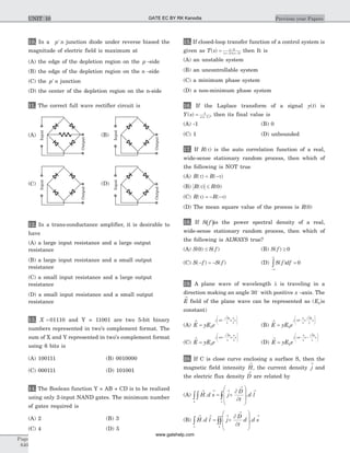

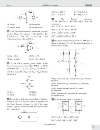
![(C) X AB BC AC= + +
(D) X A B B C AC= + +
44. The following binary values were applied to the X
and Y inputs of NAND latch shown in the figure in the
sequence indicated below
X Y X Y X Y= = = = = =0 1 0 0 1 1, ; , ; , .
The corresponding stable P Q, outputs will be
(A) P Q P Q P Q P Q= = = = = = = =1 0 1 0 1 0 0 1, ; , ; , ,or
(B) P Q P Q P Q= = = = = =1 0 0 1 0 1, ; , ; ,or P = 0Q = 1;
(C) P Q P Q P Q P Q= = = = = = = =1 0 1 1 1 0 0 1, ; , ; , ,or
(D)P Q P Q P Q= = = = = =1 0 1 1 1 1, ; , ; ,
45. For the circuit shown, the counter state ( )Q Q1 0
follows the sequence
(A) 00, 01, 10, 11, 00 (B) 00, 01, 10, 00, 01
(C) 00, 01, 11, 00, 01 (D) 00, 10, 11, 00, 10
46. An 8255 chip is interfaced to an 8085
microprocessor system as an I/O mapped I/O as show in
the figure. The address lines A0 and A1 of the 8085 are
used by the 8255 chip to decode internally its thee ports
and the Control register. The address lines A3 to A7 as
well as the IO/M signal are used for address decoding.
The range of addresses for which the 8255 chip would
get selected is
(A) F8H - FBH (B) F8H - FCH
(C) F8H - FFH (D) F0H - F7H
47. (A) The 3-dB bandwidth of the low-pas signal e u tt-
( ),
where u t( ) is the unit step function, is given by
(A)
1
2p
Hz (B)
1
2
2 1
p
- Hz
(C) ¥ (D) 1 Hz
48. A Hilbert transformer is a
(A) non-linear system (B) non-causal system
(C) time-varying system (D) low-pass system
49. The frequency response of a linear, time-invariant
system is given by H f j f
( ) = +
5
1 10p
. The step response of
the system is
(A) ( ) ( )5 1 5
- -
e u tt
(B) ( )5 1 5
-
æ
è
ç
ç
ö
ø
÷
÷
-
e u t
t
(C) ( ) ( )
1
2
1 5
- -
e u tt
(C) ( )
1
5
1 5
-
æ
è
ç
ç
ö
ø
÷
÷
-
e u t
t
50. A 5-point sequence x n[ ] is given as
x x x x x[ ] , [ ] , [ ] , [ ] , [ ]- = - = - = = =3 1 2 1 1 0 0 5 1 1. Let X ej
( )w
denote the discrete-time Fourier transform of x n[ ]. The
value of X e dj
( )w
p
p
w
-
ò is
(A) 5 (B) 10p
(C) 16p (D) 5 10+ j p
51. The z-transform x z[ ] of a sequence x n[ ] is given by
X z z
( ) .
= - -
0 5
1 2 1
. It is given that the region of convergence of
x n[ ] includes the unit circle. The value of x[0] is
(A) -0.5 (B) 0
(C) 0.25 (D) 0.5
52. A Control system with PD controller is shown in
the figure If the velocity error constant KV = 1000 and
the damping ration z = 0 5. , then the value of KP and KD
are
(A) K KP D= =100 0 09, . (B) K KP D= =100 0 9, .
(C) K KP D= =10 0 09, . (D) K KP D= =10 0 9, .
53. The transfer function of a plant is
( )
( )( )
T s
s s s
=
+ + +
5
5 12
Page
644
Previous year PapersUNIT 10
P
X
Y
Q
D1 Q1D0
Q0
8255
R s( ) C s( )
+
GATE EC BY RK Kanodia
www.gatehelp.com](https://image.slidesharecdn.com/a-150815031147-lva1-app6892/85/A-gate-by-rk-kanodia-393-320.jpg)

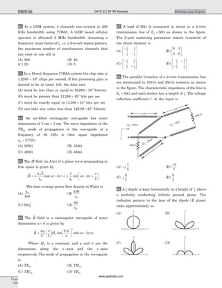

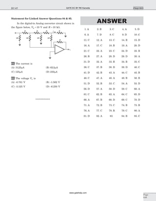

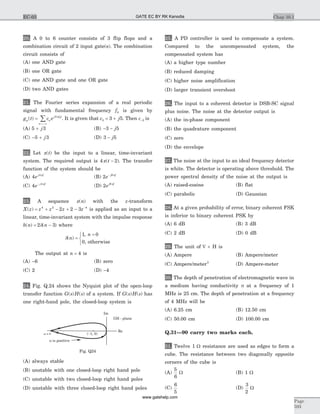
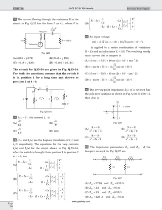

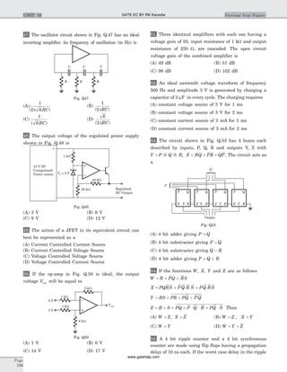
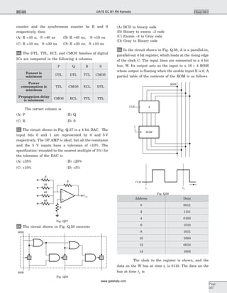
![(A) 1111 (B) 1011
(C) 1000 (D) 0010
60. In an 8085 microprocessor, the instruction CMP B
has been executed while the content of the accumulator
is less than that of register B. As a result
(A) Carry flag will be set but Zero flag will be reset
(B) Carry flag will be reset but Zero flag will be set
(C) Both Carry flag and Zero flag will be reset
(D) Both Carry flag and Zero flag will be set
61. Let X and Y be two statistically independent
random variables uniformly distributed in the ranges
( , )-1 1 and (( , )-2 1 respectively. Let Z X Y= + . Then the
probability that ( )Z £ - 2 is
(A) zero (B) 1
6
(C) 1
3
(D) 1
12
62. Let P be linearity, Q be time-invariance, R be
causality and S be stability. A discrete time system has
the input-output relationship,
y n
x n n
n
x n n
( )
( )
,
( )
=
³
=
+ £ -
ì
í
ï
î
ï
1
0 0
1 1
where x n( ) is the input and y n( ) is the output. The
above system has the properties
(A) P, S but not Q, R (B) P, Q, S but not R
(C) P, Q, R, S (D) Q, R, S but not P
Data for Q.63–64 are given below. Solve the
problems and choose the correct answers.
The system under consideration is an RC low-pass
filter (RC-LPF) with R = 1 kW and C = 10. mF.
63. Let H f( ) denote the frequency response of the
RC-LPF. Let f1 be the highest frequency such that
| |0
0
1
1
£ £f f
H f
H
( )
( )
0.95. Then f1 (in Hz) is
(A) 327.8 (B) 163.9
(C) 52.2 (D) 104.4
64. Let t fg( ) be the group delay function of the given
RC-LPF and f2 = 100 Hz. Then t fg( )2 in ms, is
(A) 0.717 (B) 7.17
(C) 71.7 (D) 4.505
Data for Q.65–66 are given below. Solve the
problems and choose the correct answers.
X t( ) is a random process with a constant mean
value of 2 and the autocorrelation function
R eX( ) [ ]
.
t
t
= +
-
4 1
0 2
.
65. Let X be the Gaussian random variable obtained by
sampling the process at t ti= and let
Q e dy
y
( )a
pa
=
-
¥
ò
1
2
2
2
The probability that [ ]x £ 1 is
(A) 1 - Q(0.5) (B) Q(0.5)
(C) Q( )1
2 2
(D) 1 1
2 2
- Q( )
66. Let Y and Z be the random variables obtained by
sampling X t( ) at t = 2 and t = 4 respectively. Let
W Y Z= - . The variance of W is
(A) 13.36 (B) 9.36
(C) 2.64 (D) 8.00
67. Let x t t t( ) cos ( ) cos ( )= +2 800 1400p p . x t( ) is sampled
with the rectangular pulse train shown in Fig. Q.67.
The only spectral components (in kHz) present in the
sampled signal in the frequency range 2.5 kHz to
3.5 kHz are
(A) 2.7, 3.4 (B) 3.3, 3.6
(C) 2.6, 2.7, 3.3, 3.4, 3.6 (D) 2.7, 3.3
68. The signal flow graph of a system is shown in Fig.
Q.68. The transfer function C s
R s
( )
( )
of the system is
(A)
6
29 62
s s+ +
(B)
6
29 62
s
s s+ +
(C)
s s
s s
( )+
+ +
2
29 62
(D)
s s
s s
( )+
+ +
27
29 62
Page
598
Previous Year PapersUNIT 10
-T0 0
3
t
p t( )
T0
T0 = 10 sec
-3
T0/6-T0/6
Fig. Q67
6
1
1
R s( )
C s( )
-3
-4-2
1
s
1
s
Fig. Q68
GATE EC BY RK Kanodia
www.gatehelp.com](https://image.slidesharecdn.com/a-150815031147-lva1-app6892/85/A-gate-by-rk-kanodia-405-320.jpg)
![69 The root locus of the system
G s H s
K
s s s
( ) ( )
( )( )
=
+ +2 3
has the break-away point located at
(A) (-0.5, 0) (B) (-2.548, 0)
(C) (-4, 0) (D) (-0.784, 0)
70. The approximate Bode magnitude plot of a
minimum phase system is shown in Fig. Q.70. The
transfer function of the system is
(A) 10
0 1
10 100
8
3
2
( . )
( ) ( )
s
s s
+
+ +
(B) 10
0 1
10 100
7
3
( . )
( )( )
s
s s
+
+ +
(C) 10
0 1
10 100
8
2
2
( . )
( ) ( )
s
s s
+
+ +
(D) 10
0 1
10 100
9
3
2
( . )
( )( )
s
s s
+
+ +
71. A second-order system has the transfer function
C s
R s s s
( )
( )
=
+ +
4
4 42
With r t( ) as the unit-step function, the response
c t( ) of the system is represented by
(A) (B)
(C) (D)
72. The gain margin and the phase margin of a
feedback system with
G s H s
s
s
( ) ( )
( )
=
+ 100 3
are
(A) - dB, 0° (B) ¥, ¥
(C) ¥, 0° (D) 88.5 dB, ¥
73. The zero-input response of a system given by the
state-space equation
&
&
x
x
x
x
1
2
1
2
1 0
1 1
é
ë
ê
ù
û
ú =
é
ë
ê
ù
û
ú
é
ë
ê
ù
û
ú and
x
x
1
2
0
0
1
0
( )
( )
é
ë
ê
ù
û
ú =
é
ë
ê
ù
û
ú is
(A)
te
t
t
é
ë
ê
ù
û
ú (B)
e
t
t
é
ë
ê
ù
û
ú
(C)
e
te
t
t
é
ë
ê
ù
û
ú (D)
t
tet
é
ë
ê
ù
û
ú
74. A DSB-SC signal is to be generated with a carrier
frequency fc = 1 MHz using a nonlinear device with the
input-output characteristic v a v a vi0 0 1 1
3
= + where a0 and
a1 are constants. The output of the nonlinear device
can be filtered by an appropriate band-pass filter. Let
v A f t m ti c
l
c
l
= +cos ( ) ( )2p where m t( ) is the message
signal. Then the value of fc
l
(in MHz) is
(A) 1.0 (B) 0.333
(C) 0.5 (D) 3.0
The data for Q.75-76 are given below. Solve the
problems and choose the correct answers.
Let m t t( ) cos [( ) ]= ´4 103
p be the message signal
and c t t( ) cos [( ) ]= ´5 2 106
p be the carrier.
75. c t( ) and m t( ) are used to generate an AM signal. The
modulation index of the generated AM signal is 0.5.
Then the quantity
Total side band power
Carrier power
is
(A) 1
2
(B) 1
4
(C) 1
3
(D) 1
8
76. c t( ) and m t( ) are used to generate an FM signal. If
the peak frequency deviation of the generated FM is
three times the transmission bandwidth of the AM
signal, then the coefficient of the term
cos [ ( )]2 1008 103
p ´ t in the FM signal (in terms of the
Bessel coefficients) is
(A) 5 34J ( ) (B) 5
2 8 3J ( )
Chap 10.1
Page
599
EC-03
0.1 10
20
140
160
100
dB
Fig. Q70
0
0
0.5
1
Step Response
Amplitude
2 4 60
0
0.5
1
Step Response
Amplitude
2 4 60
0
0.5
1
1.5
Step Response
Time (sec)Time (sec)
Amplitude
2 4 6
0 5 10
Step Response
0
0.5
1
Amplitude
0 5 10
Step Response
0
0.5
1
Amplitude
0 5 25201510
1.5
Step Response
0
0.5
1
2
Amplitude
Time (sec)Time (sec)
GATE EC BY RK Kanodia
www.gatehelp.com](https://image.slidesharecdn.com/a-150815031147-lva1-app6892/85/A-gate-by-rk-kanodia-406-320.jpg)
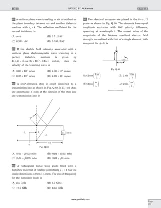

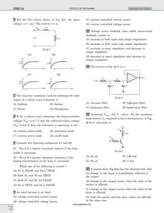
![14. The range of signed decimal numbers that can be
represented by 6-bit 1’s complement numbers is
(A) -31 to +31 (B) -63 to +64
(C) -64 to +63 (D) -32 to +31
15. A digital system is required to amplify a
binary-encoded audio signal. The user should be able to
control the gain of the amplifier from a minimum to a
maximum in 100 increments. The minimum number of
bits required to encode, in straight binary, is
(A) 8 (B) 6
(C) 5 (D) 7
16. Choose the correct one from among the alternatives
A, B, C, D after matching an item from Group 1 with
the most appropriate item in Group 2.
Group 1 Group 2
P: Shift register 1: Frequency division
Q: Counter 2: Addressing in memory chips
R: Decoder 3: Serial to parallel data conversion
(A) (B) (C) (D)
P–3 P–3 P–2 P–1
Q–2 Q–1 Q–1 Q–3
R–1 R–2 R–3 R–2
17. Fig. Q.17 shows the internal schematic of a TTL
AND-OR-Invert (AOI) gate. For the inputs shown in
Fig. Q.17, the output Y is
(A) 0 (B) 1
(C) AB (D) AB
18. Fig. Q.18 is the voltage transfer characteristic of
(A) an NMOS inverter with enhancement mode
transistor as load
(B) an NMOS inverter with depletion mode transistor
as load
(C) a CMOS inverter
(D) a BJT inverter
19. The impulse response h n[ ] of a linear time-invariant
system is given by
h n u n u n u n[ ] [ ] [ ] [ ]= + + - - -3 2 2 7
where u n[ ] is the unit step sequence. The above
system is
(A) stable but not causal
(B) stable and causal
(C) causal but unstable
(D) unstable and not causal
20. The distribution function F xX( ) of a random variable
X is shown in Fig. Q.20. The probability that X = 1 is
(A) zero (B) 0.25
(C) 0.55 (D) 0.30
21. The z-transform of a system is
H z
z
z
( )
.
=
- 0 2
If the ROC is | |z < 0.2, then the impulse response
of the system is
(A) ( . ) [ ]0 2 n
u n (B) ( . ) [ ]0 2 1n
u n- -
(C) -( . ) [ ]0 2 n
u n (D) - - -( . ) [ ]0 2 1n
u n
22. The Fourier transform of a conjugate symmetric
function is always
(A) imaginary (B) conjugate anti-symmetric
(C) real (D) conjugate symmetric
Chap 10.2
Page
605
EC-04
A
y
B
Input are
Floating
Fig Q.17
Vin
0
Vout
Fig Q.18
F xx( )
0 1
0.25
0.55
1.0
2
x
-2
Fig Q.20
GATE EC BY RK Kanodia
www.gatehelp.com](https://image.slidesharecdn.com/a-150815031147-lva1-app6892/85/A-gate-by-rk-kanodia-410-320.jpg)
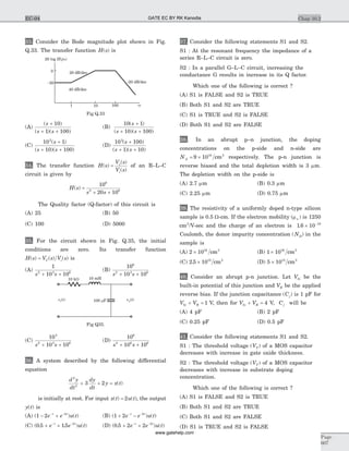
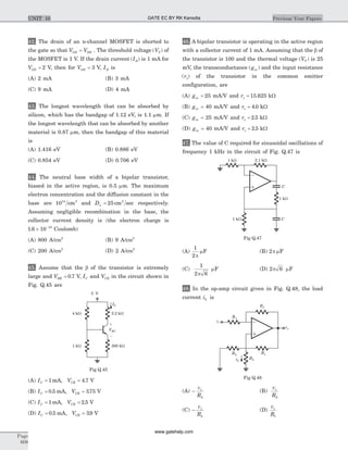
![57. Consider the sequence of 8085 instructions given
below
LXI H, 9258
MOV A, M
CMA
MOV M , A
Which one of the following is performed by this
sequence?
(A) Contents of location 9258 are moved to the
accumulator
(B) Contents of location 9258 are compared with the
contents of the accumulator
(C) Contents of location 8529 are complemented and
stored in location 8529
(D) Contents of location 5892 are complemented and
stored in location 5892
58. A Boolean function f of two variables x and y is
defined as follows :
f f f f( , ) ( , ) ( , ) ; ( , )0 0 0 1 1 1 1 1 0 0= = = =
Assuming complements of x and y are not
available, a minimum cost solution for realizing f
using only 2-input NOR gates and 2-input OR gates
(each having unit cost) would have a total cost of
(A) 1 unit (B) 4 units
(C) 3 units (D) 2 units
59. It is desired to multiply the numbers 0AH by 0BH
and store the result in the accumulator. The numbers
are available in registers B and C respectively. A part of
the 8085 program for this purpose is given below:
MVI A, 00H
LOOP: ––––––––––
–––––––––––
–––––––––––
HLT
END
The sequence of instructions to complete the
program would be
(A) JNZ LOOP, ADD B, DCR C
(B) ADD B, JNZ LOOP, DCR C
(C) DCR C, JNZ LOOP, ADD B
(D) ADD B, DCR C, JNZ LOOP
60. A 1 kHz sinusoidal signal is ideally sampled at 1500
samples /sec and the sampled signal is passed through
an ideal low-pass filter with cut-off frequency 800 Hz.
The output signal has the frequency
(A) zero Hz (B) 0.75 kHz
(C) 0.5 kHz (D) 0.25 kHz
61. A rectangular pulse train s t( ) as shown in Fig. Q.61
is convolved with the signal cos ( )2 3
4 10p ´ t . The
convolved signal will be a
(A) DC (B) 12 kHz sinusoid
(C) 8 kHz sinusoid (D) 14 kHz sinusoid
62. Consider the sequence
x n j j[ ] [ ]= - - +
4 5 1 2 5
The conjugate anti-symmetric part of the sequence is
(A) [- -4 2 5j . j2 4 2 5- j . ]
(B) [- j2 5. 1 j2.5]
(C) [- j2.5 j2 0]
(D) [-4 1 4]
63. A causal LTI system is described by the difference
equation
2 2 2 1y n y n x n x n[ ] [ ] [ ] [ ]= - - + -a b
The system is stable only if
(A) a b= <2 2,
(B) a b> >2 2,
(C) a < 2, any value of b
(D) b < 2, any value of a
64. A causal system having the transfer function
H s
s
( ) =
+
1
2
is excited with 10u t( ). The time at which the
output reaches 99% of its steady state value is
(A) 2.7 sec (B) 2.5 sec
(C) 2.3 sec (D) 2.1 sec
Page
610
Previous Year PapersUNIT 10
0
1
t
1 ms
s t( )
Fig Q.61
GATE EC BY RK Kanodia
www.gatehelp.com](https://image.slidesharecdn.com/a-150815031147-lva1-app6892/85/A-gate-by-rk-kanodia-413-320.jpg)
![65. The impulse response h n[ ] of a linear time invariant
system is given as
h n
n
n[ ]
,
,=
- = -
= -
ì
í
ï
î
ï
2 2 1 1
4 2 2 2
0 otherwise
If the input to the above system is the sequence
ej np 4
, then the output is
(A) 4 2 4
ej np
(B) 4 2 4
e j n- p
(C) 4 4
ej np
(D) -4 4
ej np
66. Let x t( ) and y t( ) with Fourier transforms F f( ) and
Y f( ) respectively be related as shown in Fig. Q.66. Then
Y f( ) is
(A) - -1
2
2 2
X f e j f
( ) p
(B) -
1
2
2 2
X f ej f
( ) p
(C) - X f ej f
( )2 2p
(D) - -
X f e j f
( )2 2p
67. A system has poles at 0.01 Hz, 1 Hz and 80 Hz;
zeros at 5 Hz, 100 Hz and 200 Hz. The approximate
phase of the system response at 20 Hz is
(A) –90° (B) 0°
(C) 90° (D) –180°
68. Consider the signal flow graph shown in Fig. Q.68.
The gain
x
x
5
1
is
(A)
1 - + +( )be cf dg
abcd
(B)
bedg
be cf dg1 - + +( )
(C)
abcd
be cf dg bedg1 - + + +( )
(D)
1 - + + +( )be cf dg bedg
abcd
69. If A =
-
-
é
ë
ê
ù
û
ú
2 2
1 3
, then sin At is
(A)
sin( ) sin( ) sin( ) sin( )
sin( ) sin(
- + - - - + -
- - + -
4 2 4 2
4
t t t t
t t t t) sin( ) sin( )2 4- + -
é
ë
ê
ù
û
ú
(B)
sin( ) sin( )
sin( ) sin( )
-
-
é
ë
ê
ù
û
ú
2 2
3
t t
t t
(C)
sin( ) sin( ) sin( ) sin( )
sin( ) sin( )
4 2 2 4 2
4 2
t t t t
t t
+ - - -
- - + sin( ) sin( )4t t+
é
ë
ê
ù
û
ú
(D)
cos( ) cos( ) cos( ) sin( )
cos( ) sin( )
- + - - -
- - + -
t t t t
t t
2 2 4 2
4 - +
é
ë
ê
ù
û
ú2 4cos( ) cos( )t t
70. The open-loop transfer function of a unity feedback
system is
G s
K
s s s s
( )
( )( )
=
+ + +2
2 3
The range of K for which the system is stable is
(A)
21
4
0> >K (B) 13 0> >K
(C)
21
4
< < ¥K (D) - < < ¥6 K
71. For the polynomial
P s s s s s s( ) = + + + + +5 4 3 2
2 2 3 15
the number of roots which lie in the right half of
the s-plane is
(A) 4 (B) 2
(C) 3 (D) 1
72. The state variable equations of a system are :
&x x x u1 1 23= - - = , &x x2 12= , y x u= +1
The system is
(A) controllable but not observable
(B) observable but not controllable
(C) neither controllable nor observable
(D) controllable and observable
73. Given A =
é
ë
ê
ù
û
ú
1 0
0 1
, the state transition matrix eAt
is
given by
(A)
0
0
e
e
t
t
-
-
é
ë
ê
ù
û
ú (B)
0
0
e
e
t
t
é
ë
ê
ù
û
ú
(C)
e
e
t
t
-
-
é
ë
ê
ù
û
ú
0
0
(D)
e
e
t
t
0
0
é
ë
ê
ù
û
ú
Chap 10.2
Page
611
EC-04
a b c 1d
e f g
x3x1 x2 x4 x5
Fig Q.68
0
t
x( )t
2-2
0 t
y( )t
1
-1
-2
Fig Q.66
GATE EC BY RK Kanodia
www.gatehelp.com](https://image.slidesharecdn.com/a-150815031147-lva1-app6892/85/A-gate-by-rk-kanodia-414-320.jpg)
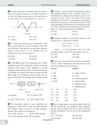
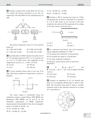

![19. The Boolean function f implemented in the figure
using two input multiplexes is
(A) ABC ABC+ (B) ABC ABC+
(C) ABC AB C+ (D) ABC ABC+
20. Which of the following can be impulse response of a
causal system?
(A) (B)
(C) (D)
21. Let x n u n y n x n
n
( ) ( ), ( ) ( )=
æ
è
ç
ö
ø
÷ =
1
2
2
and Y ej
( )w
be the
Fourier transform of y n( ) then Y ej
( )0
is
(A)
1
4
(B) 2
(C) 4 (D)
4
3
22. Find the correct match between group 1 and group 2
Group 1 Group II
P. { ( )} sin( )1 + km t A tcw W. Phase Modulation
Q. km t A tc( ) sin( )w X.Frequency Modulation
R. A t km tcsin( ( ))w + Y. Amplitude Modulation
(A) P-Z, Q-Y, R-X, S-W (B) P-W, Q-X, R-Y, S-Z
(C) P-X, Q-W, R-Z, S-Y (D) P-Y, Q-Z, R-W, S-X
23. The power in the signal
s t t( ) cos sin( )= -
æ
è
ç
ö
ø
÷ +8 20
2
4 15p
p
p is
(A) 40 (B) 41
(C) 42 (D) 82
24. Which of the following analog modulation scheme
requires the minimum transmitted power and
minimum channel bandwidth?
(A) VSB (B) DSB - SC
(C) SSB (D) AM
25. A linear system is equivalently represented by two
sets of state equations:
&X AX BU= + And &W CW DU= +
The eigenvalues of the representations are also
computed as [ ]l and [ ]m . Which one of the following
statements is true?
(A) [ ] [ ]l m= and X W= (B) [ ] [ ]l m= and X W¹
(C) [ ] [ ]l m¹ and X W= (D) [ ] [ ]l m= and X W¹
26. Which one of the following polar diagrams
corresponds to a lag network?
(A) (B)
(C) (D)
27. Despite the presence of negative feedback, control
systems still have problems of instability because the
(A) Components used have non-linearities
(B) Dynamic equations of the subsystem are not
known exactly.
(C) Mathematical analysis involves approximations.
(D) System has large negative phase angle at high
frequencies.
Chap 10.3
Page
617
EC-05
t t
h t( ) h t( )
h t( ) h t( )
t t Im
Rew ¥=w= 0
Im
Re
w ¥=w= 0
Im
Re
w ¥=
w= 0
Im
Re
w ¥= w= 0
C
B
A
C
f
1
0
1
0 MUX
MUX
Fig. Q19
GATE EC BY RK Kanodia
www.gatehelp.com](https://image.slidesharecdn.com/a-150815031147-lva1-app6892/85/A-gate-by-rk-kanodia-419-320.jpg)
![37. Given an orthogonal matrix
A =
- -
-
-
é
ë
ê
ê
ê
ê
ù
û
ú
ú
ú
ú
1 1 1 1
1 1 1 1
1 1 0 0
0 0 1 1
, [ ]AAT -1
is
(A)
1
4
1
4
1
2
1
2
0 0 0
0 0 0
0 0 0
0 0 0
é
ë
ê
ê
ê
ê
ù
û
ú
ú
ú
ú
(B)
1
2
1
2
1
2
1
2
0 0 0
0 0 0
0 0 0
0 0 0
é
ë
ê
ê
ê
ê
ù
û
ú
ú
ú
ú
(C)
1 0 0 0
0 1 0 0
0 0 1 0
0 0 0 1
é
ë
ê
ê
ê
ê
ù
û
ú
ú
ú
ú
(D)
1
4
1
4
1
4
1
4
0 0 0
0 0 0
0 0 0
0 0 0
é
ë
ê
ê
ê
ê
ù
û
ú
ú
ú
ú
38. For the circuit show in the figure, the instantaneous
current i ti( ) is
(A)
10 3
2
90Ð ° Amps. (B)
10 3
2
90Ð - ° Amps.
(C) 5 60Ð ° Amps (D) 5 60Ð - ° Amps
39. Impedance Z as shown in the given figure is
(A) j29 W (B) j9 W
(C) j19 W (D) j39 W
40. For the circuit shown in figure, Thevenin's voltage
and Thevenin's equivalent resistance at terminals a - b
is
(A) 5 V and 2 W (B) 7.5 V and 2.5 W
(C) 4 V and 2 W (D) 3 V and 2.5 W
41. If R R R R1 2 3= = = and R R3 11= . in the bridge
circuit shown in the figure, then the reading in the ideal
voltmeter connected between a and b is
(A) 0.238 V (B) 0.138 V
(C) -0.238 V (D) 1 V.
42. The h parameters of the circuit shown in the figure
are
(A)
0 1 0 1
0 1 0 3
. .
. .-
é
ë
ê
ù
û
ú (B)
10 1
1 0 05
-é
ë
ê
ù
û
ú.
(C)
30 20
20 20
é
ë
ê
ù
û
ú (D)
10 1
1 0 05-
é
ë
ê
ù
û
ú.
43. A square pulse of 3 volts amplitude is applied to C-R
circuit shown in the figure. The capacitor is initially
uncharged. The output voltage VO at time t = 2 sec is
(A) 3 V (B) -3 V
(C) 4 V (D) -4 V
44. A Silicon sample A is doped with 1018
atoms/cm3
of
boron. Another sample b of identical dimension is doped
with 1018
atoms/cm3
phosphorus. The ratio of electron to
Chap 10.3
Page
619
EC-05
j5 W
j2 W
j10 W
j10 W
j2 W
Fig. Q39
5 W
a
b
5 W 10 V0.5I1
Fig. Q40
i1
j2
3 W5 0 A
O 10 60 AO
-j2
~
~
Fig. Q38
R1
a b10 V
R2
R3
R4
V
Fig. Q41
10 W
20 W
I1 I2
V1
+
-
V2
+
-
Fig. Q42
1 kW
I1 I2
V1
+
-
V2
+
-
Vi
3 V
t
2 sec
0.1 Fm - 2j
Fig. Q43
GATE EC BY RK Kanodia
www.gatehelp.com](https://image.slidesharecdn.com/a-150815031147-lva1-app6892/85/A-gate-by-rk-kanodia-420-320.jpg)
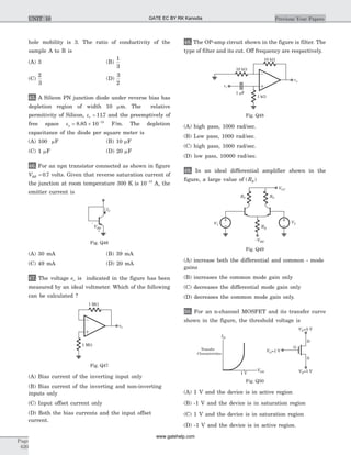
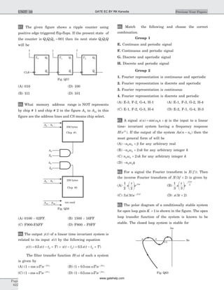
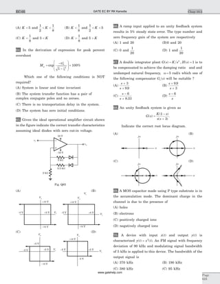
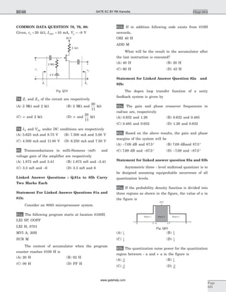
![Statement of Linked Answer Questions 84a and
84b
Voltage standing wave pattern in a lossless
transmission line with characteristic impedance 50 and
a resistive load is shown in the figure.
84a. The value of the load resistance is
(A) 50 W (B) 200 W
(C) 12 5. W (D) 0
84b. The reflection coefficient is given by
(A) -0 6. (B) -1
(C) 0.6 (D) 0
Statement of Linked Answer Question 85a and
85b:
A sequence x (n) has non-zero values as shown in
the figure.(A)
85a. The sequence
y n
x
n
n
n
[ ] =
-
æ
è
ç
ö
ø
÷
ì
í
ï
î
ï
2
1
0
for even
for odd
will be
85b. The Fourier transform of y n[ ]2 will be
(A) e j-
+ +2
4 2 2 2w
w w[cos cos ]
(B) [cos cos ]2 2 2w w+ +
(C) e j-
+ +w
w w[cos cos ]2 2 2
(D) e j-
+ +2
2 2 2w
w w[cos cos ]
************
Page
626
Previous Year PapersUNIT 10
1
½
y n[ ]
n
2 31 4 5 60-1-2-3-4-5-6
2
(B)
1
½
x n[ ]
n
2 31 4 5 60-1-2-3-4-5-6
2
Fig. Q85
1
½
y n[ ]
n
2 31 4 5 60-1-2-3-4-5-6
2
(A)
4
1
l/2l
V z( )
Fig. Q84a and Q84b
1
½
y n[ ]
n
2 31 4 5 60-1-2-3-4-5-6
2
-2
(C)
1
½
y n[ ]
n
2 31 4 5 60-1-2-3-4-5-6
2
(D)
GATE EC BY RK Kanodia
www.gatehelp.com](https://image.slidesharecdn.com/a-150815031147-lva1-app6892/85/A-gate-by-rk-kanodia-425-320.jpg)
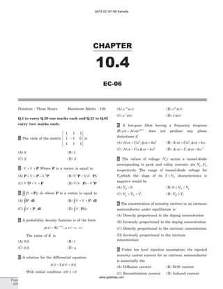
![10. The phenomenon known as “Early Effect” in a
bipolar transistor refers to a reduction of the effective
base-width caused by
(A) Electron – Hole recombination at the base
(B) The reverse biasing of the base – collector
junction
(C) The forward biasing of emitter-base junction
(D) The early removal of stored base charge during
saturation-to-cut off switching
11. The input impedance ( )Zi and the output impedance
( )Z0 of an ideal trans-conductance (voltage controlled
current source) amplifier are
(A) Z Zi = =0 00, (B) Z Zi = = ¥0 0,
(C) Z Zi = ¥ =, 0 0 (D) Z Zi = ¥ = ¥, 0
12. An n-channel depletion MOSFET has following two
points on its I VD GS- curve :
(i) V IGS D= =0 12at mA and
(ii) V IGS D= - =6 0Volts at mA
Which of the following Q – point will give the
highest trans – conductance gain for small signals?
(A) VGS = -6 Volts (B) VGS = -3 Volts
(C) VGS = 0 Volts (D) VGS = 3 Volts
13. The number of product terms in the minimized
sum-of-product expression obtained through the
following K – map is (where, “d” denotes don’t care
states)
1 0 0 1
0 d 0 0
0 0 d 1
1 0 0 1
(A) 2 (B) 3
(C) 4 (D) 5
14. Let x t X j( ) ( )« w be Fourier Transform pair. The
Fourier Transform of the signal x t( )5 3- in terms of
X j( )w is given as
(A)
1
5 5
3
5
e X
j
j
- æ
è
ç
ö
ø
÷
w
w
(B)
1
5 5
3
5
e X
j
j w
wæ
è
ç
ö
ø
÷
(C)
1
5 5
3
e X
jj- æ
è
ç
ö
ø
÷
w w
(D)
1
5 5
3
e X
jj w wæ
è
ç
ö
ø
÷
15. The Dirac delta function is defined as
(A) d( )t
t
=
=ì
í
î
1 0
0 otherwise
(B) d( )t
t
=
=ì
í
î
1 0
0 otherwise
(C) d( )t
t
=
=ì
í
î
1 0
0 otherwise
and d( )t dt
-¥
¥
ò = 1
(D) d( )t
t
=
¥ =ì
í
î
0
0 otherwise
and d( )t dt
-¥
¥
ò = 1
16. If the region of convergence of x n x n1 2[ ] [ ]+ is
1
3
2
3
< <z then the region of convergence of x n x n1 2[ ] [ ]-
includes
(A)
1
3
3< <z (B)
2
3
3< <z
(C)
3
2
3< <z (D)
1
3
2
3
< <z
17. The open-loop function of a unity-gain feedback
control system is given by
G s
K
s s
( )
( )( )
=
+ +1 2
The gain margin of the system in dB is given by
(A) 0 (B) 1
(C) 20 (D)
18. In the system shown below, x t t u t( ) (sin ) ( )= In
steady-state, the response y t( ) will be
(A)
1
2 4
sin t -
æ
è
ç
ö
ø
÷
p
(B)
1
2 4
sin t +
æ
è
ç
ö
ø
÷
p
(C)
1
2
e tt-
sin (D) sin cost t-
19. The electric field of an electromagnetic wave
propagation in the positive direction is given by
E a t z a t zx y= - + - +$ sin( ) $ sin( )w b w b p 2
The wave is
(A) Linearly polarized in the z–direction
(B) Elliptically polarized
(C) Left-hand circularly polarized
(D) Right-hand circularly polarized
Chap 10.4
Page
629
EC-06
x t( ) y t( )1
s + 1
Fig Q. 18
GATE EC BY RK Kanodia
www.gatehelp.com](https://image.slidesharecdn.com/a-150815031147-lva1-app6892/85/A-gate-by-rk-kanodia-427-320.jpg)


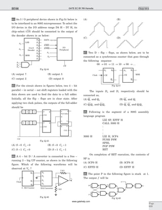
![(A)
p
2
(B)
p
3
(C)
p
4
(D)
p
6
59. A linear system is described by the following state
equation
& ( ) ( ) ( ),X t AX t BU t A= + =
-
é
ë
ê
ù
û
ú
0 1
1 0
The state transition matrix of the system is
(A)
cos sin
sin cos
t t
t t-
é
ë
ê
ù
û
ú (B)
-
- -
é
ë
ê
ù
û
ú
cos sin
sin cos
t t
t t
(C)
- -
-
é
ë
ê
ù
û
ú
cos sin
sin cos
t t
t t
(D)
- -é
ë
ê
ù
û
ú
cos sin
cos sin
t t
t t
60. The minimum step- size required for a Delta –
Modulator operating at 32 K , samples/sec to track the
signal (here u t( ) is the unit function)
x t t u t u t t u t u t( ) ( ( ) ( )( )( ( ) ( ))= - - - - - -125 1 250 125 1 2
So that slope overload is avoided, would be
(A) 2 10-
(B) 2 8-
(C) 2 6-
(D) 2 4-
61. A zero mean white Gaussian noise is passed
through an ideal lowpass filter of bandwidth 10 kHz.
The output is then uniformly sampled with sampling
period ts = 0 03. msec. The samples so obtained would be
(A) correlated (B) statistically independent
(C) uncorrelated (E) orthogonal
62. A source generates three symbols with probabilities
0.25, 0.25, 0.50 at a rate of 3000 symbols per second.
Assuming independent generation of symbols, the most
efficient source encoder would have average bit rate as
(A) 6000 bits/sec (B) 4500 bits/sec
(C) 3000 bits/sec (D) 1500 bits/sec
63. The diagonal clipping in Amplitude Demodulation
(using envelope detector) can be avoided if RC time –
constant of the envelope detector satisfies the following
condition, (here W is message bandwidth and wc is
carrier frequency both in rad /sec)
(A) RC
W
<
1
(B) RC
W
>
1
(C) RC
c
<
1
w
(D) RC
c
>
1
w
64. In the following figure the minimum value of the
constant “C” , which is to be added to y t1( ) and y t2( )
such that y t1( ) and y t2( ) and are different, is
(A) D (B)
D
2
(C)
D2
12
(D)
D
L
65. A message signal with 10 kHz bandwidth is lower
side Band SSB modulated with carrier fc1
6
10= Hz
frequency the resulting signal is then passed through a
Narow Band Frequency Modulator with carrier
frequency fc2
9
10= Hz. The bandwidth of the output
would be
(A) 4 104
´ Hz (B) 2 106
´ Hz
(C) 2 109
´ Hz (D) 2 1010
´ Hz
66. A medium of relative permitivity er2 2= forms an
interface with free – space. A point source of
electromagnetic energy is located in the medium at a
depth of 1 meter from the interface. Due to the total
internal reflection, the transmitted beam has a circular
cross-section over the interface. The area of the beam
cross-section at the interface is given by
(A) 2 2
p m (B) p2 2
m
(C) p
2
2
m (D) p m2
67. A medium is divide into regions I and II about x = 0
plane, as shown in the figure below. An electromagnetic
wave with electric field E a a ax y z1 4 3 5= + +$ $ $ is incident
normally on the interface from region I. The electric file
E2 in region II at the interface is
Chap 10.4
Page
635
EC-06
C
x( ) with ranget
Q is quantizer with levels,
stepwise allowable signal
dynamic range [ , V]
L
V
D
-
y t1( )
y t2( )
QQ-V
2
, V
2
Fig Q.64
m m
s
2
2
=
=4
=0
o
re
2
m m
s
1
1
=
=4
=0
o
re
1
Region IIRegion I
x < 0 x > 0x = 0
E2E1
Fig Q.67
GATE EC BY RK Kanodia
www.gatehelp.com](https://image.slidesharecdn.com/a-150815031147-lva1-app6892/85/A-gate-by-rk-kanodia-431-320.jpg)
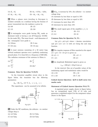
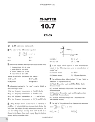
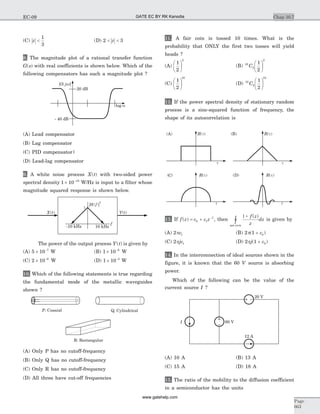
![(A) V -1
(B) cm. -1
V
(C) V.cm-1
(D) V.s
16. In a microprocessor, the service routine for a certain
interrupt starts from a fixed location of memory which
cannot be externally set, but the interrupt can be
delayed or rejected Such an interrupt is
(A) non-maskable and non-vectored
(B) maskable and non-vectored
(C) non-maskable and vectored
(D) maskable and vectored
17. If the transfer function of the following network is
V s
V si
0( )
( )
=
+
1
2 sCR
the value of the load resistance RL is
(A) R/4 (B) R/2
(C) R (D) 2 R
18. Consider the system
dx
dt
Ax Bu= + with A =
é
ë
ê
ù
û
ú
1 0
0 1
and B
p
q
=
é
ë
ê
ù
û
ú where p and q are arbitrary real numbers.
Which of the following statements about the
controllability of the system is true ?
(A) The system is completely state controllable for
any nonzero values of p and q
(B) Only p = 0 and q = 0 result in controllability
(C) The system is uncontrollable for all values of p
and q
(D) We cannot conclude about controllability from the
given data
19. For a message signal m t f tm( ) cos( )= 2p and carrier of
frequency fc, which of the following represents a single
side-band (SSB) signal ?
(A) cos( )cos( )2 2p pf t f tm c
(B) cos( )2pf tc
(C) cos[ ( ) ]2p f f tc m+
(D) [ cos( )cos( )]1 2 2+ p pf t f tm c
20. Two infinitely long wires carrying current are as
shown in the figure below. One wire is in the y z- plane
and parallel to the y -axis. The other wire is in the x y-
plane and parallel to the x -axis. Which components of
the resulting magnetic field are non-zero at the origin ?
(A) x y z, , components (B) x y, components
(C) y z, components (D) x z, components
Q. 21 to Q. 60 carry two marks each.
21. Consider two independent random variables X and
Y with identical distributions. The variables X and Y
take values 0, 1 and 2 with probabilities
1
2
1
4
, and
1
4
respectively. What is the conditional probability
P X Y X Y( )+ = - =2 0 ?
(A) 0 (B)
1
16
(C)
1
6
(D) 1
22. The Taylor series expansion of
sin x
x - p
at x = p is given
by
(A) 1
3
2
+
-
+
( )
!
...
x p
(B) - -
-
+1
3
2
( )
!
...
x p
(C) 1
3
2
-
-
+
( )
!
...
x p
(D) - +
-
+1
3
2
( )
!
...
x p
23. If a vector field V
®
is related to another vector field A
®
through V A
® ®
= Ñ ´ , which of the following is true? Note :
C and SC refer to any closed contour and any surface
whose boundary is C.
(A) V dl
C
® ®
ò . =
® ®
òò A dS
SC
. (B) A dl
C
® ®
ò . =
® ®
òòV dS
SC
.
(C) Ñ ´
® ®
ò V dl
C
. = Ñ ´
® ®
òò A dS
SC
. (D) Ñ ´ò
® ®
C
A dl. =
® ®
òòV dS
SC
.
Page
664
Previous year PapersUNIT 10
–
+
–
+
x
y
z 1 A
1 A
GATE EC BY RK Kanodia
www.gatehelp.com](https://image.slidesharecdn.com/a-150815031147-lva1-app6892/85/A-gate-by-rk-kanodia-436-320.jpg)
![24. Given that F s( ) is the one-sided Laplace transform
of f t( ), the Laplace transform of f d
t
( )t t
0ò is
(A) sF s f( ) ( )- 0 (B)
1
s
F s( )
(C) F d
s
( )t t
0ò (D)
1
0
s
F s f[ ( ) ( )]-
25. Match each differential equation in Group I to its
family of solution curves from Group II.
Group 1 Group II
P.
dy
dx
y
x
= 1. Circles
Q.
dy
dx
y
x
= - 2. Straight lines
R.
dy
dx
x
y
= 3. Hyperbolas
S.
dy
dx
x
y
= -
(A) P Q R S- - - -2 3 3 1, , ,
(B) P Q R S- - - -1 3 2 1, , ,
(C) P Q R S- - - -2 1 3 3, , ,
(D) P Q R S- - - -3 2 1 2, , ,
26. The eigen values of the following matrix are
-
- -
é
ë
ê
ê
ê
ù
û
ú
ú
ú
1 3 5
3 1 6
0 0 3
(A) 3 3 5 6, ,+ -j j (B) - + + -6 5 3 3j j j, ,
(C) 3 3 5+ - +j j j, , (D) 3 1 3 1 3, ,- + - -j j
27. An AC source of RMS voltage 20 V with internal
impedance Z js = +( )1 2 W feeds a load of impedance
Z jL = +( )7 4 W in the figure below. The reactive power
consumed by the load is
(A) 8 VAR (B) 16 VAR|
(C) 28 VAR (D) 32 VAR
28. The switch in the circuit shown was on position a
for a long time, and is move to position b at time t = 0.
The current i t( ) for t > 0 is given by
(A) 0 2 125
. ( )e u tt-
mA (B) 20 1250
e u tt-
( ) mA
(C) 0 2 1250
. ( )e u tt-
mA (D) 20 1000
e u tt-
( ) mA
29. In the circuit shown, what value of RL maximizes
the power delivered to RL ?
(A) 2.4 W (B)
8
3
W
(C) 4 W (D) 6 W
30. The time domain behavior of an RL circuit is
represented by
L
di
dt
Ri+ = + -
V Be t u tRt L
0 1( sin ) ( )/
.
For an initial current of i
V
R
( )0 0
= , the steady state
value of the current is given by
(A) i t
V
R
( ) ® 0
(B) i t
V
R
( ) ®
2 0
(C) i t
V
R
B( ) ( )® +0
1 (D) i t
V
R
B( ) ( )® +
2
10
31. In the circuit below, the diode is ideal. The voltage V
is given by
(A) min( , )Vi 1 (B) max( )Vi1
(C) min( , )-Vi 1 (C) max( , )-Vi 1
Chap 10.7
Page
665
EC-09
100 V
100 V
1 A
GATE EC BY RK Kanodia
www.gatehelp.com](https://image.slidesharecdn.com/a-150815031147-lva1-app6892/85/A-gate-by-rk-kanodia-437-320.jpg)
![(A) NAND: first (0,1) then (0,1) NOR: first (1,0) then
(0,0)
(B) NAND: first (1,0) then (1,0) NOR: first (1,0) then
(1,0)
(C) NAND: first (1,0) then (1,0) NOR: first (1,0) then
(0,0)
(D) NAND: first (1,0) then (1,1) NOR: first (0,1) then
(0,1)
39. What are the counting states ( , )Q Q1 2 for the counter
shown in the figure below?
(A) 11, 10, 00, 11, 10,... (B) 01, 10, 11, 00, 01,...
(C) 00, 11, 01, 10, 00,... (D) 01, 10, 00, 01, 10,...
40. A system with transfer function H z( ) has impulse
response h(.) defined as h( )2 1= , h( )3 1= - and h k( ) = 0
otherwise. Consider the following statements.
S1: H z( ) is a low-pass filter.
S2: H z( ) is an FIR filter.
Which of the following is correct?
(A) Only S2 is true
(B) Both S1 and S2 are false
(C) Both S1 and S2 are true, and S2 is a reason for
S1
(D) Both S1 and S2 are true, but S2 is not a reason
for S1
41. Consider a system whose input x and output y are
related by the equation
y t( )= -
-¥
¥
ò x t h d( ) ( )t t t2
where h t( ) is shown in the graph.
Which of the following four properties are
possessed by the system ?
BIBO: Bounded input gives a bounded output.
Causal: The system is causal,
LP: The system is low pass.
LTI: The system is linear and time-invariant.
(
A) Causal, LP (B) BIBO, LTI
(C) BIBO, Causal, LTI (D) LP, LTI
42. The 4-point Discrete Fourier Transform (DFT) of a
discrete time sequence {1,0,2,3} is
(A) [0,-2+2j,2,-2-2j] (B) [2,2+2j,6,2-2j]
(C) [6,1-3j,2,1+3j] (D) [6-1+3j,0,-1,-3j]
43. The feedback configuration and the pole-zero
locations of G s( ) =
- +
+ +
s s
s s
2
2
2 2
2 2
are shown below. The root
locus for negative values of k, i.e. for -¥ < <k 0, has
breakaway/break-in points and angle of departure at
pole P (with respect to the positive real axis) equal to
(A) ± 2 and 0° (B) ± 2 and 45°
(C) ± 3 and 0° (D) ± 3 and 45°
44. An LTI system having transfer function
s
s s
2
2
1
2 1
+
+ +
and input x t t( ) sin( )= + 1 is in steady state. The output
is sampled at a rate ws rad/s to obtain the final output
{ ( )}x k . Which of the following is true?
(A) y(.) is zero for all sampling frequencies ws
(B) y(.) is nonzero for all sampling frequencies ws
(C) y(.) is nonzero for ws > 2, but zero for ws < 2
(D) y(.) is zero for ws > 2, but nonzero for w2 2<
45. The unit step response of an under-damped second
order system has steady state value of -2. Which one of
the following transfer functions has these properties ?
(A)
-
+ +
2 24
2 59 1122
.
. .s s
(B)
-
+ +
3 82
191 1912
.
. .s s
(C)
-
- +
2 24
2 59 1122
.
. .s s
(D)
-
- +
382
191 1912
s s. .
Chap 10.7
Page
667
EC-09
Clock
K
Q
1
Q
Q
JK
Flip Flop
JK
Flip Flop
0
+
+
-
k G(s)
Im (s)
Re (s)
Q
O X
P
GATE EC BY RK Kanodia
www.gatehelp.com](https://image.slidesharecdn.com/a-150815031147-lva1-app6892/85/A-gate-by-rk-kanodia-438-320.jpg)
![46. A discrete random variable X takes values from 1 to
5 with probabilities as shown in the table. A student
calculates the mean of X as 3.5 and her teacher
calculates the variance of X as 1.5. Which of the
following statements is true ?
k 1 2 3 4 5
P X k( )= 0.1 0.2 0.4 0.2 0.1
(A) Both the student and the teacher are right
(B) Both the student and the teacher are wrong
(C) The student is wrong but the teacher is right
(D) The student is right but the teacher is wrong
Q. 47 A message signal given by
1n t( )=
æ
è
ç
ö
ø
÷ -
æ
è
ç
ö
ø
÷
1
2
1
2
1 2cos sinw wt t
is amplitude-modulated with a carrier of frequency
wc to generate
s t( )= +[ ( )]cos1 m t tcw
What is the power efficiency achieved by this
modulation scheme ?
(A) 8.33% (B) 11.11%
(C) 20% (D) 25%
48. A communication channel with AWGN operating at
a signal to noise ratio SNR >> 1 and bandwidth B has
capacity C1. If the SNR is doubled keeping B constant,
the resulting capacity C2 is given by
(A) C C2 12= (B) C C B2 1= +
(C) C C B2 1 2= + (D) C C B2 1 0 3= + .
49. A magnetic field in air is measured to be
B
®
=
+
-
+
æ
è
çç
ö
ø
÷÷B
x
x y
y
y
x y
x0 2 2 2 2
$ $
What current distribution leads to this field ?
[ Hint : The algebra is trivial in cylindrical coordinates.]
(A) j
B z
x y
®
=
+
æ
è
çç
ö
ø
÷÷
0
0
2 2
1$
,
m
r ¹ 0
(B) j
B z
x y
®
= -
+
æ
è
çç
ö
ø
÷÷
0
0
2 2
2$
,
m
r ¹ 0
(C) j
®
= 0, r ¹ 0
(D) j
B z
x y
®
=
+
æ
è
çç
ö
ø
÷÷
0
0
2 2
1$
,
m
r ¹ 0
50. A transmission line terminates in two branches,
each of length l / 4, as shown. The branches are
terminated by 50W loads. The lines are lossless and
have the characteristic impedances shown. Determine
the impedance Zi as seen by the source.
(A) 200W (B) 100W
(C) 50W (D) 25W
Common Date Questions
Common Date for Questions 51 and 52:
Consider a silicon p-n junction at room
temperature having the following parameters:
Doping on the n-side = ´1 1017
cm-3
Depletion width on the n-side = 0 1. mm
Depletion width on the p-side = 10. mm
Intrinsic carrier concentration = ´1 4 1010
. cm-3
Thermal voltage = 26 mV
Permittivity of free space = ´ -
8 85 10 14
. F.cm-1
Dielectric constant of silicon = 12
51 The built-in potential of the junction
(A) is 0.70 V
(B) is 0.76 V
(C) is 0.82
(D) cannot be estimated from the data given
52. The peak electric field in the device is
(A) 0.15 MV . cm-1
, directed from p-region to n-region
(B) 0.15 MV . cm-1
, directed from n-region to p-region
(C) 1.80 MV . cm-1
, directed from p-region to n-region
(D) 1.80 MV . cm-1
, directed from n-region to p-region
Common Data for Questions 53 and 54:
Page
668
Previous year PapersUNIT 10 GATE EC BY RK Kanodia
www.gatehelp.com](https://image.slidesharecdn.com/a-150815031147-lva1-app6892/85/A-gate-by-rk-kanodia-439-320.jpg)
![The Nyquist plot of a stable transfer function G s( )
is shown in the figure. We are interested in the stability
of the closed loop system in the feedback configuration
shown.
53. Which of the following statements is true?
(A) G s( ) is an all-pass filter
(B) G s( ) has a zero in the right-half plane
(C) G s( ) is the impedance of a passive network
(D) G s( ) is marginally stable
54. The gain and phase margins of G s( ) for closed loop
stability are
(A) 6 dB and 180° (B) 3 dB and 180°
(C) 6 dB and 90° (D) 3 dB and 90°
Common Data for Questions 55 and 56:
The amplitude of a random signal is uniformly
distributed between -5 V and 5 V.
55. If the signal to quantization noise ratio required in
uniformly quantizing the signal is 43.5 dB, the step size
of the quantization is approximately
(A) 0.0333 V (B) 0.05 V
(C) 0.0667 V (D) 0.10 V
56. If the positive values of the signal are uniformly
quantized with a step size of 0.05 V, and the negative
values are uniformly quantized with a step size of 0.1 V,
the resulting signal to quantization noise ratio is
approximately
(A) 46 dB (B) 43.8 dB
(C) 42 dB (D) 40 dB
Linked Answer Questions
Statement for Linked Answer Questions 57 and 58
:
Consider the CMOS circuit shown, where the gate
voltage VG of the n-MOSFET is increased from zero,
while the gate voltage of the p-MOSFET is kept
constant at 3 V. Assume that, for both transistors, the
magnitude of the threshold voltage is 1 V and the
product of the trans-conductance parameter and the
(W/L) ratio, i.e. the quantity mC W Lax ( / ), is 1 mA . V -2
.
57. For small increase in VG beyond 1 V, which of the
following gives the correct description of the region of
operation of each MOSFET ?
(A) Both the MOSFETs are in saturation region
(B) Both the MOSFETs are in triode region
(C) n-MOSFET is in triode and p-MOSFET is in
saturation region
(D) n-MOSFET is in saturation and p-MOSFET is in
triode region.
58. Estimate the output voltage V0 for V VG = 15. .
[Hint : Use the appropriate current-voltage equation for
each MOSFET, based on the anser to Q. 57.]
Statement for Linked Answer Questions 59 and
60:
Two products are sold from a vending machine,
which has two push buttons P1 and P2. When a button is
pressed, the price of the corresponding product is
displayed in a 7-segment display.
If no buttons are pressed, '0' is displayed,
signifying 'Rs. 0'.
If only P1 is pressed, '2' is displayed, signifying 'Rs.
2'.
If only P2 is pressed, '5' is displayed, signifying 'Rs.
5'.
If both P1 and P2 are pressed, 'E' is displayed,
signifying 'Error'.
Chap 10.7
Page
669
EC-09
+
+
-
G(s)
-1-0.5
Im
Re
-j
GATE EC BY RK Kanodia
www.gatehelp.com](https://image.slidesharecdn.com/a-150815031147-lva1-app6892/85/A-gate-by-rk-kanodia-440-320.jpg)

This document contains a sample multiple choice question (MCQ) exam for electronics and communication engineering. It includes 15 sample questions related to basic electrical concepts such as current, voltage, resistance, capacitance and circuits. It also provides the solutions and explanations for each question. The document is from a book titled "GATE EC by RK Kanodia" which is intended to help students prepare for the graduate aptitude test in engineering exam for electronics and communication.


![Lecture 1a [compatibility mode]](https://cdn.slidesharecdn.com/ss_thumbnails/lecture1acompatibilitymode-130523045820-phpapp02-thumbnail.jpg?width=640&height=640&fit=bounds)