This document provides solved problems from GATE (Graduate Aptitude Test in Engineering) exams from 1996-2013 in the subject of Engineering Mathematics. It contains one-mark and two-mark questions related to topics like differential equations, matrices, probability, complex analysis etc. along with their solutions. The document is available for purchase in digital format at www.nodia.co.in in separate sections or 'units'.


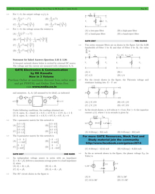
![GATE Electronics and Communication Topicwise Solved Paper by RK Kanodia & Ashish Murolia Page 1
d y t
dy t
2 y t 2
dy
=- =
dy
SPECIAL EDITION ( STUDY MATERIAL FORM )
At market Book is available in 3 volume i.e. in 3 book binding
form. But at NODIA Online Store book is available in 10 book
binding form. Each unit of Book is in separate binding.
Available Only at NODIA Online Store
Click to Buy
www.nodia.co.in
UNIT 1
ENGINEERING MATHEMATICS
2013 ONE MARK
1.1 The maximum value of q until which the approximation sinq . q
holds to within 10% error is
(A) 10c (B) 18c
(C) 50c (D) 90c
1.2 The minimum eigen value of the following matrix is
3
5
2
5
12
7
2
7
5
R
SSSS
T
V
WWWW
X
(A) 0 (B) 1
(C) 2 (D) 3
4
1.3 A polynomial f (x) a4x a 3
x a x a x a
3
2
2
= + + + 1 - 0 with all coefficients
positive has
(A) no real roots
(B) no negative real root
(C) odd number of real roots
(D) at least one positive and one negative real root
2013 TWO MARKS
1.4 Let A be an m#n matrix and B an n#m matrix. It is given that
determinant ^Im + ABh = determinant ^In + BAh, where Ik is the
k#k identity matrix. Using the above property, the determinant of
the matrix given below is
2
1
1
1
1
2
1
1
1
1
2
1
1
1
1
2
R
SSSSS
S
T
V
WWWWW
W
X
(A) 2 (B) 5
(C) 8 (D) 16
2012 ONE MARK
1.5 With initial condition x(1) = 0.5, the solution of the differential
equation
t dt
dx + x = t , is
(A) x t 2
= - 1 (B) x = t 2- 1
2
= (D) x t2
(C) x t
2
2
=
= 1
2 + - + .
1.6 Given f (z) z 1 z
3
If C is a counter clockwise path in the z -plane such that
z + 1 = 1, the value of 1
2 j f (z)dz
C p # is
(A) -2 (B) -1
(C) 1 (D) 2
1.7 If x = -1, then the value of xx is
(A) e-p/2 (B) ep/2
(C) x (D) 1
2012 TWO MARKS
1.8 Consider the differential equation
( ) ( )
( )
dt
dt
2
+ + = d(t)
with y(t) 2 and dt 0
t
t
0
0
=
=
-
-
The numerical value of dt
t=0+
is
(A) -2 (B) -1
(C) 0 (D) 1
1.9 The direction of vector A is radially outward from the origin, with
A = krn . where r2 = x2+ y2+ z2 and k is a constant. The value of
n for which d:A = 0 is
(A) -2 (B) 2
(C) 1 (D) 0
1.10 A fair coin is tossed till a head appears for the first time. The
probability that the number of required tosses is odd, is
(A) 1/3 (B) 1/2
(C) 2/3 (D) 3/4
1.11 The maximum value of f (x) = x3- 9x2+ 24x + 5 in the interval [1,6]
is
(A) 21 (B) 25
(C) 41 (D) 46
1.12 Given that
- -
> H = > H, the value of A3 is
5
2
3
0
A and I
1
0
0
= 1
(A) 15A+ 12I (B) 19A+ 30I
(C) 17A+ 15I (D) 17A+ 21I
2011 ONE MARK
1.13 Consider a closed surface S surrounding volume V . If rv is the
position vector of a point inside S , with nt the unit normal on S ,
the value of the integral 5r n dS
## v $ t is
S
(A) 3V (B) 5V
(C) 10V (D) 15V
dy = ky y = c is
1.14 The solution of the differential equation dx , (0)
(A) x = ce-ky (B) x = kecy
(C) y = cekx (D) y = ce-kx
1.15 The value of the integral
# - + where c is the circle
z dz
4 5
3 4
(z z )
c
2+ +
z = 1 is given by
(A) 0 (B) 1/10
(C) 4/5 (D) 1](https://image.slidesharecdn.com/kanodiamuroliapreviousyears-141121003216-conversion-gate02/85/Kanodia-murolia-previousyears-2-320.jpg)

![GATE Electronics and Communication Topicwise Solved Paper by RK Kanodia & Ashish Murolia Page 4
GATE Electronics & Communication
by RK Kanodia
Now in 3 Volume
Purchase Online at maximum discount from online store
and get POSTAL and Online Test Series Free
visit www.nodia.co.in
2 - # is
ds
1
1
For more GATE Resources, Mock Test and
Study material join the community
http://www.facebook.com/gateec2014
(C) is 1
(D) depends on the direction (clockwise or anit-clockwise) of the
semicircle
2007 ONE MARK
1.46 The following plot shows a function which varies linearly with x .
The value of the integral I ydx
1
2
= # is
(A) 1.0 (B) 2.5
(C) 4.0 (D) 5.0
1.47 For x << 1, coth (x) can be approximated as
(A) x (B) x2
(C)
1 (D)
x
1
2
x
sin 2
0 q
1.48 lim
q
q"
b l
is
(A) 0.5 (B) 1
(C) 2 (D) not defined
1.49 Which one of following functions is strictly bounded?
(A) 1/x2 (B) ex
(C) x2 (D) e x- 2
1.50 For the function e x - , the linear approximation around x = 2 is
(A) (3 - x)e-2 (B) 1 - x
(C) 63 + 3 2 - (1 - 2)x @e-2 (D) e-2
2007 TWO MARKS
1.51 The solution of the differential equation k
2 d y y y
dx
2
2
= - 2 under the
boundary conditions
(i) y = y1 at x = 0 and
(ii) y = y2 at x = 3, where k,y1 and y2 are constants, is
x y = 1- 2 a- 2 k+ 2 (B) y (y y )exp k
(A) y (y y )exp
k
x y = 2- 1 a- k+ 1
x y = ^ 1- 2h a k+ 1 (D) y y y exp k
(C) y y y sinh k
x y = ^ 1- 2h a- k+ 2
1.52 The equation x3- x2+ 4x - 4 = 0 is to be solved using the Newton
- Raphson method. If x = 2 is taken as the initial approximation of
the solution, then next approximation using this method will be
(A) 2/3 (B) 4/3
(C) 1 (D) 3/2
1.53 Three functions f1(t), f2(t) and f3(t) which are zero outside the interval
[0, T] are shown in the figure. Which of the following statements is
correct?
(A) f1(t) and f2(t) are orthogonal
(B) f1(t) and f3(t) are orthogonal
(C) f2(t) and f3(t) are orthogonal
D) f1(t) and f2(t) are orthonormal
1.54 If the semi-circular control D of radius 2 is as shown in the figure,
then the value of the integral
(s )
D
(A) jp (B) -jp
(C) -p (D) p
1.55 It is given that , ... X X XM
1 2 at M non-zero, orthogonal vectors.
The dimension of the vector space spanned by the 2M vectors
X1,X2,...XM, - X1, - X2,... - XM is
(A) 2M (B) M+ 1
(C) M
(D) dependent on the choice of , ,... X X XM
1 2
1.56 Consider the function f (x) = x2- x - 2. The maximum value of f (x)
in the closed interval [- 4, 4] is
(A) 18 (B) 10
(C) -225 (D) indeterminate
1.57 An examination consists of two papers, Paper 1 and Paper 2. The
probability of failing in Paper 1 is 0.3 and that in Paper 2 is 0.2.
Given that a student has failed in Paper 2, the probability of failing
in Paper 1 is 0.6. The probability of a student failing in both the
papers is
(A) 0.5 (B) 0.18
(C) 0.12 (D) 0.06](https://image.slidesharecdn.com/kanodiamuroliapreviousyears-141121003216-conversion-gate02/85/Kanodia-murolia-previousyears-5-320.jpg)
![GATE Electronics and Communication Topicwise Solved Paper by RK Kanodia & Ashish Murolia Page 7
SSSSS
S
WWWWW
W
R
SSSSS
S
SSSSS
S
WWWWW
W
WWWWW
W
SSSSS
S
WWWWW
W
SSSSS
S
WWWWW
W
SPECIAL EDITION ( STUDY MATERIAL FORM )
At market Book is available in 3 volume i.e. in 3 book binding
form. But at NODIA Online Store book is available in 10 book
binding form. Each unit of Book is in separate binding.
Available Only at NODIA Online Store
Click to Buy
www.nodia.co.in
SOLUTIONS
1.1 Option (B) is correct.
Here, as we know
Limsin
0
q
q"
. 0
but for 10% error, we can check option (B) first,
= = p =
q 18 18 .
c c# 0 314
180
c
sinq = sin18c = 0.309
= 0 314 - 0 309 #100 = 0 49
. . % . % 0 309
% error .
Now, we check it for q = 50c
= = p =
q 50 50 .
c c# 0 873
180
c
sinq = sin50c = 0.77
0.77 0.873 . % = 0 873 12 25 - =-
% error .
so, the error is more than 10%. Hence, for error less than 10%,
q = 18c can have the approximation
sin q . q
1.2 Option (A) is correct.
For, a given matrix A 6 @ the eigen value is calculated as
A - lI = 0
where l gives the eigen values of matrix. Here, the minimum eigen
value among the given options is
l = 0
We check the characteristic equation of matrix for this eigen value
A - lI = A (for l = 0)
3
5
2
5
12
7
2
7
5
=
= 3^60 - 49h- 5^25 - 14h+ 2^35 - 24h
= 33 - 55 + 22
= 0
Hence, it satisfied the characteristic equation and so, the minimum
eigen value is
l = 0
1.3 Option (D) is correct.
Given, the polynomial
f^xh a4x 4
a x 3
a x 2
3
2
a x a
= + + + 1 - 0
Since, all the coefficients are positive so, the roots of equation is
given by
f^xh = 0
It will have at least one pole in right hand plane as there will be
least one sign change from ^a1h to ^a0h in the Routh matrix 1st col-umn.
Also, there will be a corresponding pole in left hand plane
i.e.; at least one positive root (in R.H.P)
and at least one negative root (in L.H.P)
Rest of the roots will be either on imaginary axis or in L.H.P
1.4 Option (B) is correct.
Consider the given matrix be
Im + AB
2
1
1
1
1
2
1
1
1
1
2
1
1
1
1
2
=
R
T
V
X
where m = 4 so, we obtain
AB
2
1
1
1
1
2
1
1
1
1
2
1
1
1
1
2
1
0
0
0
0
1
0
0
0
0
1
0
0
0
0
1
= -
T
R
T
V
X
V
X
1
1
1
1
1
1
1
1
1
1
1
1
1
1
1
1
=
R
T
V
X
1
1
1
1
=
R
T
V
X
61 1 1 1@
Hence, we get
A
1
1
1
1
=
R
SSSSS
S
T
V
WWWWW
W
X
, B = 81 1 1 1B
R
Therefore, BA = 81 1 1 1B 1
SSSSS
WWWWW
1
1
1
S
T
V
W
X
= 4
From the given property
Det ^Im + ABh = Det^Im + BAh
& Det
2
1
1
1
1
2
1
1
1
1
2
1
1
1
1
2
R
SSSSS
S
T
V
WWWWW
W
X
Det
R
1
0
0
0
0
1
0
0
0
0
1
0
0
0
0
1
SSSSS
WWWWW
]]
]]
= + 4
S
T
V
W
X
Z
[
_
bb
bb
`
a
= 1 + 4
= 5
Note : Determinant of identity matrix is always 1.
1.5 Option (D) is correct.
dx + x = t
t dt
dx
dt
t x
+ = 1
dx + Px = Q (General form)
dt
1dt = # = # = =
Integrating factor, IF e Pdt e t elnt t
Solution has the form,
x#IF = # ^Q#IFhdt + C
x#t = # (1) (t)dt + C](https://image.slidesharecdn.com/kanodiamuroliapreviousyears-141121003216-conversion-gate02/85/Kanodia-murolia-previousyears-8-320.jpg)
![GATE Electronics and Communication Topicwise Solved Paper by RK Kanodia & Ashish Murolia Page 8
2
2
= x t2
1
1
C p # = sum of the residues of the poles which lie
- +
z
1 3
= 1 + +
z z
1 1
( )( )
= + +
GATE Electronics & Communication
by RK Kanodia
Now in 3 Volume
Purchase Online at maximum discount from online store
and get POSTAL and Online Test Series Free
visit www.nodia.co.in
dy t
dy
1 r A
2 r
1 krn
2
= 2 = 2 ( +
)
k n 2 rn
2
= + +1
= k(n + 2)rn-1 = 0 (given)
1
1
3 1 5
= +b l +b l +
2
1
1
df x
d f x
d f x
For more GATE Resources, Mock Test and
Study material join the community
http://www.facebook.com/gateec2014
xt = t2 +
C
Taking the initial condition,
x(1) = 0.5
0.5 2 C
= 1 + & C = 0
So, xt t
2
& =
1.6 Option (C) is correct.
f (z) z 1 z
3
= 2 + - +
2 j f (z)dz
inside the given closed region.
C & z + 1 = 1
Only pole z =- 1 inside the circle, so residue at z =- 1 is.
f (z)
(z ) (z )
( )( )
lim
z z
1 3
2 2
1
z 1
+ - + = =
"-
1
C p # = 1
So 2 j f (z)dz
1.7 Option (A) is correct.
= p + p
x = -1 = i cos 2 i sin 2
So, x = ei 2p
= 2p ^ h & ei i
xx ei x
^ h = e 2-p
2 p
1.8 Option (D) is correct.
d y t
dy t
( ) ( )
( )
dt
dt
y t
2
2
2
+ + = d(t)
By taking Laplace transform with initial conditions
0 dy 2 sy s y 0 Y s
- - + - +
; E = 1
s Y(s) sy( ) dt [ ( ) ( )] ( )
t
2
0
=
& 6s2Y(s) + 2s - 0@+ 26sY(s) + 2@+ Y(s) = 1
Y(s) [s2+ 2s + 1] = 1 - 2s - 4
Y(s)
- -
s
2 1
2 3
2 =
+ +
s s
We know that, If, y(t) Y(s) L
then,
dy t
( )
dt
sY(s) y(0) L -
So, sY(s) - y(0)
- - +
s s
2 1
( 2 3
)
s s
2 2 =
+ +
( )
2 2
- - + + +
s s s s
2 3 2 4 2
(s 2 s 1
)
2
=
+ +
sY(s) - y(0)
s
s
+ 1
+
+ =
(s 1 ) ( s
) ( s
)
2
1
1
1
2 2 2 =
+
+
+
1
s 1 (s 1
)
1
2 = + +
+
Taking inverse Laplace transform
( )
dt
= e-tu(t) + te-tu(t)
At t = 0+, dt
t=0+
= e0+ 0 = 1
1.9 Option (A) is correct.
Divergence of A in spherical coordinates is given as
d:A ( )
r r
2
2
r r
2
2
( )
r
n + 2 = 0 & n =- 2
1.10 Option (C) is correct.
Probability of appearing a head is 1/2. If the number of required
tosses is odd, we have following sequence of events.
H, TTH, TTTTH, ...........
Probability P 2 2
2
.....
P
1 3
4
2
=
-
=
1.11 Option (B) is correct.
f (x) = x3- 9x2+ 24x + 5
( )
dx
df x
= 3x2- 18x + 24 = 0
&
( )
dx
= x2- 6x + 8 = 0 x = 4, x = 2
( )
dx
2
2
= 6x - 18
For x = 2,
( )
dx
12 18 6 < 0 2
2
= - =-
So at x = 2, f (x) will be maximum
f (x)
max
= (2)3- 9(2)2+ 24(2) + 5
= 8 - 36 + 48 + 5 = 25
1.12 Option (B) is correct.
Characteristic equation.
A- lI = 0
5
l 3
2
l
- - -
- = 0
5l + l2+ 6 = 0
l2+ 5l + 6 = 0
Since characteristic equation satisfies its own matrix, so
A2+ 5A+ 6 = 0 & A2 =- 5A- 6I
Multiplying with A
A3+ 5A2+ 6A = 0
A3+ 5(- 5A- 6I) + 6A = 0
A3 = 19A+ 30I
1.13 Option (D) is correct.
From Divergence theorem, we have
= # v $ t
###4v $ Avdv A n ds
s](https://image.slidesharecdn.com/kanodiamuroliapreviousyears-141121003216-conversion-gate02/85/Kanodia-murolia-previousyears-9-320.jpg)
![GATE Electronics and Communication Topicwise Solved Paper by RK Kanodia & Ashish Murolia Page 9
= No of favourable outcomes
= = 5
.
No of total outcomes
3
= /
= + w + w
= # T0" fundamental period
= # w
= # w
SPECIAL EDITION ( STUDY MATERIAL FORM )
15
At market Book is available in 3 volume i.e. in 3 book binding
form. But at NODIA Online Store book is available in 10 book
binding form. Each unit of Book is in separate binding.
Available Only at NODIA Online Store
Click to Buy
www.nodia.co.in
The position vector
rv = ^utx x + utyy + utz zh
Here, Av = 5rv, thus
4$ Av
= c u
t + t 2
+ t 2 m ^t + t + t h
x y z : ux x uy y uz z
2
x
u
y
u
z
2
2
2
= c dx
+ + dz m = 3#5 = 15
dy
dx dy
dz
5
## v $ t = ### 15dv = 15V
So, 5r nds
s
1.14 Option (C) is correct.
dy = ky
We have dx
# dy = # k dx + A
Integrating y
or lny = kx + A
Since y(0) = c thus lnc = A
So, we get, lny = kx + lnc
or lny = lnekx + lnc
or y = cekx
1.15 Option (A) is correct.
C R Integrals is
# - + where C is circle z = 1
z dz
4 5
3 4
z z
C
2+ +
f (z)dz
C #
= 0 if poles are outside C.
Now z 2+ 4z + 5 = 0
(z + 2)2+ 1 = 0
Thus z1,2 =- 2!j & z1,2 > 1
So poles are outside the unit circle.
1.16 Option (C) is correct.
We have f (x) = x + x - 3 = 0
fl(x)
x
= 1
+ 1
2
Substituting x0 = 2 we get
fl(x0) = 1.35355 and f (x0) = 2 + 2 - 3 = 0.414
Newton Raphson Method
x1
f x
( )
= - 0
( )
x
f x
0
0
l
Substituting all values we have
2 . 1 3535
= - 0 414 = 1.694
x 1 .
1.17 Option (B) is correct.
Writing A:B we have
:
:
:
1
1
1
1
4
4
1
6
6
20
WWWW Apply R3" R3- R2
l m
R
SSSS
T
V
X
:
:
: 20
1
1
0
1
4
0
1
6
6
6
20
l - m -
R
SSSS
T
V
WWWW
X
For equation to have solution, rank of A and A:B must be same.
Thus for no solution; l = 6, m ! 20
1.18 Option (C) is correct.
Total outcome are 36 out of which favorable outcomes are :
(1, 2), (1, 3), (1, 4), (1, 5), (1, 6), (2, 3), (2, 4), (2, 5), (2, 6);
(3, 4), (3, 5), (3, 6), (4, 5), (4, 6), (5, 6) which are 15.
Thus P(E) .
36
12
1.19 Option (C) is correct.
Eigen value of a Skew-symmetric matrix are either zero or pure
imaginary in conjugate pairs.
1.20 Option (C) is correct.
For a function x(t) trigonometric fourier series is
x(t) Ao [An cosn t Bn sinn t]
n 1
Where, Ao T1 x(t)dt
0T
0
An T2 x(t)cosn t dt
0T
0
Bn T2 x(t) sinn t dt
0T
0
For an even function x(t),Bn = 0
Since given function is even function so coefficient Bn = 0, only cosine
and constant terms are present in its fourier series representation.
Constant term :
3 T
/
4 A0 =
T1 x(t)dt
/
4
- #
T
T1 T
Adt 2Adt
= /
+ 3 4 -
-: # # D
/
/
/
T
T
T
4
4
4
= : 2 - 2 2 D A2
1 TA AT
T
=-
Constant term is negative.
1.21 Option (D) is correct.
Given differential equation
d n x
n x
( ) ( )
dx
2
L
2
2 - = 0
Let n(x) = Aelx
So, A e
x Ae
2 l l -
L
x
2
l
= 0
l 2 - 1
= 0 & l =!
2 L1 L
L 1
Boundary condition, n ( 3 ) = 0 so take l =-
L n ( x ) = Ae x
-
n(0) = Ae0 = K & A = K
So, n(x) = Ke-(x/L)
1.22 Option (A) is correct.
1 =
Given that ey x x
1 =
or ln ey ln x x
or y = x1 lnx
Now dx
dy ln x x x x 1 1
= + ^- - 1
ln
x
2h 1
2 2 = -
x x
For maxima and minima :
dy (1 ln ) 0
dx
1 x
2 = - =
x
lnx = 1 " x = e 1](https://image.slidesharecdn.com/kanodiamuroliapreviousyears-141121003216-conversion-gate02/85/Kanodia-murolia-previousyears-10-320.jpg)
![GATE Electronics and Communication Topicwise Solved Paper by RK Kanodia & Ashish Murolia Page 10
d y
2 2 1 1
=- 3 - b- 3 l- 2 b l
2 2 1
2 3 3 =- + -
d x
2 2 1 < 0 2 3 3 = - + -
4 1
1
5 = : + : : =
1 4 8
1
= t + 2 t
dvl = dxatx + dyaty
# v : v (xyax x ay) (dxa dya )
= # t + 2 t : t + t
GATE Electronics & Communication
by RK Kanodia
Now in 3 Volume
1
Purchase Online at maximum discount from online store
and get POSTAL and Online Test Series Free
visit www.nodia.co.in
- s
+ ; E
3 1 L 1
3 2 =
+ + -
= =
+
s :
( 3 s
1
)
4 3
s 0 3 2
+ + -
+
s ( 3 s
1
)
4 3
s 0 2+ + -
1-
1
10
= + -1
f z
1 1 c0 c1z
= z 1 + c 0 + c
1
= z 1 + c 0 + c
1
" c m = c1
#
= # + f z
= 2pj [Residue at z = 0]
= 2pjc1
= y
+ p =- y = -1 (sin y
)
3 5
1 y y y
= - c - + - m
For more GATE Resources, Mock Test and
Study material join the community
http://www.facebook.com/gateec2014
Now
dx
2
2
ln
x
x
x x x
ln
x x
x
x
dy
atx e
2
2
= 1
e e e
So, y has a maximum at x = e1
1.23 Option (D) is correct.
According to given condition head should comes 3 times or 4 times
P(Heads comes 3 times or 4 times) C 2 C
2
2
4
4
4
3
3
= b l + b l b l
1 16
1
2
16
1.24 Option (C) is correct.
A v
xyax x ay
A dl
C
C
x y
= # + 2
(xydx x dy)
C
xdx 3 4
3 xdx dy 1
3
dy = # 2 3 + # 1 3
+ # + #
/
/
/
/
2 3
1
3
3
1
1 3
1
3 4
1
3
3
= : - D+ : - D+ - + 1 1 - 3
= 1
2 3
2
[ ] [ ]
1
3 4
3 4
3 1 3
1.25 Option (C) is correct.
Given function
X(z)
-
( ) ( ) z z z z
1 2
= 1 2 - -
Poles are located at z = 0, z = 1, and z = 2
At Z = 0 residues is
= :
R0 z Z
zX ( ) =
0
- 2
= 1 2#0 - -
(0 1) (0 2)
= 1
= - :
at z Z
Z= 1 , R1 ( Z 1) X ( ) =
1
- =
= 1 2#1 -
1 1(1 2)
At z = 2, R2 (z 2) X(z)
z 2
= - :
=
= 1 2 # 2
3 2(2 -
1)
2
- =-
1.26 Option (B) is correct.
Taking step size h = 0.1, y(0) = 0
x y
dy = x + y y y hdx
dx
dy
i+1 = i +
0 0 0 y1 = 0 + 0.1(0) = 0
0.1 0 0.1 y2 = 0 + 0.1(0.1) = 0.01
0.2 0.01 0.21 y3 = 0.01 + 0.21#0.1 = 0.031
0.3 0.031
From table, at x = 0.3,y(x = 0.3) = 0.031
1.27 Option (D) is correct.
Given that
f (t)
s 4 s (K 3
)s
limf (t)
t"3
= 1
By final value theorem
limf (t)
t"3
limsF(s) 1
s "
0
or
( )
lim
s s K s
"
= 1
or
[ ( )]
lim
s s s K
"
= 1
K 3
= 1
or K = 4
1.28 Option (B) is correct.
The highest derivative terms present in DE is of 2nd order.
1.29 Option (C) is correct.
Number of elements in sample space is 210. Only one element
"H,H,T,T,T,T,T,T,T,T, is event. Thus probability is
2
1.30 Option (C) is correct.
We have
f (z) c0 c1z
f1(z)
( )
z
z
1
= + = + + -
( )
z
2
Since f1(z) has double pole at z = 0, the residue at z = 0 is
Res f1(z)z=0 limz .f (z)
z 0
2
= 1
"
.
( )
lim z
z
z 0
2
2
Hence
f1(z)dz
unit circle
[ ()]
z
dz
1
unit circle
1.31 Option (D) is correct.
We have f (x) sin
x
x
p
=
-
Substituting x - p = y ,we get
f (y + p)
sin( ) sin
y
y
y
! !
...
y
3 5
or f (y + p)
2 4
1 y y ...
=- + - +
3 5
! !
Substituting x - p = y we get
f (x)
=- + ( - p )
2 - - p 4 +
!
( )
!
...
x x
1
3 5
1.32 Option (A) is correct.
(A)
dy
dx
= y
x
or
# dy
y
= # dx
x
or log y = log x + log c](https://image.slidesharecdn.com/kanodiamuroliapreviousyears-141121003216-conversion-gate02/85/Kanodia-murolia-previousyears-11-320.jpg)

![GATE Electronics and Communication Topicwise Solved Paper by RK Kanodia & Ashish Murolia Page 12
= + 1 =
Q
Q
Q
= # + = 2 # xdx + 2 #
ydy
= 9
- 4 = 2 5
= cosh
x
GATE Electronics & Communication
by RK Kanodia
Now in 3 Volume
Purchase Online at maximum discount from online store
and get POSTAL and Online Test Series Free
visit www.nodia.co.in
2
y y
= - x
+ x +
x = - - +
f x
( )
= - 0
3 2
- + -
2 2 42 4
( )
2
+ # = 0
2 - # = 2pj [sum of residues]
-
1
# = 2 p j ` 1 j = p
j
2 - For more GATE Resources, Mock Test and
Study material join the community
http://www.facebook.com/gateec2014
[x4 32x5] 33
0
1.45 Option (B) is correct.
I 2 (xdx ydy)
P
P
P
2 xdx 2 ydy 0
0
1
1
0
= # + # =
1.46 Option (B) is correct.
The given plot is straight line whose equation is
x y
-1 1
+ = 1
or y = x + 1
Now I ydx
1
2
= # (x 1)dx
1
2
= # +
(x )
2
1 2 2
= +
; E .
2
2
1.47 Option (C) is correct.
coth x
sinh
x
as x << 1, coshx . 1 and sinhx . x
Thus coth x
. 1
x
1.48 Option (A) is correct.
sin
0
lim
^ q h
2
q" q
q
^
sin
0 2 2
^
h
= 2
lim
q" q
h
= 2
lim
sin
1
2
q" q
0 2
q
^
^
h
h
= 1 = 0 .
5
2
1.49 Option (D) is correct.
We have, lim
1
x"0 2
x
= 3
lim x
x
2
"3
= 3
lim e
x
x
"3
- = 3
lim e
x
x2
"3
- = 0
lim e
x
x
0
2
"
- = 1 Thus e x- 2 is strictly bounded.
1.50 Option (A) is correct.
We have f (x) = e-x = e-(x - 2) - 2 = e-(x - 2)e-2
x ...
( )
( )
!
x
1 2 e
2
2 2
= - - + - -2 ; E
= 1 - (x - 2) e-2 6 @ Neglecting higher powers
= (3 - x)e-2
1.51 Option (D) is correct.
We have k
2 d y
dx
2
2
= y - y2
or
d y
dx
y
k
2
2
2 -
y
2
=- 2
k
A.E. D
2 1
2 - = 0
k
or D
=! 1
k
= - x
+
x C.F. C1e C2e k
k
P.I.
D
k
k
1
1
2
2
2
2
= 2
-
- = c m
Thus solution is
y C1e k
C2e k
y2 From y(0) = y1 we get
C1+ C2 = y1- y2
From y(3) = y2 we get that C1 must be zero.
Thus C2 = y1- y2
y (y1 y2)e y2 k
1.52 Option (B) is correct.
We have
f (x) = x3- x2+ 4x - 4
f'(x) = 3x2- 2x + 4
Taking x0 = 2 in Newton-Raphosn method
x1
'( )
x
f x
0
0
( ) ( )
2
3 2 2 2 4
= -
- +
3 4
=
1.53 Option (C) is correct.
For two orthogonal signal f (x) and g(x)
f (x)g(x)dx
3
3
-
i.e. common area between f (x) and g(x) is zero.
1.54 Option (A) is correct.
We know that
s
ds
1
1
D
Singular points are at s =! 1 but only s =+ 1 lies inside the given
contour, Thus Residue at s =+ 1 is
lim(s 1) f (s)
s "
1
lim(s )
s
1
1
1
2
s 1 2 = -
-
=
"
s
ds
1
1
D
2
1.55 Option (C) is correct.
For two orthogonal vectors, we require two dimensions to define
them and similarly for three orthogonal vector we require three
dimensions to define them. 2M vectors are basically M orthogonal
vector and we require M dimensions to define them.
1.56 Option (A) is correct.
We have
f (x) = x2- x + 2
1 " =
f'(x) = 2x - 1 = 0 x
2
f"(x) = 2
Since f"(x) = 2 > 0, thus x
= 1 is minimum point. The maximum
2
value in closed interval 6-4,4@ will be at x =- 4 or x = 4
Now maximum value
= max[f (- 4), f (4)]
= max(18,10) = 18
1.57 Option (C) is correct.
Probability of failing in paper 1 is P(A) = 0.3
Possibility of failing in Paper 2 is P(B) = 0.2](https://image.slidesharecdn.com/kanodiamuroliapreviousyears-141121003216-conversion-gate02/85/Kanodia-murolia-previousyears-13-320.jpg)
![GATE Electronics and Communication Topicwise Solved Paper by RK Kanodia & Ashish Murolia Page 13
2 + - = #
1
1
= p -
" + -
= p p
# =
= q q p #
= # p 3 q - ` 3
q j q
sin3q = 3 sinq - 4 sin3q
= - q = w q
p p
3
: D : D
1
SPECIAL EDITION ( STUDY MATERIAL FORM )
i
2
1
At market Book is available in 3 volume i.e. in 3 book binding
form. But at NODIA Online Store book is available in 10 book
binding form. Each unit of Book is in separate binding.
Available Only at NODIA Online Store
Click to Buy
www.nodia.co.in
Probability of failing in paper 1, when
student has failed in paper 2 is P 0.6 B
^A h =
We know that
A b l
P B
P + B =
( )
P ( B
)
= bAl = 0.6 # 0.2 = 0.12
or P(A + B) P(B)P B
1.58 Option (C) is correct.
We have
A
R
1
1
1
1
1
1
1
0
1
1
1
0
1
1
0
1
0
0
SSSS
SSSS
WWWW
= - + -
T
R
T
V
X
V
WWWW
X
R3- R1
Since one full row is zero, r(A) < 3
Now
1
1
1
-1 =- 2 ! 0, thus r(A) = 2
1.59 Option (D) is correct.
The vector Triple Product is
A# (B #C) = B(A$C) -C(A$ B)
Thus 4#4# P =4 (4$ P) - P(4$4)
=4 (4$ P) -42P
1.60 Option (A) is correct.
The Stokes theorem is
##(4# F) $ ds = #A $ dl
1.61 Option (C) is correct.
3
-# = 1
We know p(x)dx
3
3 -a
-# = 1
Thus Ke x dx
3
- # # = 1
or Ke x dx Ke x dx
0
0
+ 3
3
a -a
or
K e x 0 k e x
a a 0 3+ -
6 a @ 6 - a @ 3
= 1
( )
-
or K K
a + a = 1
or K
2 a
=
1.62 Option (A) is correct.
We have xo (t) + 2x(t) = s(t)
Taking Laplace transform both sides
sX(s) - x(0) + 2X(s) = 1
or sX(s) + 2X(s) = 1 Since x(0-) = 0
X(s)
= 1
+
s 2
Now taking inverse Laplace transform we have
x(t) = e-2tu(t)
1.63 Option (A) is correct.
Sum of the Eigen values must be equal to the sum of element of
principal diagonal of matrix.
Only matrix
6
2
2
= 6G satisfy this condition.
1.64 Option (B) is correct.
We have W = lnz
u + jv = ln(x + jy)
or eu+jv = x + jy
or eu ejv = x + jy
eu (cos v + j sinv) = x + jy
Now x = eu cos v and y = eu sinv
Thus x2+ y2 = e2u Equation of circle
1.65 Option (D) is correct.
We have
z
dz
4
1
z j
2
(z i) (z i)
dz
2 2
z j 2
=
+ -
- = #
P(0,2) lies inside the circle z - j = 2 and P(0, - 2) does not lie.
Thus By cauchy’s integral formula
I ( )
( )( )
i lim z i
z i z i
2 2
2 2
z 2i
i i
2 2
2
C
+
1.66 Option (C) is correct.
I sin3 d
0
sin sin d
4
0
3
s
4
cos 12
0 0
4 3
4 3
12
12
3 4
= 8 + B-8 + B =
1.67 Option (D) is correct.
Let d " defective and y " supply by Y
y
a k
p d
P y+d =
( )
P ( d
)
P(y + d) = 0.3 # 0.02 = 0.006
P(d) = 0.6 # 0.1 + 0.3 # 0.02 + 0.1 # 0.03 = 0.015
P y
a d
k
. .
0 015
= 0 006 = 0 4
.
1.68 Option (C) is correct.
We have A
4
2
2
= = 4G
Now 6A - lI @[X] = 0
or
-
= - G= G
4
2
2
4
101
101
l
l
0
= =0G
or (101)(4 - l) + 2(101) = 0
or l = 6
1.69 Option (A) is correct.
We have
2
d y k y 2
dx
+ 2 = 0
or D2y + k2y = 0
The AE is m2+ k2 = 0
The solution of AE is m =! ik
Thus y = Asinkx + Bcos kx
From x = 0, y = 0 we get B = 0 and x = a,y = 0 we get
Asinka = 0
or sinka = 0
k
= mpx
a
=/ ` p j
Thus y A sin
m x
a
m
m](https://image.slidesharecdn.com/kanodiamuroliapreviousyears-141121003216-conversion-gate02/85/Kanodia-murolia-previousyears-14-320.jpg)
![GATE Electronics and Communication Topicwise Solved Paper by RK Kanodia & Ashish Murolia Page 14
e
1 x
# = 1 .
d y
5 dy 6y 2
GATE Electronics & Communication
by RK Kanodia
Now in 3 Volume
Purchase Online at maximum discount from online store
and get POSTAL and Online Test Series Free
visit www.nodia.co.in
- l = 0
- -
= - G= G
-
= G and A
1 2 1
-
= G
= 1 and a
= 1
= 1
+ 1
= 7
1 (x )
-m # for -3 # x # 3
3 -
-
3
-# = 1
1 x
-# 3 -
2
= 1
1
2
1
2
For more GATE Resources, Mock Test and
Study material join the community
http://www.facebook.com/gateec2014
1.70 Option (A) is correct.
We have f (x)
e
x
=
+
For x " 3, the value of f (x) monotonically increases.
1.71 Option (B) is correct.
Order is the highest derivative term present in the equation and
degree is the power of highest derivative term.
Order = 2, degree = 1
1.72 Option (D) is correct.
Probability of coming odd number is 2 1
and the probability of
coming even number is 2 1
. Both the events are independent to each
other, thus probability of coming odd number after an even number
is 2 1
2 1
4
1.73 Option (B) is correct.
We have
dx
dx
2
- + = 0
The A.E. is m2- 5m + 6 = 0
m = 3,2
The CF is yc = C 3
x 2
x
1
e + C 2
e Since Q = 0, thus y = C e x + C e 2
x
1
3
2
Thus only (B) may be correct.
1.74 Option (A) is correct.
We have f (t) = e(a+2)t+5 = e5.e(a+2)t
Taking Laplace transform we get
F(s)
= 5 1
; - + E Thus Re(s) > (a +
2) ( )
e
s a 2
1.75 Option (C) is correct.
For x > 0 the slope of given curve is negative. Only (C) satisfy this
condition.
1.76 Option (C) is correct.
Newton - Raphson " Method-Solving nonlinear eq.
Runge - kutta Method " Solving ordinary differential eq.
Simpson’s Rule " Numerical Integration
Gauss elimination " Solving linear simultaneous eq.
1.77 Option (C) is correct.
We have A
-
= G
4
4
2
= 3
Characteristic equation is
A - lI = 0
or
4
4
2
3
l
l
-
- = 0
or (- 4 - l)(3 - l) - 8 = 0
or -12 + l + l2- 8 = 0
or l2+ l - 20 = 0
or l =- 5,4 Eigen values
Eigen vector for l =- 5
( ) A I Xi
( ) x
x
1 5
4
2
8 4
1
2
0
= =0G
x
x
1
0
2
0
1
2
= =G G
0
= =0G R2- 4R1
x1+ 2x2 = 0
Let -x1 = 2 & x2 =- 1,
Thus X
2
= =-1G Eigen vector
1.78 Option (A) is correct.
We have
A
2 .
0
0 1
= 3
a
0 b
- = = G
Now AA-1 = I
or
. a
b
2
0
0 1
3 0 2 1
-
= =G G
1
0
0
= = 1G
or
a . b
b
1
0
2 01
3
1
0
0
= = 1G
or 2a - 0.1 = 0 and 3b = 1
Thus solving above we have b
3
60
Therefore a + b
3
60
20
1.79 Option (A) is correct.
Gaussian PDF is
f (x) e dx
2
2 2
2
p s
=
3
s
and f (x)dx
3
Substituting m = 0 and s = 2 in above we get
e dx
2 2
8
p 3
or 2 e dx
2 2
0
x
8
p
# 3 - = 1
or e dx
2
0
x
8
p
# 3 - = 1
1.80 Option (C) is correct.
From orthogonal matrix
[AAT] = I
Since the inverse of I is I , thus
[AAT]-1 = I-1 = I](https://image.slidesharecdn.com/kanodiamuroliapreviousyears-141121003216-conversion-gate02/85/Kanodia-murolia-previousyears-15-320.jpg)


![GATE Electronics and Communication Topicwise Solved Paper by RK Kanodia & Ashish Murolia Page 32
GATE Electronics & Communication
by RK Kanodia
Now in 3 Volume
Purchase Online at maximum discount from online store
and get POSTAL and Online Test Series Free
visit www.nodia.co.in
= 6 =
For more GATE Resources, Mock Test and
Study material join the community
http://www.facebook.com/gateec2014
Thevenin Impedance :
ZTh = R
Thevenin Voltage :
VTh = 3 0c V
Now, circuit becomes as
-
= 10 3 +
Current in the circuit, I1 2 R
Power transfer from circuit A to B
2 2
= + 1
P (I1) R 3I
- : D : D
- + +
2
P 10 3 10 3
= +
2 R R 3 2 R
P
R
49
2 R
( R) ( 2
)
21
2 =
+
+ +
P
+ +
R R
2
49 21 2
( )
R
2 =
+
( )
P
R
+
42 70
=
( 2 +
R
)
2 dP
dR
+ - + +=
R R R
( 2 ) 70 ( 42 70 ) 22
( )
R
2
( )
0 4
2
=
+
(2 + R) [(2 + R)70 - (42 + 70R)2] = 0
140 + 70R - 84 - 140R = 0
56 = 70R
R = 0.8 W
2.14 Option (A) is correct.
In the given circuit
VA- VB = 6 V
So current in the branch will be
IAB 2 3 A
We can see, that the circuit is a one port circuit looking from
terminal BD as shown below
For a one port network current entering one terminal, equals the
current leaving the second terminal. Thus the outgoing current from
A to B will be equal to the incoming current from D to C as shown
i.e. IDC = IAB = 3 A
The total current in the resistor 1 W will be
I1 = 2 + IDC (By writing KCL at node D)
= 2 + 3 = 5 A
So, VCD = 1#(- I1) =- 5 V
2.15 Option (C) is correct.
When 10 V is connected at port A the network is
Now, we obtain Thevenin equivalent for the circuit seen at load
terminal, let Thevenin voltage is VTh,10 V with 10 V applied at port A
and Thevenin resistance is RTh .
V ,10 V
Th L
= Th+
IL R R
For RL = 1W, IL = 3 A
V
= Th + ...(i)
3 R
,10 V
1
Th
For RL = 2.5 W, IL = 2 A
V
= Th+ ,10 V
R 2 .
5
...(ii)
Th](https://image.slidesharecdn.com/kanodiamuroliapreviousyears-141121003216-conversion-gate02/85/Kanodia-murolia-previousyears-33-320.jpg)
![GATE Electronics and Communication Topicwise Solved Paper by RK Kanodia & Ashish Murolia Page 37
t
= # = -
V s
s
( )
V s
1
=
s
^ 1
+ + h
1
2 =
+ +
SPECIAL EDITION ( STUDY MATERIAL FORM )
At market Book is available in 3 volume i.e. in 3 book binding
form. But at NODIA Online Store book is available in 10 book
binding form. Each unit of Book is in separate binding.
Available Only at NODIA Online Store
Click to Buy
www.nodia.co.in
+ I R = s s
Thus vL (0 )
+
but vL (0 )
= di 0
( )
L dt
+
Thus
di 0+
( )
( )
dt
= L 0 = IsRs
L
v
L
+
2.37 Option (A) is correct.
Killing all current source and voltage sources we have,
= + 1 +
Zth (1 s) (s 1)
+ s
+ =
+ + +
( 1 )( 1
) [ ]
s
( ) ( )
s
s
1 1
1 1
1 1
s
s
s
s
1
1
1
1
=
+ + +
+ + +
or Zth = 1
Alternative :
Here at DC source capacitor act as open circuit and inductor act
as short circuit. Thus we can directly calculate thevenin Imped-ance
as 1 W
2.38 Option (D) is correct.
Z(s) R
sC
sL
s
1
s
RC
LC
C s
2 1 = =
+ +
We have been given
Z(s)
0 2
.
s .
s
s
0 1 2
2 =
+ +
Comparing with given we get
1 = 0.2 or C = 5 F
C
1 = 0.1 or R = 2 W
RC
1 = 2 or L = 0.1 H
LC
2.39 Option (C) is correct.
Voltage across capacitor is
Vc
1 idt t
= #
C
0
Here C = 1 F and i = 1 A. Therefore
t
= #
Vc dt
0
For 0 < t < T, capacitor will be charged from 0 V
t
= # =
Vc dt t
0
At t = T,Vc = T Volts
For T < t < 2T, capacitor will be discharged from T volts as
Vc T dt 2T t
T
t
= - # = -
= = volts
At 2 , 0 t T Vc
For 2T < t < 3T, capacitor will be charged from 0 V
t
= # = -
Vc dt t 2T
T
2
At t = 3T,Vc = T Volts
For 3T < t < 4T, capacitor will be discharged from T Volts
t
= - # = -
Vc T dt 4T t
T
3
= = Volts
At 4 , 0 t T Vc
For 4T < t < 5T, capacitor will be charged from 0 V
Vc dt t 4T
T
4
At t = 5T,Vc = T Volts
Thus the output waveform is
Only option C satisfy this waveform.
2.40 Option (D) is correct.
Writing in transform domain we have
( )
c
s s 1
(s s 1)
Since Vs (t) = d(t) " Vs (s) = 1 and
Vc (s)
1
2 =
+ +
(s s 1)
or Vc (s)
2
2 1
3
3 (s )
2
3
4
2
=
+ + = G
Taking inverse Laplace transform we have
2
t 3
= -2 c m
Vt e sin t
3
2
2.41 Option (B) is correct.
Let voltage across resistor be vR
V s
S
( )
V s
( )
R
s
1 2 =
+ +
=
( s 1
) (s s )
1
+ +
s 1
Since vs = d(t) " Vs (s) = 1 we get
VR(s)
s
3 =
(s s ) ( s
)
s
2 1
2 1
2
4
+ +
=
+ +
s
+
( )
s 3
( )
s 2 1
( )
2
4
2 1
2 1
2
3
4
2 1
=
+ +
-
+ +
3
1
2
1
3 2
or vR(t) e cos 2 t 2
e sin t
3
2
1
2
= - - # -
3
1
3 t2
= - - = G
e cos 2 t sin t
3
2
2.42 Option (C) is correct.
From the problem statement we have
i v
6 1 5
= 1
= = W
z11 .
4
1 i
=
0 2
i v
z12 . .
4 5 4 5
= = = W
1
1
2 i
=
0 1
i v
6 1 5
= 2
= = W
z21 .
4
1 i
=
0 2
i v
z22 . .
1 5 1 5
= = = W
1
2
2 i
=
0 2
Thus z -parameter matrix is](https://image.slidesharecdn.com/kanodiamuroliapreviousyears-141121003216-conversion-gate02/85/Kanodia-murolia-previousyears-38-320.jpg)
![GATE Electronics and Communication Topicwise Solved Paper by RK Kanodia & Ashish Murolia Page 38
4 .
5 3
v
= 1
= =
1 0 67
= 2
= =
i
2
1
= - z 21
= - 1 .
5 =- 1
=
h
21 1
GATE Electronics & Communication
by RK Kanodia
Now in 3 Volume
Purchase Online at maximum discount from online store
and get POSTAL and Online Test Series Free
visit www.nodia.co.in
R
R
R
R
= = =
B
1
1 =
th + th + th - = 2
= th
= th
th + th + th - th = 2
i V
4
= th = = W
For more GATE Resources, Mock Test and
Study material join the community
http://www.facebook.com/gateec2014
z
z
z
z
11
21
12
22
= G
.
.
.
.
1 5
1 5
4 5
= = 1 5G
2.43 Option (A) is correct.
From the problem statement we have
h12
.
v
1 5
2 i
=
0 1
h22
.
.
v i
1 5
2 i
=
0 1
From z matrix, we have
v1 = z11i1+ z12i2
v2 = z21i1+ z22i2
If v2 = 0
Then
i
.
z
1 5
22
or i2 =- i1
Putting in equation for v1, we get
v1 = (z11- z12) i1
i v
1 v
0 2=
= h11 = z11- z12 = 1.5 - 4.5 =- 3
Hence h -parameter will be
h
h
h
h
11
21
12
22
-
=- G
3
1
3
= G .
= 0 67
2.44 Option (D) is correct.
According to maximum Power Transform Theorem
ZL = Z* s = (R s - jX s
)
2.45 Option (C) is correct.
At w " 3, capacitor acts as short circuited and circuit acts as shown
in fig below
Here we get
V 0 =
0
V
i
At w " 0, capacitor acts as open circuited and circuit look like as
shown in fig below
Here we get also
V 0 =
0
V
i
So frequency response of the circuit is as shown in fig and circuit is
a Band pass filter.
2.46 Option (D) is correct.
We know that bandwidth of series RLC circuit is
L R
. Therefore
Bandwidth of filter 1 is B
L
1
1
=
Bandwidth of filter 2 is
/
B
L
L
L
4
4
2
2 1 1
Dividing above equation
B
4
2
2.47 Option (D) is correct.
Here Vth is voltage across node also. Applying nodal analysis we get
V V V i
2 1 1 2
But from circuit i V V
1
Therefore
V V V V
2 1 1 2
or Vth = 4 volt
From the figure shown below it may be easily seen that the short
circuit current at terminal XY is isc = 2 A because i = 0 due to
short circuit of 1 W resistor and all current will pass through short
circuit.
Therefore Rth 2
2
sc
2.48 Option (A) is correct.
The voltage across capacitor is
At t = 0+, Vc (0+) = 0
At t = 3, VC (3) = 5 V
The equivalent resistance seen by capacitor as shown in fig is
Req = 20 20 = 10kW
Time constant of the circuit is
t = ReqC = 10k # 4m = 0.04 s
Using direct formula
= 3 - 3 - -t t
V ( ) (1 e / ) V (0)e /
Vc (t) V ( ) [V ( ) V (0)]e /
C c c
= 3 - - t + -t t = 5(1 - e-t/0.04)
C
t
C
or Vc (t) = 5(1 - e-25t)](https://image.slidesharecdn.com/kanodiamuroliapreviousyears-141121003216-conversion-gate02/85/Kanodia-murolia-previousyears-39-320.jpg)
![GATE Electronics and Communication Topicwise Solved Paper by RK Kanodia & Ashish Murolia Page 39
= mV = A
1
mH
SPECIAL EDITION ( STUDY MATERIAL FORM )
At market Book is available in 3 volume i.e. in 3 book binding
form. But at NODIA Online Store book is available in 10 book
binding form. Each unit of Book is in separate binding.
Available Only at NODIA Online Store
Click to Buy
www.nodia.co.in
Now IC (t)
= dVC ( t
)
C
dt
= 4 # 10 - 6 # ( - 5 # 25e - 25t) = 0.5e-25t mA
2.49 Option (D) is correct.
- +
5 3 # 5 3 = - + =
Impedance (5 3 ) ( )
j j
( ) ( )
j j
- + +
j j
5 3
5 3 5 3
5 2 3 2
= -
( ) ( j)
10
= 25 + 9 = 3 4
.
10
VAB = Current # Impedance
= 5+30c # 34 = 17+30c
2.50 Option (D) is correct.
The network is shown in figure below.
Now V1 = AV2- BI2 ...(1)
and I1 = CV2- DI2 ...(2)
also V2 =- I2RL ...(3)
From (1) and (2) we get
Thus
I V
1
1
-
AV BI
= 2 2
-
CV DI
2 2
Substituting value of V2 from (3) we get
Input Impedance Zin
- -
A IR BI
= #
L
- -
2 2
C IR DI
L
2 2
#
or Zin
+
AR B
= L
CR D
L
+
2.51 Option (B) is correct.
The circuit is as shown below.
At input port V1 = re I1
At output port V2 = r0(I2- bI1) =- r0bI1+ r0I2
Comparing standard equation
V1 = z11I1+ z12I2
V2 = z21I1+ z22I2
z12 = 0 and z21 =- r0b
2.52 Option (B) is correct.
For series RC network input impedance is
Zins
sRC 1 1 = + = +
sC
R
sC
Thus pole is at origin and zero is at
- 1
RC
For parallel RC network input impedance is
Zin
sC
R
sC
R
sC
sRC
1
1
1
=
+
=
+
Thus pole is at
- 1 and zero is at infinity.
RC
2.53 Option (A) is correct.
We know v
= Ldi
dt
Taking Laplace transform we get
V(s) = sLI (s) - Li (0+)
As per given in question
-Li (0+) =- 1 mV
Thus i (0+) 0.5
2
2.54 Option (B) is correct.
At initial all voltage are zero. So output is also zero.
Thus v0(0 + )
= 0
At steady state capacitor act as open circuit.
= 4
= 4 # i # 10 =
8 Thus, v0(3) v
5
5
The equivalent resistance and capacitance can be calculate after
killing all source
Req =1 4 = 0.8 kW
Ceq = 4 1= 5 mF
t = ReqCeq = 0.8kW # 5mF = 4 ms
v0(t) v ( ) [v ( ) v (0 )]e t/
= 0 3 - 0 3 - 0 + - t
= 8 - (8 - 0)e-t/0.004
v0(t) = 8(1 - e-t/0.004) Volts
2.55 Option (A) is correct.
Here Z2(s) = Rneg + Z1(s)
or Z2(s) = Rneg + ReZ1(s) + j ImZ1(s)
For Z2(s) to be positive real, ReZ2(s) $ 0
Thus Rneg + ReZ1(s) $ 0
or ReZ1(s) $- Rneg
But Rneg is negative quantity and -Rneg is positive quantity.
Therefore
ReZ1(s) $ Rneg
or Rneg # ReZ1(jw) For all w.
2.56 Option (C) is correct.
Transfer function is](https://image.slidesharecdn.com/kanodiamuroliapreviousyears-141121003216-conversion-gate02/85/Kanodia-murolia-previousyears-40-320.jpg)

![GATE Electronics and Communication Topicwise Solved Paper by RK Kanodia & Ashish Murolia Page 43
v t
v t
t
+ + +
= 10 2 10
c 10 5 2 10c +
t cos t
10 2 10
10 5 2 10
c c
2 2 1 2 2 1
= 10 2 cos
t + 10
+ cos t
+
10 5 2 10
c c
1 c 1
SPECIAL EDITION ( STUDY MATERIAL FORM )
At market Book is available in 3 volume i.e. in 3 book binding
form. But at NODIA Online Store book is available in 10 book
binding form. Each unit of Book is in separate binding.
Available Only at NODIA Online Store
Click to Buy
www.nodia.co.in
At t = 0-, i1(0 )
- i (0 ) 0 = 2 = -
- = V
vc (0 )
At t = 0+ the circuit is as shown in fig. The voltage across capaci-tor
and current in inductor can’t be changed instantaneously. Thus
V
2 = 2 =-
At t = 0+, i1 i
R
2.84 Option (C) is correct.
When switch is in position 2, as shown in fig in question, applying
KVL in loop (1),
s V
1 I s sL I s I s
1 + + 1 + 1 - 2 = 0
RI (s) ( ) [ ( ) ( )]
sC
1 sL I s sL
1 8 + + B- 2
or I (s) R ( )
sc
s V
= -
z11I1+ z12I2 = V1
Applying KVL in loop 2,
1 I s
2 - 1 + 2 + 2 = 0
sL[I (s) I (s)] RI (s) ( )
sC
Z12I1+ Z22I2 = V2
1 I s
- 1 +8 + + B 2 = 0
or sLI (s) R sL ( )
sc
Now comparing with
Z
Z
Z
Z
I
I
11
21
12
22
1
2
= =G G
V
V
1
2
= = G
we get
( )
( )
R sL
sC
sL
sL
R sL
sC
I s
I s
1
1
1
2
+ +
-
-
+ +
R
SSSS
T
V
WWWW
=
X
G s V
=
-> H
0
2.85 Option (B) is correct.
Zeros =- 3
Pole1 =- 1 + j
Pole2 =- 1 - j
Z(s)
+
K ( s
)
1 1
= 3
+ + + -
s j s j
( )( )
K s
+ =
( )
+
2 2 2 =
( )
K s
( )
( )
s j
s
1
3
3
1 1
+ -
+ +
From problem statement Z(0) 3 0 = w=
Thus K
3 = 3 and we get K = 2
2
Z(s)
+
s
2 2
2 3
2 =
( )
+ +
s s
2.86 Option (C) is correct.
= + c + + c
14444244443 14444244443
v(t) 10 2 cos (t 10 ) 10 5 cos (2t 10 )
v v 1 2
Thus we get w1 = 1 and w2 = 2
Now Z1 = R + jw1L = 1 + j1
Z2 = R + jw2L = 1 + j2
i (t)
( ) ( )
Z
Z
1
1
2
= + 2
cos ( ) cos ( )
j
j
t
1
1 2
+
( ) ( )
tan
cos
tan
1 2 1
1 2 2
+
=
+
+ +
+
+
- -
( ) ( )
tan
tan
2 45
5 2
+
- -
i (t) = 10 cos (t - 35c) + 10 cos (2t + 10c - tan-12)
2.87 Option (A) is correct.
Using 3- Y conversion
= 2 # 1
2 0 5
R1 .
2 1 1
4
+ +
= =
= 1 # 1
1 0 25
R2 .
2 1 1
4
+ +
= =
= 2 # 1 0 5
R3 .
+ +
2 1 1
=
Now the circuit is as shown in figure below.
I V
= 1
= + + =
Now z11 . . .
2 05 025 275
1 I
=
0 2
z12 = R3 = 0.25
2.88 Option (A) is correct.
Applying KCL at for node 2,
2 + 2- 1 V
V V V
5 5
= 1
5](https://image.slidesharecdn.com/kanodiamuroliapreviousyears-141121003216-conversion-gate02/85/Kanodia-murolia-previousyears-44-320.jpg)
![GATE Electronics and Communication Topicwise Solved Paper by RK Kanodia & Ashish Murolia Page 45
V
s
0
R
L s
= L
+ (finite value)
w = 1 circuit acts as shown in fig and
SPECIAL EDITION ( STUDY MATERIAL FORM )
At market Book is available in 3 volume i.e. in 3 book binding
form. But at NODIA Online Store book is available in 10 book
binding form. Each unit of Book is in separate binding.
Available Only at NODIA Online Store
Click to Buy
www.nodia.co.in
Now applying nodal analysis we have
- + + - = 0
e e e
10 2
0 80
0 0 16
+
12 6
or 4e0 = 112
e0
= 112 = 28 V
4
2.96 Option (A) is correct.
I2
= w
0 0 j C
E E
R
j CR
+ +
1 j C
m
m
2
1
2
c c
w
+
=
+ w
= -
I2 (90 tan )
+I2
90
1
tan CR
2
c
+
+
w
= w w
E C CR
1
C R
m
2 2
2
2
+ c 1
2
w
+
- -
At w = 0 I2 = 0
and at w = 3, I2
Em
R
2
=
Only fig. given in option (A) satisfies both conditions.
2.97 Option (A) is correct.
Xs = wL = 10 W
For maximum power transfer
= 2+ 2 = 2+ 2 = W
RL Rs Xs 10 10 14.14
2.98 Option (C) is correct.
Applying KVL in LHS loop
E1 = 2I1+ 4(I1+ I2) - 10E1
or E1 I I
= 6
1 + 4 2
11
11
Thus z
6
11
11 =
Applying KVL in RHS loop
E2 = 4(I1+ I2) - 10E1
4(I I ) 10 6
I I
= + - c 1 + 2 m
11
4
11
1 2
I I
11
=- 16
1 + 4 2
11
Thus z
16
11
21 =-
2.99 Option (D) is correct.
At w = 0, circuit act as shown in figure below.
V
s
0
V
R
L s
= L
+ (finite value)
R R
At w = 3, circuit act as shown in figure below:
V
R R
At resonant frequency
LC
V0 = 0.
Thus it is a band reject filter.
2.100 Option (D) is correct.
Applying KCL we get
iL = eat + ebt
= d eat + ebt = aeat + bebt
= = L L [ ]
Now V(t) v L
di
dt
L
dt
2.101 Option (A) is correct.
Going from 10 V to 0 V
10 + 5 + E + 1 = 0
or E =- 16 V
2.102 Option (C) is correct.
This is a reciprocal and linear network. So we can apply reciprocity
theorem which states “Two loops A & B of a network N and if an
ideal voltage source E in loop A produces a current I in loop B,
then interchanging positions an identical source in loop B produces
the same current in loop A. Since network is linear, principle of
homogeneity may be applied and when volt source is doubled,
current also doubles.
Now applying reciprocity theorem
i = 2 A for 10 V
V = 10 V, i = 2 A
V =- 20 V, i =- 4 A
2.103 Option (C) is correct.
Tree is the set of those branch which does not make any loop and](https://image.slidesharecdn.com/kanodiamuroliapreviousyears-141121003216-conversion-gate02/85/Kanodia-murolia-previousyears-46-320.jpg)


![GATE Electronics and Communication Topicwise Solved Paper by RK Kanodia & Ashish Murolia Page 50
-
1 2
/
V
1
p
e o
/
V
-
1 2
p
e o (D)
V
- -
1 2
( )
V
1 12
p
GATE Electronics & Communication
by RK Kanodia
Now in 3 Volume
Purchase Online at maximum discount from online store
and get POSTAL and Online Test Series Free
visit www.nodia.co.in
For more GATE Resources, Mock Test and
Study material join the community
http://www.facebook.com/gateec2014
(A) 4 (B)
/
V
2
1 12
p
-
(C)
/
V
1 12
p
-
[ ( )]
p
-
3.32 Consider the following assertions.
S1 : For Zener effect to occur, a very abrupt junction is required.
S2 : For quantum tunneling to occur, a very narrow energy barrier
is required.
Which of the following is correct ?
(A) Only S2 is true
(B) S1 and S2 are both true but S2 is not a reason for S1
(C) S1 and S2 and are both true but S2 is not a reason for S1
(D) Both S1 and S2 are false
2007 ONE MARK
3.33 The electron and hole concentrations in an intrinsic semiconductor
are ni per cm3 at 300 K. Now, if acceptor impurities are introduced
with a concentration of NA per cm3 (where NA >> ni , the electron
concentration per cm3 at 300 K will be)
(A) ni (B) ni + NA
2
(C) NA- ni (D)
N n
i
A
3.34 In a p+n junction diode under reverse biased the magnitude of
electric field is maximum at
(A) the edge of the depletion region on the p-side
(B) the edge of the depletion region on the n-side
(C) the p+n junction
(D) the centre of the depletion region on the n-side
2007 TWO MARKS
3.35 Group I lists four types of p - n junction diodes. Match each device
in Group I with one of the option in Group II to indicate the bias
condition of the device in its normal mode of operation.
Group - I Group-II
(P) Zener Diode (1) Forward bias
(Q) Solar cell (2) Reverse bias
(R) LASER diode
(S) Avalanche Photodiode
(A) P - 1, Q - 2, R - 1, S - 2
(B) P - 2, Q - 1, R - 1, S - 2
(C) P - 2, Q - 2, R - 1, S- -2
(D) P - 2, Q - 1, R - 2, S - 2
3.36 Group I lists four different semiconductor devices. match each device
in Group I with its charactecteristic property in Group II
Group-I Group-II
(P) BJT (1) Population iniversion
(Q) MOS capacitor (2) Pinch-off voltage
(R) LASER diode (3) Early effect
(S) JFET (4) Flat-band voltage
(A) P - 3, Q - 1, R - 4, S - 2
(B) P - 1, Q - 4, R - 3, S - 2
(C) P - 3, Q - 4, R - 1, S - 2
(D) P - 3, Q - 2, R - 1, S - 4
3.37 A p+n junction has a built-in potential of 0.8 V. The depletion layer
width a reverse bias of 1.2 V is 2 mm. For a reverse bias of 7.2 V, the
depletion layer width will be
(A) 4 mm (B) 4.9 mm
(C) 8 mm (D) 12 mm
3.38 The DC current gain (b) of a BJT is 50. Assuming that the emitter
injection efficiency is 0.995, the base transport factor is
(A) 0.980 (B) 0.985
(C) 0.990 (D) 0.995
Common Data For Q. 2.29, 2.30 and 2.31 :
The figure shows the high-frequency capacitance - voltage charac-teristics
of Metal/Sio2/silicon (MOS) capacitor having an area of
1 104 # - cm2. Assume that the permittivities ( ) e0er of silicon and
Sio2 are 1 1012 # - F/cm and 3.5 10 13 # - F/cm respectively.
3.39 The gate oxide thickness in the MOS capacitor is
(A) 50 nm (B) 143 nm
(C) 350 nm (D) 1 mm
3.40 The maximum depletion layer width in silicon is
(A) 0.143 mm (B) 0.857 mm
(C) 1 mm (D) 1.143 mm
3.41 Consider the following statements about the C - V characteristics
plot :
S1 : The MOS capacitor has as n-type substrate
S2 : If positive charges are introduced in the oxide, the C - V polt
will shift to the left.
Then which of the following is true?
(A) Both S1 and S2 are true
(B) S1 is true and S2 is false](https://image.slidesharecdn.com/kanodiamuroliapreviousyears-141121003216-conversion-gate02/85/Kanodia-murolia-previousyears-52-320.jpg)


![GATE Electronics and Communication Topicwise Solved Paper by RK Kanodia & Ashish Murolia Page 55
SPECIAL EDITION ( STUDY MATERIAL FORM )
At market Book is available in 3 volume i.e. in 3 book binding
form. But at NODIA Online Store book is available in 10 book
binding form. Each unit of Book is in separate binding.
Available Only at NODIA Online Store
Click to Buy
www.nodia.co.in
1996 ONE MARK
3.97 The p-type substrate in a conventional pn-junction isolated
integrated circuit should be connected to
(A) nowhere, i.e. left floating
(B) a DC ground potential
(C) the most positive potential available in the circuit
(D) the most negative potential available in the circuit
3.98 If a transistor is operating with both of its junctions forward biased,
but with the collector base forward bias greater than the emitter
base forward bias, then it is operating in the
(A) forward active mode (B) reverse saturation mode
(C) reverse active mode (D) forward saturation mode
3.99 The common-emitter short-circuit current gain b of a transistor
(A) is a monotonically increasing function of the collector current
IC
(B) is a monotonically decreasing function of IC
(C) increase with IC , for low IC , reaches a maximum and then de-creases
with further increase in IC
(D) is not a function of IC
3.100 A n-channel silicon (Eg = 1.1 eV) MOSFET was fabricated using
n +poly-silicon gate and the threshold voltage was found to be 1V.
Now, if the gate is changed to p+ poly-silicon, other things remaining
the same, the new threshold voltage should be
(A) -0.1V (B) 0 V
(C) 1.0 V (D) 2.1V
1996 TWO MARKS
3.101 In a bipolar transistor at room temperature, if the emitter current
is doubled the voltage across its base-emitter junction
(A) doubles (B) halves
(C) increases by about 20 mV (D) decreases by about 20 mV
3.102 An npn transistor has a beta cut-off frequency fb of 1MHz and
common emitter short circuit low-frequency current gain bo of
200 it unity gain frequency fT and the alpha cut-off frequency fa
respectively are
(A) 200MHz, 201MHz (B) 200MHz, 199MHz
(C) 199MHz, 200MHz (D) 201MHz, 200MHz
3.103 A silicon n MOSFET has a threshold voltage of 1 V and oxide
thickness of Ao.
[ r (SiO2) 3.9, 0 8.854 10 F/cm,q 1.6 10 C]
e = e = # -14 = # -19
The region under the gate is ion implanted for threshold voltage
tailoring. The dose and type of the implant (assumed to be a sheet
charge at the interface) required to shift the threshold voltage to
-1V are
(A) 1.08 1012/cm2 # , p-type (B) 1.08 1012/cm2 # , n-type
(C) 5.4 1011/cm2 # , p-type (D) 5.4 1011/cm2 # , n-type](https://image.slidesharecdn.com/kanodiamuroliapreviousyears-141121003216-conversion-gate02/85/Kanodia-murolia-previousyears-57-320.jpg)
![GATE Electronics and Communication Topicwise Solved Paper by RK Kanodia & Ashish Murolia Page 56
GATE Electronics & Communication
by RK Kanodia
Now in 3 Volume
Purchase Online at maximum discount from online store
and get POSTAL and Online Test Series Free
visit www.nodia.co.in
b l C L W
= b l = b l
= m b l8 ^ - h- 2 B
= m C
b l ^ - h- 2
L W
p OX
= D + 3
For more GATE Resources, Mock Test and
Study material join the community
http://www.facebook.com/gateec2014
SOLUTIONS
3.1 Option (A) is correct.
The potential barrier of the pn junction is lowered when a forward
bias voltage is applied, allowing electrons and holes to flow across
the space charge region (Injection) when holes flow from the p
region across the space charge region into the n region, they become
excess minority carrier holes and are subject to diffuse, drift and
recombination processes.
3.2 Option (D) is correct.
In IC technology, dry oxidation as compared to wet oxidation
produces superior quality oxide with a lower growth rate
3.3 Option (D) is correct.
In a MOSFET operating in the saturation region, the channel length
modulation effect causes a decrease in output resistance.
3.4 Option (A) is correct.
Given,
VB = 2V
VTN = 1V
So, we have
Drain voltage VD = 2 volt
VG = 2 volt
VS = 0 (Ground)
Therefore, VGS = 2 > VTN
and VDS = 2 > VGS - VTN
So, the MOSFET is in the saturation region. Therefore, drain cur-rent
is
= ^ - h
ID k V V N GS TN 2
2 = ^ - h
or, ID k V 1 N B
Differentiating both side with respect to ID
2 1 dV N B
= ^ - h B
1 k V dI
D
Since, VBQ = 2 volt (at D.C. Voltage)
Hence, we obtain
dV
dI
B
D
1
2k V 1
N B
=
^ - h
1
6 # # #
2 40 10 2 1
=
- ^ - h
= 12.5#103 W
= 12.5 kW
3.5 Option (D) is correct.
= 2
For the semiconductor, n0p0 ni
n
i 10
0
20
= = = 3
p0 n 10 per cm
10
2
19
Volume of given device, V = Area#depth
= 1 mm2#1 mm
10 8cm2 10 4cm = - # -
= 10-12 cm3
So total no. of holes is,
p = p0#V 10 10 12 = # - = 10-11
Which is approximately equal to zero.
3.6 Option (A) is correct.
Given the circuit as below :
Since all the parameters of PMOS and NMOS are equal.
So, mn = mp
C L OX
W
M1
C L W OX
M
OX
2
Given that M1 is in linear region. So, we assume that M2 is either in
cutoff or saturation.
Case 1 : M2 is in cut off
So, I2 = I1 = 0
Where I1 is drain current in M1 and I2 is drain current in M2.
C
Since, I1
L W
p 2OX 2V V V V
SD SG Tp SD
& 0 [2 ]
2 V V V V
SD SG Tp SD
Solving it we get,
2^VSG - VTph = VSD
& 2^5 - Vin - 1h = 5 - VD
& Vin V
2
For I1 = 0, VD = 5 V
So, Vin = 5 + 3 2 =
4 V
So for the NMOS
VGS = Vin - 0 = 4 - 0 = 4 V and VGS > VTn
So it can’t be in cutoff region.
Case 2 : M2 must be in saturation region.
So, I1 = I2
m C
6 ( - )
- 2 @ C ( )
L W
p 2OX 2 V V V V
SG Tp SD SD
= m - 2
L W
n OX
2 V V
GS Tn
- - 2 (V V ) GS Tn
& 2(VSG VTp)VSD VSD
= - 2
- - - - - 2 (V 0 1) in
& 2(5 Vin 1) (5 VD) (5 VD)
= - - 2
- - - - 2 (V 1) in
& 2(4 Vin) (5 VD) (5 VD)
= - 2
Substituting VD = VDS = VGS - VTn and for N -MOS & VD = Vin - 1
& 2(4 - Vin) (6 - Vin) - (6 - Vin)
2 = (V in
- 1) 2
& 48 - 36 - 8Vin =- 2Vin + 1
& 6Vin = 11
& Vin = 11 6 =
1.833 V](https://image.slidesharecdn.com/kanodiamuroliapreviousyears-141121003216-conversion-gate02/85/Kanodia-murolia-previousyears-58-320.jpg)

![GATE Electronics and Communication Topicwise Solved Paper by RK Kanodia & Ashish Murolia Page 63
SPECIAL EDITION ( STUDY MATERIAL FORM )
At market Book is available in 3 volume i.e. in 3 book binding
form. But at NODIA Online Store book is available in 10 book
binding form. Each unit of Book is in separate binding.
Available Only at NODIA Online Store
Click to Buy
www.nodia.co.in
3.97 Option (D) is correct.
In pn-junction isolated circuit we should have high impedance, so
that pn junction should be kept in reverse bias. (So connect p to
negative potential in the circuit)
3.98 Option (B) is correct.
If both junction are forward biased and collector base junction is
more forward biased then IC will be flowing out wards (opposite
direction to normal mode) the collector and it will be in reverse
saturation mode.
3.99 Option (C) is correct.
For normal active mode we have
b I I
= C
B
For small values of IC , if we increases IC , b also increases until we
reach (IC) saturation. Further increases in IC (since transistor is in
saturation mode know) will increases IB and b decreases.
3.100 Option (C) is correct.
For a n-channel mosfet thresholds voltage is given by
VTN = VGS - VDS (sat)
for p-channel [p+ polysilicon used in gate]
VTP = VSD (sat) - VGS
so VTP =- VDS (sat) + VGS
so threshold voltage will be same.
3.101 Option (C) is correct.
Emitter current is given by
IE = I (eV BE /kT 0
-
1)
or IE I eV /kT
= BE eVBE /kT >> 1
0
IE
0
= b l
or VBE kTln I
IE
0
= b 1 l
Now (VBE)1 kTln I
IE
0
= b 2 l
(VBE)2 kTln I
I kT I
or (VBE)2- (VBE)1 kT ln I ln
2I
= ; b E
lE = b 1 l
E
E
E
2
1
1
Now if emitter current is double i.e. IE2 = 2IE1
(VBE)2 = (VBE)1+ (25#0.60)m volt
= (VBE)1+ 15m volt
Thus if emitter current is doubled the base emitter junction volt-age
is increased by 15 mV.
3.102 Option (A) is correct.
Unity gain frequency is given by
fT = fB#b 106 200 200MHz = # =
a-cutoff frequency is given by
fa
f
b ( )
= 1 - a
f
b = +
= b f
b
- +
1 1
1
b
b
106 (200 1) 201MHz = # + =
3.103 Option (A) is correct.](https://image.slidesharecdn.com/kanodiamuroliapreviousyears-141121003216-conversion-gate02/85/Kanodia-murolia-previousyears-65-320.jpg)

![GATE Electronics and Communication Topicwise Solved Paper by RK Kanodia & Ashish Murolia Page 68
GATE Electronics & Communication
by RK Kanodia
Now in 3 Volume
Purchase Online at maximum discount from online store
and get POSTAL and Online Test Series Free
visit www.nodia.co.in
- 1 (B) 4
+ 1
- 3 (D) 4
+ 3
= + 6 is applied to a
For more GATE Resources, Mock Test and
Study material join the community
http://www.facebook.com/gateec2014
2009 TWO MARKS
4.28 In the circuit below, the diode is ideal. The voltage V is given by
(A) min (Vi,1) (B) max (Vi,1)
(C) min (- Vi,1) (D) max (- Vi,1)
4.29 In the following a stable multivibrator circuit, which properties of
v0(t) depend on R2?
(A) Only the frequency
(B) Only the amplitude
(C) Both the amplitude and the frequency
(D) Neither the amplitude nor the frequency
Statement for Linked Answer Question 4.16 and 4.17
Consider for CMOS circuit shown, where the gate voltage v0 of
the n-MOSFET is increased from zero, while the gate voltage of
the p -MOSFET is kept constant at 3 V. Assume, that, for both
transistors, the magnitude of the threshold voltage is 1 V and the
product of the trans-conductance parameter is 1mA. V-2
4.30 For small increase in VG beyond 1V, which of the following gives the
correct description of the region of operation of each MOSFET
(A) Both the MOSFETs are in saturation region
(B) Both the MOSFETs are in triode region
(C) n-MOSFETs is in triode and p -MOSFET is in saturation
region
(D) n- MOSFET is in saturation and p -MOSFET is in triode
region
4.31 Estimate the output voltage V0 for VG = 1.5 V. [Hints : Use the
appropriate current-voltage equation for each MOSFET, based on
the answer to Q.4.16]
(A) 4
2
2
(C) 4
2
2
4.32 In the circuit shown below, the op-amp is ideal, the transistor has
VBE = 0.6 V and b = 150. Decide whether the feedback in the circuit
is positive or negative and determine the voltage V at the output of
the op-amp.
(A) Positive feedback, V = 10 V
(B) Positive feedback, V = 0 V
(C) Negative feedback, V = 5 V
(D) Negative feedback, V = 2 V
4.33 A small signal source Vi (t) Acos 20t Bsin10 t
transistor amplifier as shown below. The transistor has b = 150 and
hie = 3W. Which expression best approximate V0(t)](https://image.slidesharecdn.com/kanodiamuroliapreviousyears-141121003216-conversion-gate02/85/Kanodia-murolia-previousyears-70-320.jpg)


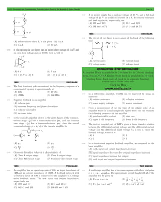
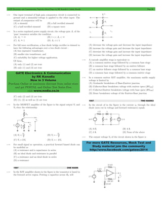


![GATE Electronics and Communication Topicwise Solved Paper by RK Kanodia & Ashish Murolia Page 88
GATE Electronics & Communication
by RK Kanodia
Now in 3 Volume
Purchase Online at maximum discount from online store
and get POSTAL and Online Test Series Free
visit www.nodia.co.in
- + - = 0
0 i 0 Vo
V
=- 2
o R
= s
= s + s s
= (1000 W) + (93 kW || 259 W) = 1258 W
1
p C L 2 = +
fo
1
= = # # # #
-
6 Lower cut-off frequency
. o 27.1Hz 10
For more GATE Resources, Mock Test and
Study material join the community
http://www.facebook.com/gateec2014
The equivalent circuit of given amplifier circuit (when CE is
connected, RE is short-circuited)
Input impedance Ri = RB || r p
Voltage gain AV = gmRC
Now, if CE is disconnected, resistance RE appears in the circuit
Input impedance Rin = RB || [rp + (b + 1)]RE
Input impedance increases
Voltage gain AV g R
g R
1 m E
= m C + Voltage gain decreases.
4.23 Option (B) is correct.
Since, emitter area of transistor Q1 is half of transistor Q2, so current
1
1
E2 B1 B2 = =
IE 2 I and I I
1 2
The circuit is as shown below :
VB =- 10 - (- 0.7) =- 9.3 V
Collector current
I1
( . )
(9.3 )
1
k
mA
0 93
= W - - =
b1 = 700 (high), So IC IE 1 .
Applying KCL at base we have
1 - IE IB1 IB 2 = +
1 ( 1 1) IB1 - b + IB1 IB 2 = +
1 (700 1 1) I2 B
I
= + + 2
+
B
2 . 2
IB 2 702
I0 IC 2 = 2 IB 2
2 = # . 2mA
= b : 715 702
4.24 Option (A) is correct.
The circuit is as shown below :
So, R
V
R
1 2
or V
i
R
1
4.25 Option (B) is correct.
By small signal equivalent circuit analysis
Input resistance seen by source vs
Rin || i v
R R r
s
4.26 Option (B) is correct.
Cut-off frequency due to C2
fo
2 (R R )C
. .
271 Hz
2 3 14 1250 4 7 10
fL f
10
= 271 =
4.27 Option (B) is correct.
The circuit is as shown below](https://image.slidesharecdn.com/kanodiamuroliapreviousyears-141121003216-conversion-gate02/85/Kanodia-murolia-previousyears-90-320.jpg)
![GATE Electronics and Communication Topicwise Solved Paper by RK Kanodia & Ashish Murolia Page 96
Vo 50 40 40 8000
1
= = # # =
1 idt t
= #
= = 1 = 2 m sec
- = 1
#
# GATE Electronics & Communication
by RK Kanodia
Now in 3 Volume
Purchase Online at maximum discount from online store
and get POSTAL and Online Test Series Free
visit www.nodia.co.in
V f
( )
V f
1 R
O
= = + 2
V f
( )
V f
1 0
= + = f
1 R
= + 2
dVO A V cos t = V mw w
dV
O c m = AVVmw = AVVm2pf
SR
V 2p
1
= -
6 # # p # #
3 or VM = 79.5 mV
Vin - V0 > I I Z + L [IZ + IL = I]
30 - 10 $ (10 + 1) mA
20 $ 11 mA
50 - 10 $ (10 + 1) mA
For more GATE Resources, Mock Test and
Study material join the community
http://www.facebook.com/gateec2014
or V3 = 40 # 40V1
Vo = 50V3 = 50 # 40 # 40V1
or AV
V
or 20 logAV = 20 log 8000 = 98 dB
4.94 Option (D) is correct.
If a constant current is made to flow in a capacitor, the output
voltage is integration of input current and that is sawtooth waveform
as below :
VC
C
0
The time period of wave form is
T
f 1
500
Thus 3 idt
2 10
6
0
20 10 3
#
or i (2 10 3 0) # - - 6 10 6 = # -
or i = 3 mA
Thus the charging require 3 mA current source for 2 msec.
4.95 Option (C) is correct.
In voltage-amplifier or voltage-series amplifier, the Ri increase and
Ro decrease because
Rif = Ri (1 + Ab)
Rof
R
1
o
b
( A )
=
+
4.96 Option (B) is correct.
Let x be the gain and it is 20 db, therefore
20 log x = 20
or x = 10
Since Gain band width product is 106 Hz, thus
So, bandwidth is
BW 10
6
Gain
=
6
10 10
= = 5 Hz = 100 kHz
10
4.97 Option (A) is correct.
In multistage amplifier bandwidth decrease and overall gain increase.
From bandwidth point of view only options (A) may be correct
because lower cutoff frequency must be increases and higher must
be decreases. From following calculation we have
We have fL = 20 Hz and fH = 1 kHz
For n stage amplifier the lower cutoff frequency is
fLn f
L
1 =
-
2n 1
20 39 2 40
3
= .
.
1
-
2 1
=
Hz
The higher cutoff frequency is
fHn . f 2 1 0 5 H 2 1
= - = kHz
4.98 Option (A) is correct.
As per Barkhousen criterion for sustained oscillations Ab $ 1 and
phase shift must be or 2pn.
Now from circuit A
( )
R
f
1
b(f)
( )
6
O
Thus from above equation for sustained oscillation
6
R
1
or R2 = 5R1
4.99 Option (C) is correct.
Let the gain of OPAMP be AV then we have
20 logAV = 40 dB
or AV = 100
Let input be Vi = Vm sinwt then we have
VO = VVVi = Vm sinwt
Now
dt
Slew Rate
dt
max
or Vm
A V f
=
10 100 2 20 10
4.100 Option (A) is correct.
The circuit is shown as below
I = IZ + IL
For satisfactory operations
R
When Vin = 30 V,
R
or
R
or R # 1818 W
when Vin = 50 V
R
40 11 10 3 $ # -
R
or R # 3636W
Thus R # 1818W
4.101 Option (D) is correct.
We have
IDSS = 10 mA and VP =- 5 V
Now VG = 0
and VS = IDRS = 1 # 2.5W = 2.5 V
Thus VGS = VG - VS = 0 - 2.5 =- 2.5 V](https://image.slidesharecdn.com/kanodiamuroliapreviousyears-141121003216-conversion-gate02/85/Kanodia-murolia-previousyears-98-320.jpg)
![GATE Electronics and Communication Topicwise Solved Paper by RK Kanodia & Ashish Murolia Page 99
= # D
V
1
2 2
SPECIAL EDITION ( STUDY MATERIAL FORM )
At market Book is available in 3 volume i.e. in 3 book binding
form. But at NODIA Online Store book is available in 10 book
binding form. Each unit of Book is in separate binding.
Available Only at NODIA Online Store
Click to Buy
www.nodia.co.in
transistor are operated one for amplifying +ve going portion and
other for -ve going portion.
4.124 Option (C) is correct.
In Voltage series feedback mode input impedance is given by
Rin = Ri (1 + bvAv)
where bv = feedback factor,
Av = openloop gain
and Ri = Input impedance
So, Rin = 1#103(1 + 0.99#100) = 100 kW
Similarly output impedance is given by
ROUT
R
= 0
+ b R0 = output impedance
(1 A )
v v
Thus ROUT
100 1
= + = W
(1 0.99 #
100)
4.125 Option (B) is correct.
= V no - load- V
fuel -
load
Regulation V
-
full load
= 30 - 25 #100 = 20
25 %
= 25 = 25 W
Output resistance 1
4.126 Option (D) is correct.
This is a voltage shunt feedback as the feedback samples a portion
of output voltage and convert it to current (shunt).
4.127 Option (A) is correct.
In a differential amplifier CMRR is given by
CMRR
(1 )
V
I R
1 1
2
T
Q 0
b
= + + b
; E
So where R0 is the emitter resistance. So CMRR can be improved
by increasing emitter resistance.
4.128 Option (C) is correct.
We know that rise time (tr ) is
tr .
0 35
f
H
=
where fH is upper 3 dB frequency. Thus we can obtain upper 3 dB
frequency it rise time is known.
4.129 Option (D) is correct.
In a BJT differential amplifier for a linear response Vid < VT .
4.130 Option (D) is correct.
In a shunt negative feedback amplifier.
Input impedance
Rin
Rib
= +
(1 A)
where Ri = input impedance of basic amplifier
b = feedback factor
A = open loop gain
So, Rin < Ri
Similarly
ROUT
R0b
= +
(1 A)
ROUT < R0
Thus input & output impedances decreases.
4.131 Option (A) is correct.
4.132 Option (D) is correct.
Comparator will give an output either equal to +Vsupply or -Vsupply.
So output is a square wave.
4.133 Option (C) is correct.
In series voltage regulator the pass transistor is in common collec-tor
configuration having voltage gain close to unity.
4.134 Option (D) is correct.
In bridge rectifier we do not need central tap transformer, so its less
expensive and smaller in size and its PIV (Peak inverse voltage)
is also greater than the two diode circuit, so it is also suitable for
higher voltage application.
4.135 Option (C) is correct.
In the circuit we have
V2 I R
S 2
and V1 = IS #RD
V
= 1
V1 = 2V2
4.136 Option (C) is correct.
4.137 Option (C) is correct.
The equivalent circuit of given amplifier circuit (when CE is
connected, RE is short-circuited)
Input impedance Ri = RB || r p
Voltage gain AV = gmRC
Now, if CE is disconnected, resistance RE appears in the circuit
Input impedance Rin = RB || [rp + (b + 1)]RE
Input impedance increases
Voltage gain AV g R
g R
1 m E
= m C + Voltage gain decreases.
4.138 Option (A) is correct.
In common emitter stage input impedance is high, so in cascaded
amplifier common emitter stage is followed by common base stage.
4.139 Option (C) is correct.
We know that collect-emitter break down voltage is less than
compare to collector base breakdown voltage.
BVCEO < BVCBO
both avalanche and zener break down. Voltage are higher than](https://image.slidesharecdn.com/kanodiamuroliapreviousyears-141121003216-conversion-gate02/85/Kanodia-murolia-previousyears-101-320.jpg)


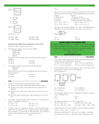


![GATE Electronics and Communication Topicwise Solved Paper by RK Kanodia & Ashish Murolia Page 119
= m b l8 ^ - h- 2 B
= m C
b l ^ - h- 2
L W
p OX
= D + 3
SPECIAL EDITION ( STUDY MATERIAL FORM )
At market Book is available in 3 volume i.e. in 3 book binding
form. But at NODIA Online Store book is available in 10 book
binding form. Each unit of Book is in separate binding.
Available Only at NODIA Online Store
Click to Buy
www.nodia.co.in
And it will remain same for the clock period. So race around
doesn’t occur for the condition.
3. Option (D): When CLK = 1, A = B = 0
So, A1 = B1 = 1
And again as described for Option (B) race around doesn’t occur
for the condition.
5.5 Option ( ) is correct.
Y = 1, when A > B
A = a1a0, B = b1b0
a1 a0 b1 b0 Y
0 1 0 0 1
1 0 0 0 1
1 0 0 1 1
1 1 0 0 1
1 1 0 1 1
1 1 1 0 1
Total combination = 6
5.6 Option (A) is correct.
Parallel connection of MOS & OR operation
Series connection of MOS & AND operation
The pull-up network acts as an inverter. From pull down network
we write Y = (A + B)C = (A + B) + C = A B + C
5.7 Option (A) is correct.
Prime implicants are the terms that we get by solving K-map
= +
1442443
F XY XY
prime implicants
5.8 Option (A) is correct.
Given the circuit as below :
Since all the parameters of PMOS and NMOS are equal.
So, mn = mp
b l C L W
C L OX
W
M1
C L W
= OX
b l = b l
M
OX
2
Given that M1 is in linear region. So, we assume that M2 is either in
cutoff or saturation.
Case 1 : M2 is in cut off
So, I2 = I1 = 0
Where I1 is drain current in M1 and I2 is drain current in M2.
Since, I1
C
L W
p 2OX 2V V V V
SD SG Tp SD
& 0 [2 ]
2 V V V V
SD SG Tp SD
Solving it we get,
2^VSG - VTph = VSD
& 2^5 - Vin - 1h = 5 - VD
& Vin V
2
For I1 = 0, VD = 5 V
So, Vin = 5 + 3 2 =
4 V
So for the NMOS
VGS = Vin - 0 = 4 - 0 = 4 V and VGS > VTn
So it can’t be in cutoff region.
Case 2 : M2 must be in saturation region.
So, I1 = I2
m C
6 ( - )
- 2 @ C ( )
L W V V V V 2 2 p OX
SG Tp SD SD
= m - 2
L W
n OX
2 V V
GS Tn
- - 2 (V V ) GS Tn
& 2(VSG VTp)VSD VSD
= - 2
- - - - - 2 (V 0 1) in
& 2(5 Vin 1) (5 VD) (5 VD)
= - - 2
- - - - 2 (V 1) in
& 2(4 Vin) (5 VD) (5 VD)
= - 2
Substituting VD = VDS = VGS - VTn and for N -MOS & VD = Vin - 1
& 2(4 - Vin) (6 - Vin) - (6 - Vin)
2 = (V in
- 1) 2
& 48 - 36 - 8Vin =- 2Vin + 1
& 6Vin = 11
& Vin = 11 6 =
1.833 V
So for M2 to be in saturation Vin < 1.833 V or Vin < 1.875 V
5.9 Option (D) is correct.
Let Qn+1 is next state and Qn is the present state. From the given
below figure.
D = Y = AX0+ AX1
Qn+1 = D = AX0+ AX1
Qn+1 = AQn + AQn X0 = Q, X1 = Q
If A = 0, Qn+1 = Qn (toggle of previous state)
If A = 1, Qn+1 = Qn
So state diagram is
5.10 Option (B) is correct.
The given circuit is shown below:](https://image.slidesharecdn.com/kanodiamuroliapreviousyears-141121003216-conversion-gate02/85/Kanodia-murolia-previousyears-122-320.jpg)
![GATE Electronics and Communication Topicwise Solved Paper by RK Kanodia & Ashish Murolia Page 121
SPECIAL EDITION ( STUDY MATERIAL FORM )
At market Book is available in 3 volume i.e. in 3 book binding
form. But at NODIA Online Store book is available in 10 book
binding form. Each unit of Book is in separate binding.
Available Only at NODIA Online Store
Click to Buy
www.nodia.co.in
For two variables A5B = A9B
So, (A5B)9(A9B) = 0 (always)
F = 09C = 0 $ C + 1 $ C = C
So, F = 1 when C = 1 or C = 0
5.19 Option (D) is correct.
Let QA(n),QB (n),QC (n) are present states and QA(n + 1),QB (n + 1),
QC (n + 1) are next states of flop-flops.
In the circuit
QA(n + 1) = QB (n)9QC (n)
QB (n + 1) QA(n)
QC (n + 1) QB (n)
Initially all flip-flops are reset
1st clock pulse
QA = 090 = 1
QB = 0
QC = 0
2nd clock pulse
QA = 090 = 1
QB = 1
QC = 0
3rd clock pulse
QA = 190 = 0
QB = 1
QC = 1
4th clock pulse
QA = 191 = 1
QB = 0
QC = 1
So, sequence QA = 01101.......
5.20 Option (D) is correct.
Output of the MUX can be written as
F = I0S0S1+ I1S0S1+ I2S0S1+ I3S0S1
Here, I0 = C, I1 = D, I2 = C, I3 = CD
and S0 = A,S1 = B
So, F = C A B + D A B + CAB + C DAB
Writing all SOP terms
= + + +
1442443 1442443 S 1442443
F A B C D A B C D A BCD A BC D
m3 m2 m7 m5
+ ABC D + ABC D +
1442443 1442443 ABC S
D
m9 m8 m12
F = /m(2,3,5,7,8,9,12)
5.21 Option (C) is correct.
By executing instruction one by one
MVI A, 45 H & MOV 45 H into accumulator, A = 45 H
STC & Set carry, C = 1
CMC & Complement carry flag, C = 0
RAR & Rotate accumulator right through carry
A = 00100010
XRA B & XOR A and B
A = A5B = 00100010501000101 = 01100111 = 674
5.22 Option (C) is correct.
TTL " Transistor - Transistor logic
CMOS " Complementary Metal Oxide Semi-conductor
5.23 Option (D) is correct.
Vectored interrupts : Vectored interrupts are those interrupts in
which program control transferred to a fixed memory location.
Maskable interrupts : Maskable interrupts are those interrupts which
can be rejected or delayed by microprocessor if it is performing some
critical task.
5.24 Option (D) is correct.
We have 6X + Z{Y + (Z + XY)}@[X + Z(X + Y)] = 1
Substituting X = 1 and X = 0 we get
[1 + Z{Y + (Z + 1Y)}][0 + Z(1 + Y)] = 1
or [1][Z(1)] = 1 1 + A = 1 and 0 + A = A
or Z = 1 ) Z = 0
5.25 Option (A) is correct.
The AND gate implementation by 2:1 mux is as follows
Y = AI0+ AI1 = AB
The EX - OR gate implementation by 2:1 mux is as follows
Y = BI0+ BI1 = AB + BA
5.26 Option (A) is correct.
The given circuit is as follows.
The truth table is as shown below. Sequence is 00, 11, 10, 00 ...
CLK J1 K1 Q1 J2 K2 Q2
1 1 1 0 1 1 0
2 1 1 1 1 1 1
3 0 0 1 0 1 0
4 1 1 0 1 1 0](https://image.slidesharecdn.com/kanodiamuroliapreviousyears-141121003216-conversion-gate02/85/Kanodia-murolia-previousyears-124-320.jpg)

![GATE Electronics and Communication Topicwise Solved Paper by RK Kanodia & Ashish Murolia Page 124
GATE Electronics & Communication
by RK Kanodia
Now in 3 Volume
Purchase Online at maximum discount from online store
and get POSTAL and Online Test Series Free
visit www.nodia.co.in
For more GATE Resources, Mock Test and
Study material join the community
http://www.facebook.com/gateec2014
be 0 or.
1. Thus address range is
1 1 1 1 1 0 0 0 F8H
1 1 1 1 1 1 1 1 FFH
5.46 Option (B) is correct.
Since the inverting terminal is at virtual ground the resistor network
can be reduced as follows
The current from voltage source is
I
V
= R = 10 = 1 mA
R
10k
This current will be divide as shown below
3 = = # =
Now i I .
1 10 62 5
16 16
-
m A
5.47 Option (C) is correct.
The net current in inverting terminal of OP - amp is
I- = 1
+ = 5
I
4
1
16
16
So that V0 R I .
=- # 5 =- 3 125
16
5.48 Option (B) is correct.
Line
1 : MVI A, B5H ; Move B5H to A
2 : MVI B, 0EH ; Move 0EH to B
3 : XRI 69H ; [A] XOR 69H and store in A
; Contents of A is CDH
4 : ADDB ; Add the contents of A to contents of B and
; store in A, contents of A is EAH
5 : ANI 9BH ; [a] AND 9BH, and store in A,
; Contents of A is 8 AH
6 : CPI 9FH ; Compare 9FH with the contents of A
; Since 8 AH < 9BH, CY = 1
7 : STA 3010 H ; Store the contents of A to location 3010
H
8 : HLT ; Stop
Thus the contents of accumulator after execution of ADD instruction
is EAH.
5.49 Option (C) is correct.
The CY = 1 and Z = 0
5.50 Option (A) is correct.
For this circuit the counter state (Q1,Q0) follows the sequence 00, 01,
10, 00 ... as shown below
Clock D1D0 Q1Q0 Q1 NOR Q0
00 1
1st 01 10 0
2nd 10 01 0
3rd 00 00 0
5.51 Option (A) is correct.
As shown below there are 2 terms in the minimized sum of product
expression.
1 0 0 1
0 d 0 0
0 0 d 1
1 0 0 1
5.52 Option (B) is correct.
The output is taken from the 5th line.
5.53 Option (D) is correct.
After applying two clock poles, the outputs of the full adder is S = 1
, C0 = 1
A B Ci S Co
1st 1 0 0 0 1
2nd 1 1 1 1 1
5.54 Option (D) is correct.
100010011001
4 2 3 1
SSSS
5.55 Option (B) is correct.
In this the diode D2 is connected to the ground. The following table
shows the state of counter and D/A converter
Q2Q1Q0 D3 = Q2 D2 = 0 D1 = Q1 D0 = Q0 Vo
000 0 0 0 0 0
001 0 0 0 1 1
010 0 0 1 0 2
011 0 0 1 1 3](https://image.slidesharecdn.com/kanodiamuroliapreviousyears-141121003216-conversion-gate02/85/Kanodia-murolia-previousyears-127-320.jpg)
![GATE Electronics and Communication Topicwise Solved Paper by RK Kanodia & Ashish Murolia Page 125
SPECIAL EDITION ( STUDY MATERIAL FORM )
At market Book is available in 3 volume i.e. in 3 book binding
form. But at NODIA Online Store book is available in 10 book
binding form. Each unit of Book is in separate binding.
Available Only at NODIA Online Store
Click to Buy
www.nodia.co.in
100 1 0 0 0 8
101 1 0 0 1 9
110 1 0 1 0 10
111 1 0 1 1 11
000 0 0 0 0 0
001 0 0 0 1 1
Thus option (B) is correct
5.56 Option (B) is correct.
LXI, EFFF H ; Load SP with data EFFH
CALL 3000 H ; Jump to location 3000 H
:
:
:
3000H LXI H, 3CF4 ; Load HL with data 3CF4H
PUSH PSW ; Store contnets of PSW to Stack
POP PSW ; Restore contents of PSW from stack
PRE ; stop
Before instruction SPHL the contents of SP is 3CF4H.
After execution of POP PSW, SP + 2 " SP
After execution of RET, SP + 2 " SP
Thus the contents of SP will be 3CF4H + 4 = 3CF8H
5.57 Option (A) is correct.
The inputs D0 and D1 respectively should be connected as Q1 and Q0
where Q0 " D1 and Q1 " D0
5.58 Option (D) is correct.
If the point P is stuck at 1, then output f is equal to A
5.59 Option (B) is correct.
Dividing 43 by 16 we get
2 g
16 43
32
11
11 in decimal is equivalent is B in hexamal.
Thus 4310*2B16
Now 410*01002
310*00112
Thus 4310*01000011BCD
5.60 Option (A) is correct.
The diagram is as shown in fig
f' = BC + BC
f = f'A + f'0 = f'A = ABC + ABC
5.61 Option (C) is correct.
The circuit is as shown below
If output is at logic 0, the we have V0 = 0 which signifies BJT Q3 is
in saturation and applying KVL we have
VBE3 = IR # 1k
or 0.75 = IR # 1k
or IR = 0.75 mA
5.62 Option (A) is correct.
We have f = ABC + ABC
= B(AC + AC) = B(A + C)(A + C)
5.63 Option (C) is correct.
Characteristic equation for a jk flip-flop is written as
Qn+1 = JQn + KQn
Where Qn is the present output
Qn+1 is next output
So, Qn+1 = 10 + K : 0 Qn = 0
Qn+1 = 1
5.64 Option (C) is correct.
Since T2T1T0 is at 111, at every clock Q2Q1Q0 will be changes. Ir
present state is 011, the next state will be 100.
5.65 Option (D) is correct.
5.66 Option (C) is correct.
0100H LXI SP, 00FF ; Load SP with 00FFG
0103H LXI H, 0701 ; Load HL with 0107H
0106H MVI A, 20H ; Move A with 20 H
0108 H SUB M ; Subtract the contents of memory
; location whose address is stored in HL
; from the A and store in A
0109H ORI 40H ; 40H OR [A] and store in A
010BH ADD M ; Add the contents of memeory location
; whose address is stored in HL to A
; and store in A
HL contains 0107H and contents of 0107H is 20H
Thus after execution of SUB the data of A is 20H - 20H = 00
5.67 Option (C) is correct.
Before ORI instruction the contents of A is 00H. On execution the
ORI 40H the contents of A will be 40H
00H = 00000000
40H = 01000000
ORI 01000000](https://image.slidesharecdn.com/kanodiamuroliapreviousyears-141121003216-conversion-gate02/85/Kanodia-murolia-previousyears-128-320.jpg)

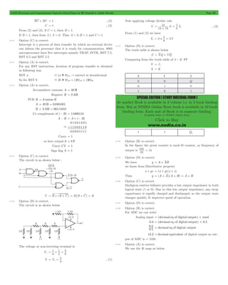
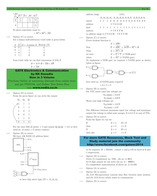
![GATE Electronics and Communication Topicwise Solved Paper by RK Kanodia & Ashish Murolia Page 131
SPECIAL EDITION ( STUDY MATERIAL FORM )
At market Book is available in 3 volume i.e. in 3 book binding
form. But at NODIA Online Store book is available in 10 book
binding form. Each unit of Book is in separate binding.
Available Only at NODIA Online Store
Click to Buy
www.nodia.co.in
5.134 Option (B) is correct.
Dual slope ADC is more accurate.
5.135 Option (A) is correct.
Dual form of any identity can be find by replacing all AND function
to OR and vice-versa. so here dual form will be
(A + B) (A + C) (B + C) = (A + B) (A + C)
5.136 Option (B) is correct.
Carry flag will be affected by arithmetic instructions only.
5.137 Option (C) is correct.
This is a synchronous counter. we can find output as
Q Q
0
1
0
0
A B
0
0
1
0
h
So It counts only three states. It is a mod-3 counter.
K = 3
5.138 Option (B) is correct.
5.139 Option (A) is correct.
Essential prime implicates for a function is no. of terms that we get
by solving K-map. Here we get 4 terms when solve the K-map.
y = B D + AC D + C AB + CA B
so no of prime implicates is 4
5.140 Option (A) is correct.
5.141 Option (B) is correct.
For a 2 bit multiplier
B 1 B
0
A 1 A
0
A B A B
0 1 0 0
#
A B A B
1 1 1 0
#
C C C C
3 2 1 0
This multiplication is identical to AND operation and then addition.
5.142 Option (C) is correct.
In totem pole stage output resistance will be small so it acts like a
output buffer.
5.143 Option (B) is correct.
Consider high output state
I 400
20
IH
max
= OH = =
fan out max
20
mA
mA
I
Consider low output state
I 8
80
IL
max
mA
= OL = =
fan out max
0.1
mA
I
Thus fan out is 20
5.144 Option (A) is correct.
The given gate is ex-OR so output
F = AB + AB
Here input B = 0 so,
F = A1 + A0 = A
5.145 Option (C) is correct.
EI =Enabled Interput flag,RST will cause an Interrupt
only it we enable EI .
5.146 Option (A) is correct.
Here only for the range 60 to 63 H chipselect will be 0, so peripheral
will correspond in this range only chipselect = 1 for rest of the given
address ranges.
5.147 Option (B) is correct.
By executing instructions one by one
LXI H, 8A79 H (Load HL pair by value 8A79)
H = 8AH L = 79 H
MOV A,L (copy contain of L to accumulator)
A = 79 H
ADDH (add contain of H to accumulator)
A = 79 H = 0 1111 0 0 1
H = 8AH = add 1 0 0 0 1 0 1 0
= A = 0 0 0 0 0 0 11
Carry = 1
DAA (Carry Flag is set, so DAA adds 6 to high order four bits)
01111 0 01
DAA add 1 0 0 01 01 0
A = 0 0 0 0 0 0 11 = 63 H
MOV H, A (copy contain of A to H)
H = 63 H
PCHL (Load program counter by HL pair)
PC = 6379 H
5.148 Option (C) is correct.
5.149 Option (C) is correct.
NMOS In parallel makes OR Gate & in series makes AND so here
we can have
F = A(B + C) + DE
we took complement because there is another NMOS given above
(works as an inverter)
5.150 Option (D) is correct.
For a J -K flip flop we have characteristic equation as
Q(t + 1) = JQ(t) + KQ(t)
Q(t)&Q(t + 1) are present & next states.
In given figure J = Q(t), K = 1 so
Q(t + 1) = Q(t)Q(t) + 0Q(t)
Q(t + 1) = Q(t)[complement of previous state]
we have initial input Q(t) = 0](https://image.slidesharecdn.com/kanodiamuroliapreviousyears-141121003216-conversion-gate02/85/Kanodia-murolia-previousyears-134-320.jpg)
![GATE Electronics and Communication Topicwise Solved Paper by RK Kanodia & Ashish Murolia Page 134
< < 1
1 < < 3 (D) z 3
t
-3 # . The system is
= t t t
GATE Electronics & Communication
by RK Kanodia
Now in 3 Volume
Purchase Online at maximum discount from online store
and get POSTAL and Online Test Series Free
visit www.nodia.co.in
-
1
-
1 06
.
1 1
z
- -
-
z 1 04
z
- -
1 -
1
-
z z
1 04
( 1 06
. )
-
z
1
- -
1 -
1
-
z z
1 06
( 1 04
. )
-
z
1
-
1
-
1 04
.
1 1
z
- -
-
z 1 06
z
For more GATE Resources, Mock Test and
Study material join the community
http://www.facebook.com/gateec2014
6.13 If x[n] = (1/3) n - (1/2)nu[n], then the region of convergence (ROC)
of its z -transform in the z -plane will be
(A) 3 z
1 < < 3 (B) 1
3
z 2
(C) 2 z
1 <
2012 TWO MARKS
6.14 The input x(t) and output y(t) of a system are related as
y(t) x( )cos (3 )d
(A) time-invariant and stable (B) stable and not time-invari-ant
(C) time-invariant and not stable (D) not time-invariant and not
stable
6.15 The Fourier transform of a signal h(t) is H(jw) = (2 cosw) (sin2w)/w
. The value of h(0) is
(A) 1/4 (B) 1/2
(C) 1 (D) 2
6.16 Let y[n] denote the convolution of h[n] and g[n], where
h[n] = (1/2)nu[n] and g[n] is a causal sequence. If y[0] = 1 and
y[1] = 1/2, then g[1] equals
(A) 0 (B) 1/2
(C) 1 (D) 3/2
2011 ONE MARK
2 - + = describes a system
d y
dy
6.17 The differential equation 100 20 y x(t) dt
2
dt
with an input x(t) and an output y(t). The system, which is initially
relaxed, is excited by a unit step input. The output y^t h can be
represented by the waveform
6.18 The trigonometric Fourier series of an even function does not have
the
(A) dc term (B) cosine terms
(C) sine terms (D) odd harmonic terms
6.19 A system is defined by its impulse response h(n) = 2nu(n - 2). The
system is
(A) stable and causal (B) causal but not stable
(C) stable but not causal (D) unstable and non-causal
6.20 If the unit step response of a network is (1 - e-at), then its unit
impulse response is
(A) ae-at (B) a-1e-at
(C) (1 - a-1)e-at (D) (1 - a)e-at
2011 TWO MARKS
6.21 An input x(t) = exp(- 2t)u(t) + d(t - 6) is applied to an LTI system
with impulse response h(t) = u(t) . The output is
(A) [1 - exp(- 2t)]u(t) + u(t + 6)
(B) [1 - exp(- 2t)]u(t) + u(t - 6)
(C) 0.5[1 - exp(- 2t)]u(t) + u(t + 6)
(D) 0.5[1 - exp(- 2t)]u(t) + u(t - 6)
6.22 Two systems H1(Z) and H2(Z) are connected in cascade as shown
below. The overall output y(n) is the same as the input x(n) with a
one unit delay. The transfer function of the second system H2(Z) is
(A)
( . )
(B)
( . )
(C)
( . )
(D)
( . )
6.23 The first six points of the 8-point DFT of a real valued sequence are
5, 1 - j3, 0, 3 - j 4, 0 and 3 + j 4. The last two points of the DFT
are respectively
(A) 0, 1 - j3 (B) 0, 1 + j3
(C) 1 + j3, 5 (D) 1 - j3, 5
2010 ONE MARK
6.24 The trigonometric Fourier series for the waveform f (t) shown below
contains
(A) only cosine terms and zero values for the dc components](https://image.slidesharecdn.com/kanodiamuroliapreviousyears-141121003216-conversion-gate02/85/Kanodia-murolia-previousyears-137-320.jpg)
![GATE Electronics and Communication Topicwise Solved Paper by RK Kanodia & Ashish Murolia Page 135
1
p Hz
1
p and 1p
0 1
p and 1p
1
n 1 n
= b l -b l - - is
< < 1 (B) z
> 1
SPECIAL EDITION ( STUDY MATERIAL FORM )
1
At market Book is available in 3 volume i.e. in 3 book binding
form. But at NODIA Online Store book is available in 10 book
binding form. Each unit of Book is in separate binding.
Available Only at NODIA Online Store
Click to Buy
www.nodia.co.in
(B) only cosine terms and a positive value for the dc components
(C) only cosine terms and a negative value for the dc components
(D) only sine terms and a negative value for the dc components
6.25 Consider the z -transform x(z) = 5z2+ 4z-1+ 3; 0 < z < 3. The
inverse z - transform x[n] is
(A) 5d[n + 2] + 3d[n] + 4d[n - 1]
(B) 5d[n - 2] + 3d[n] + 4d[n + 1]
(C) 5u[n + 2] + 3u[n] + 4u[n - 1]
(D) 5u[n - 2] + 3u[n] + 4u[n + 1]
6.26 Two discrete time system with impulse response h1[n] = d[n - 1]
and h2[n] = d[n - 2] are connected in cascade. The overall impulse
response of the cascaded system is
(A) d[n - 1] + d[n - 2] (B) d[n - 4]
(C) d[n - 3] (D) d[n - 1]d[n - 2]
6.27 For a N -point FET algorithm N = 2m which one of the following
statements is TRUE ?
(A) It is not possible to construct a signal flow graph with both
input and output in normal order
(B) The number of butterflies in the mth stage in N/m
(C) In-place computation requires storage of only 2N data
(D) Computation of a butterfly requires only one complex multipli-cation.
2010 TWO MARKS
6.28 Given ( )
- 1 3 + 1
; E. If limf (t) 1
+ + -
( )
3 2 =
f t L
s
s 4 s k 3
s
t
=
"3
, then the value
of k is
(A) 1 (B) 2
(C) 3 (D) 4
6.29 A continuous time LTI system is described by
d y t
( )
4
y t 2
dy t
( )
3 ( )
dt
dt
2
+ +
dx t
( )
dt ( )
= 2 + 4x t
Assuming zero initial conditions, the response y(t) of the above
system for the input x(t) = e-2tu(t) is given by
(A) (et - e3t)u(t) (B) (e-t - e-3t)u(t)
(C) (e-t + e-3t)u(t) (D) (et + e3t)u(t)
6.30 The transfer function of a discrete time LTI system is given by
H(z)
-
-
z
- -
1
z z
1 4 3
8
2 4 3
1
1 2
=
- +
Consider the following statements:
S1: The system is stable and causal for ROC: z > 1/2
S2: The system is stable but not causal for ROC: z < 1/4
S3: The system is neither stable nor causal for ROC:
1/4 < z < 1/2
Which one of the following statements is valid ?
(A) Both S1 and S2 are true (B) Both S2 and S3 are true
(C) Both S1 and S3 are true (D) S1, S2 and S3 are all true
2009 ONE MARK
6.31 The Fourier series of a real periodic function has only
(P) cosine terms if it is even
(Q) sine terms if it is even
(R) cosine terms if it is odd
(S) sine terms if it is odd
Which of the above statements are correct ?
(A) P and S (B) P and R
(C) Q and S (D) Q and R
6.32 A function is given by f (t) = sin2t + cos 2t . Which of the following
is true ?
(A) f has frequency components at 0 and
2
(B) f has frequency components at 0 and 1p
Hz
(C) f has frequency components at
2
Hz
(D) f has frequency components at .
2
Hz
6.33 The ROC of z -transform of the discrete time sequence
x(n) 3 u(n) 2
u( n 1)
(A) z
3
2
2
(C) z
< 1 (D) 2 < z < 3
3
2009 TWO MARKS
6.34 Given that F(s) is the one-side Laplace transform of f (t), the Laplace
t
# t t is
transform of f ( )d
0
1 F s
(A) sF(s) - f (0) (B) ( )
s
# t t (D) [ ( ) ( )]
s
0
(C) F( )d
1 F s - f 0
s
6.35 A system with transfer function H(z) has impulse response h(.)
defined as h(2) = 1,h(3) =- 1 and h(k) = 0 otherwise. Consider the
following statements.
S1 : H(z) is a low-pass filter.
S2 : H(z) is an FIR filter.
Which of the following is correct?
(A) Only S2 is true
(B) Both S1 and S2 are false
(C) Both S1 and S2 are true, and S2 is a reason for S1
(D) Both S1 and S2 are true, but S2 is not a reason for S1
6.36 Consider a system whose input x and output y are related by the
3
-# where h(t) is shown in the graph.
equation y(t) = x(t - t)g(2t)dt
3
Which of the following four properties are possessed by the system
?
BIBO : Bounded input gives a bounded output.](https://image.slidesharecdn.com/kanodiamuroliapreviousyears-141121003216-conversion-gate02/85/Kanodia-murolia-previousyears-138-320.jpg)
![GATE Electronics and Communication Topicwise Solved Paper by RK Kanodia & Ashish Murolia Page 136
+ 1
and input
s
GATE Electronics & Communication
by RK Kanodia
Now in 3 Volume
Purchase Online at maximum discount from online store
and get POSTAL and Online Test Series Free
visit www.nodia.co.in
-/
N
1
= +
-/
N
1
-/
N
1
For more GATE Resources, Mock Test and
Study material join the community
http://www.facebook.com/gateec2014
Causal : The system is causal,
LP : The system is low pass.
LTI : The system is linear and time-invariant.
(A) Causal, LP (B) BIBO, LTI
(C) BIBO, Causal, LTI (D) LP, LTI
6.37 The 4-point Discrete Fourier Transform (DFT) of a discrete time
sequence {1,0,2,3} is
(A) [0, -2 + 2j , 2, -2 - 2j ] (B) [2, 2 + 2j , 6, 2 - 2j ]
(C) [6, 1 - 3j , 2, 1 + 3j ] (D) [6, -1 + 3j , 0, -1 - 3j ]
6.38 An LTI system having transfer function s 2
2 s
1
2
+ +
x(t) = sin(t + 1) is in steady state. The output is sampled at a rate
ws rad/s to obtain the final output {x(k)}. Which of the following
is true ?
(A) y(.) is zero for all sampling frequencies ws
(B) y(.) is nonzero for all sampling frequencies ws
(C) y(.) is nonzero for ws > 2 , but zero for ws < 2
(D) y(.) is zero for ws > 2, but nonzero for w2 < 2
2008 ONE MARK
6.39 The input and output of a continuous time system are respectively
denoted by x(t) and y(t). Which of the following descriptions
corresponds to a causal system ?
(A) y(t) = x(t - 2) + x(t + 4) (B) y(t) = (t - 4)x(t + 1)
(C) y(t) = (t + 4)x(t - 1) (D) y(t) = (t + 5)x(t + 5)
6.40 The impulse response h(t) of a linear time invariant continuous
time system is described by h(t) = exp(at)u(t) + exp(bt)u(- t)
where u(- t) denotes the unit step function, and a and b are real
constants. This system is stable if
(A) a is positive and b is positive
(B) a is negative and b is negative
(C) a is negative and b is negative
(D) a is negative and b is positive
2008 TWO MARKS
6.41 A linear, time - invariant, causal continuous time system has a
rational transfer function with simple poles at s =- 2 and s =- 4
and one simple zero at s =- 1. A unit step u(t) is applied at the
input of the system. At steady state, the output has constant value
of 1. The impulse response of this system is
(A) [exp(- 2t) + exp(- 4t)]u(t)
(B) [- 4 exp(- 2t) - 12 exp(- 4t) - exp(- t)]u(t)
(C) [- 4 exp(- 2t) + 12 exp(- 4t)]u(t)
(D) [- 0.5 exp(- 2t) + 1.5 exp(- 4t)]u(t)
6.42 The signal x(t) is described by
x(t)
1 for
1 # t #
1
0
otherwise
=
- +
)
Two of the angular frequencies at which its Fourier transform be-comes
zero are
(A) p, 2p (B) 0.5p, 1.5p
(C) 0, p (D) 2p, 2.5p
6.43 A discrete time linear shift - invariant system has an impulse
response h[n] with h[0] = 1,h[1] =- 1,h[2] = 2, and zero otherwise
The system is given an input sequence x[n] with x[0] = x[2] = 1,
and zero otherwise. The number of nonzero samples in the output
sequence y[n], and the value of y[2] are respectively
(A) 5, 2 (B) 6, 2
(C) 6, 1 (D) 5, 3
6.44 Let x(t) be the input and y(t) be the output of a continuous time
system. Match the system properties P1, P2 and P3 with system
relations R1, R2, R3, R4
Properties Relations
P1 : Linear but NOT time - invariant R1 : y(t) = t2x(t)
P2 : Time - invariant but NOT linear R2 : y(t) = t x(t)
P3 : Linear and time - invariant R3 : y(t) = x(t)
R4 : y(t) = x(t - 5)
(A) (P1, R1), (P2, R3), (P3, R4)
(B) (P1, R2), (P2, R3), (P3, R4)
(C) (P1, R3), (P2, R1), (P3, R2)
(D) (P1, R1), (P2, R2), (P3, R3)
6.45 {x(n)} is a real - valued periodic sequence with a period N . x(n)
and X(k) form N-point Discrete Fourier Transform (DFT) pairs.
The DFT Y(k) of the sequence y(n) N1 x(r)x(n r)
r
0
=
is
(A) X(k) 2 (B) N1 X(r)X(k r)
r
0
+
=
(C) N1 X(r)X(k r)
r
0
+
=
(D) 0
Statement for Linked Answer Question 6.31 and 6.32:
In the following network, the switch is closed at t = 0- and the
sampling starts from t = 0. The sampling frequency is 10 Hz.
6.46 The samples x(n), n = (0, 1, 2, ...) are given by
(A) 5(1 - e-0.05n) (B) 5e-0.05n
(C) 5(1 - e-5n) (D) 5e-5n
6.47 The expression and the region of convergence of the z -transform of
the sampled signal are
(A) ,
5z
- 5
z e
5z
- -0.05 z < e-0.05
z < e-5 (B) ,
z e
5z
- -0.05 z > e-0.05 (D)
(C) ,
z e
5z
- -5 , z > e-5
z e
Statement for Linked Answer Question 6.33 & 6.34:
The impulse response h(t) of linear time - invariant continuous](https://image.slidesharecdn.com/kanodiamuroliapreviousyears-141121003216-conversion-gate02/85/Kanodia-murolia-previousyears-139-320.jpg)
![GATE Electronics and Communication Topicwise Solved Paper by RK Kanodia & Ashish Murolia Page 137
3 d =
=
3
-#
3 d =
=
3
-#
) and d(t)dt = 1
1
< < 2 then the
1 < < 3 (B) z
2 < < 3
3 < < 3 (D) 1
z
< < 2
SPECIAL EDITION ( STUDY MATERIAL FORM )
At market Book is available in 3 volume i.e. in 3 book binding
form. But at NODIA Online Store book is available in 10 book
binding form. Each unit of Book is in separate binding.
Available Only at NODIA Online Store
Click to Buy
www.nodia.co.in
time system is given by h(t) = exp(- 2t)u(t), where u(t) denotes
the unit step function.
6.48 The frequency response H(w) of this system in terms of angular
frequency w, is given by H(w)
(A)
1
+ w (B) sin
1 j2
w
w
(C)
1
+ w (D)
2 j
w
+
j
2 j
w
6.49 The output of this system, to the sinusoidal input x(t) = 2 cos 2t for
all time t , is
(A) 0 (B) 2-0.25cos (2t - 0.125p)
(C) 2-0.5cos (2t - 0.125p) (D) 2-0.5cos (2t - 0.25p)
2007 ONE MARK
6.50 If the Laplace transform of a signal ( )
= 1
- , then its final
( )
Y s
s s 1
value is
(A) -1 (B) 0
(C) 1 (D) Unbounded
2007 TWO MARKS
6.51 The 3-dB bandwidth of the low-pass signal e-tu(t), where u(t) is the
unit step function, is given by
(A)
1
p Hz (B)
2
1 2 1 p
2
- Hz
(C) 3 (D) 1 Hz
6.52 A 5-point sequence x[n] is given as x[- 3] = 1, x[- 2] = 1, x[- 1] = 0,
x[0] = 5 and x[1] = 1. Let X(eiw) denoted the discrete-time Fourier
transform of x[n]. The value of X(ejw)dw
p
-# is
p
(A) 5 (B) 10p
(C) 16p (D) 5 + j10p
1 = - - .
6.53 The z -transform X(z) of a sequence x[n] is given by X[z] .
0 5
1 2z
It is given that the region of convergence of X(z) includes the unit
circle. The value of x[0] is
(A) -0.5 (B) 0
(C) 0.25 (D) 05
6.54 A Hilbert transformer is a
(A) non-linear system (B) non-causal system
(C) time-varying system (D) low-pass system
6.55 The frequency response of a linear, time-invariant system is given by
= 5 + p . The step response of the system is
H(f) 1 j10 f
t5
6 - - @
(A) 5(1 - e-5t)u(t) (B) 5 1 e u(t)
1 - -5t (D) e u(t) 5
(C) 2 (1 e )u(t)
1 1
t5
^ - - h
2006 ONE MARK
6.56 Let x(t)*X(jw) be Fourier Transform pair. The Fourier Transform
of the signal x(5t - 3) in terms of X(jw) is given as
(A) 1
e X j
5
- 3w w b l (B) e X j
5
j
5
1
5
3w w
5
j
5
b l
-j3w w b l (D) e X j
(C) 1
e X j
5
5
1
5
j3w w b l
5
6.57 The Dirac delta function d(t) is defined as
(A) ( ) t
1 t 0
0 otherwise
d =
=
)
(B) ( ) t
t 0
0 otherwise
)
(C) ( ) t
1 t 0
0 otherwise
d =
=
) and d(t)dt = 1
3
(D) ( ) t
t 0
0 otherwise
3
6.58 If the region of convergence of x1[n] + x2[n] is z
3
3
region of convergence of x1[n] - x2[n] includes
(A) z
3
3
(C) z
2
3
3
6.59 In the system shown below, x(t) = (sint)u(t) In steady-state, the
response y(t) will be
1
(A) sin t
2
4 p ` - j (B) sin t
1
2
4 p
` + j
1 -t (D) sint - cos t
(C) e sint
2
2006 TWO MARKS
6.60 Consider the function f (t) having Laplace transform
0
w
F(s) Re[ ]
s
s > 0 2
2
0
= w
+
The final value of f (t) would be
(A) 0 (B) 1
(C) -1 # f (3) # 1 (D) 3
= p
6.61 A system with input x[n] and output y[n] is given as y[n] (sin n)x[n] 6 5
. The system is
(A) linear, stable and invertible
(B) non-linear, stable and non-invertible
(C) linear, stable and non-invertible
(D) linear, unstable and invertible
6.62 The unit step response of a system starting from rest is given by
c(t) = 1 - e-2t for t $ 0. The transfer function of the system is
(A)
1
+ (B)
1 2s
2+
2 s
(C)
1+
2 s
(D)
s
s
2+
1 2
6.63 The unit impulse response of a system is f (t) = e-t, t $ 0. For this
system the steady-state value of the output for unit step input is
equal to
(A) -1 (B) 0
(C) 1 (D) 3](https://image.slidesharecdn.com/kanodiamuroliapreviousyears-141121003216-conversion-gate02/85/Kanodia-murolia-previousyears-140-320.jpg)
![GATE Electronics and Communication Topicwise Solved Paper by RK Kanodia & Ashish Murolia Page 139
SPECIAL EDITION ( STUDY MATERIAL FORM )
At market Book is available in 3 volume i.e. in 3 book binding
form. But at NODIA Online Store book is available in 10 book
binding form. Each unit of Book is in separate binding.
Available Only at NODIA Online Store
Click to Buy
6.74 The Fourier transform of y(2n) will be www.nodia.co.in
(A) e-j2w [cos 4w + 2 cos 2w + 2] (B) cos 2w + 2 cosw + 2
(C) e-jw [cos 2w + 2 cosw + 2] (D) e-j2w [cos 2w + 2 cos + 2]
6.75 For a signal x(t) the Fourier transform is X(f). Then the inverse
Fourier transform of X(3f + 2) is given by
(A) 1
x t e
2
4p - ` j
j3pt ` j (B) x t e
2
1
3
3
j t
3
(C) 3x(3t)e-j4pt (D) x(3t + 2)
2004 ONE MARK
6.76 The impulse response h[n] of a linear time-invariant system is given
by h[n] = u[n + 3] + u[n - 2) - 2n[n - 7] where u[n] is the unit step
sequence. The above system is
(A) stable but not causal (B) stable and causal
(C) causal but unstable (D) unstable and not causal
z
0 2 = - . If the ROC is z < 0.2
6.77 The z -transform of a system is H(z) z .
, then the impulse response of the system is
(A) (0.2)nu[n] (B) (0.2)nu[- n - 1]
(C) -(0.2)nu[n] (D) -(0.2)nu[- n - 1]
6.78 The Fourier transform of a conjugate symmetric function is always
(A) imaginary (B) conjugate anti-symmetric
(C) real (D) conjugate symmetric
2004 TWO MARKS
6.79 Consider the sequence x[n] = [- 4 - j51 + j25]
-
. The conjugate anti-symmetric
part of the sequence is
(A) [- 4 - j2.5, j2, 4 - j2.5] (B) [- j2.5, 1, j2.5]
(C) [- j2.5, j2, 0] (D) [- 4, 1, 4]
6.80 A causal LTI system is described by the difference equation
2y[n] = ay[n - 2] - 2x[n] + bx[n - 1]
The system is stable only if
(A) a = 2, b < 2 (B) a > 2, b > 2
(C) a < 2, any value of b (D) b < 2, any value of a
6.81 The impulse response h[n] of a linear time invariant system is given
as
h[n]
,
,
n
n
2 2 1 1
4 2 2 2
0 otherwise
=
- = -
* = -
If the input to the above system is the sequence ejpn/4, then the
output is
(A) 4 2 ejpn/4 (B) 4 2 e-jpn/4
(C) 4ejpn/4 (D) -4ejpn/4
6.82 Let x(t) and y(t) with Fourier transforms F(f) and Y(f) respectively
be related as shown in Fig. Then Y(f) is
-1 -jpf (B) X(f/ )e
(A) 2X(f/2)e
-1 2 j2pf
2
(C) -X(f/2)ej2pf (D) -X(f/2)e-j2pf
2003 ONE MARK
6.83 The Laplace transform of i (t) is given by
I (s)
= 2
+
s(1 s)
At t " 3, The value of i (t) tends to
(A) 0 (B) 1
(C) 2 (D) 3
6.84 The Fourier series expansion of a real periodic signal with
j2 f t = 0
fundamental frequency f0 is given by gp (t) c e
n
n
3
p
=- /
. It is given
that c3 = 3 + j5. Then c-3 is
(A) 5 + j3 (B) -3 - j5
(C) -5 + j3 (D) 3 - j5
6.85 Let x(t) be the input to a linear, time-invariant system. The required
output is 4p(t - 2). The transfer function of the system should be
(A) 4ej4pf (B) 2e-j8pf
(C) 4e-j4pf (D) 2ej8pf
6.86 A sequence x(n) with the z -transform X(z) = z4+ z2- 2z + 2 - 3z-4
is applied as an input to a linear, time-invariant system with the
impulse response h(n) = 2d(n - 3) where](https://image.slidesharecdn.com/kanodiamuroliapreviousyears-141121003216-conversion-gate02/85/Kanodia-murolia-previousyears-142-320.jpg)
![GATE Electronics and Communication Topicwise Solved Paper by RK Kanodia & Ashish Murolia Page 140
1 n 0
0 otherwise
x n n
$
= =
+ -
GATE Electronics & Communication
by RK Kanodia
Now in 3 Volume
Purchase Online at maximum discount from online store
and get POSTAL and Online Test Series Free
visit www.nodia.co.in
5
2 = - -
- and the system is stable
- and the system is unstable
1
2 =
-
# 3
b l is
For more GATE Resources, Mock Test and
Study material join the community
http://www.facebook.com/gateec2014
d(n)
,
,
=
=
)
The output at n = 4 is
(A) -6 (B) zero
(C) 2 (D) -4
2003 TWO MARKS
6.87 Let P be linearity, Q be time-invariance, R be causality and S be
stability. A discrete time system has the input-output relationship,
y(n)
( ) 1
0, n
0
( )
x n 1 n #
1
*
where x(n) is the input and y(n) is the output. The above system
has the properties
(A) P, S but not Q, R
(B) P, Q, S but not R
(C) P, Q, R, S
(D) Q, R, S but not P
Common Data For Q. 6.73 & 6.74 :
The system under consideration is an RC low-pass filter (RC-LPF)
with R = 1 kW and C = 1.0 mF.
6.88 Let H(f) denote the frequency response of the RC-LPF. Let f1 be
the highest frequency such that
H f
( )
1
# f # f 1 $ 0 .
95
. Then f1
( )
H
0
0
(in Hz) is
(A) 324.8 (B) 163.9
(C) 52.2 (D) 104.4
6.89 Let tg (f) be the group delay function of the given RC-LPF and
f2 = 100 Hz. Then tg (f2) in ms, is
(A) 0.717 (B) 7.17
(C) 71.7 (D) 4.505
2002 ONE MARK
6.90 Convolution of x(t + 5) with impulse function d(t - 7) is equal to
(A) x(t - 12) (B) x(t + 12)
(C) x(t - 2) (D) x(t + 2)
6.91 Which of the following cannot be the Fourier series expansion of a
periodic signal?
(A) x(t) = 2 cos t + 3 cos 3t
(B) x(t) = 2 cospt + 7 cos t
(C) x(t) = cos t + 0.5
(D) x(t) = 2 cos 1.5pt + sin3.5pt
6.92 The Fourier transform F{e-1u(t)} is equal to
1
+ p . Therefore,
1 j2 f
F
1
' + p 1 is
1 j2 t
(A) ef u(f) (B) e-f u(f)
(C) ef u(- f) (D) e-f u(- f)
6.93 A linear phase channel with phase delay Tp and group delay Tg must
have
(A) Tp = Tg = constant
(B) Tp f and Tg f
(C) Tp = constant and Tg f ( f denote frequency)
(D) Tp f and Tp = constant
2002 TWO MARKS
6.94 The Laplace transform of continuous - time signal x(t) is X(s) s s
s
2
-
. If the Fourier transform of this signal exists, the x(t) is
(A) e2tu(t) - 2e-tu(t) (B) -e2tu(- t) + 2e-tu(t)
(C) -e2tu(- t) - 2e-tu(t) (D) e2tu(- t) - 2e-tu(t)
6.95 If the impulse response of discrete - time system is
h[n] =- 5nu[- n - 1],
then the system function H(z) is equal to
(A)
z
z
- 5
(B)
z
z
- 5 and the system is stable
(C)
z
z
- 5
(D)
z
z
- 5 and the system is unstable
2001 ONE MARK
6.96 The transfer function of a system is given by ( )
( )
H s
s s 2
. The
impulse response of the system is
(A) (t2 * e-2t)u(t) (B) (t * e2t)u(t)
(C) (te-2t)u(t) (D) (te-2t)u(t)
6.97 The region of convergence of the z - transform of a unit step function
is
(A) z > 1 (B) z < 1
(C) (Real part of z ) > 0 (D) (Real part of z ) < 0
6.98 Let d(t) denote the delta function. The value of the integral
(t)cos 2t dt
d 3
3
-
(A) 1 (B) -1
(C) 0 (D) 2 p
6.99 If a signal f (t) has energy E, the energy of the signal f (2t) is equal
to
(A) 1 (B) E/2
(C) 2E (D) 4E
2001 TWO MARKS
6.100 The impulse response functions of four linear systems S1, S2, S3, S4
are given respectively by](https://image.slidesharecdn.com/kanodiamuroliapreviousyears-141121003216-conversion-gate02/85/Kanodia-murolia-previousyears-143-320.jpg)
![GATE Electronics and Communication Topicwise Solved Paper by RK Kanodia & Ashish Murolia Page 141
SPECIAL EDITION ( STUDY MATERIAL FORM )
At market Book is available in 3 volume i.e. in 3 book binding
form. But at NODIA Online Store book is available in 10 book
binding form. Each unit of Book is in separate binding.
Available Only at NODIA Online Store
Click to Buy
www.nodia.co.in
h1(t) = 1, h2(t) = u(t),
u ( t
)
( )
1 3 =
h t
t
+ and
= -3
h (t) e tu(t)
4
where u(t) is the unit step function. Which of these systems is
time invariant, causal, and stable?
(A) S1 (B) S2
(C) S3 (D) S4
2000 ONE MARK
6.101 Given that L[f (t)]
s
s
+ 2
, [ ( )]
1
2 =
+
2 1
+ and
s
3 2
= + +
( )( )
L g t
s s
t
= # t - t t.
h(t) f ( )g(t )d
0
L[h(t)] is
(A)
s
2 1
+
s
+ (B)
3
1+
s 3
(C)
s
2 1
2
+ + 2
(s )(s )
s
s
3 2
+ (D) None of the above
1
+ +
+
6.102 The Fourier Transform of the signal x(t) e 3t2 = - is of the following
form, where A and B are constants :
(A) Ae-B f (B) Ae-Bf2
(C) A + B f 2 (D) Ae-Bf
6.103 A system with an input x(t) and output y(t) is described by the
relations : y(t) = tx(t). This system is
(A) linear and time - invariant
(B) linear and time varying
(C) non - linear and time - invariant
(D) non - linear and time - varying
6.104 A linear time invariant system has an impulse response e2t, t > 0. If
the initial conditions are zero and the input is e3t , the output for
t > 0 is
(A) e3t - e2t
(B) e5t
(C) e3t + e2t
(D) None of these
2000 TWO MARKS
6.105 One period (0, T) each of two periodic waveforms W1 and W2 are shown
in the figure. The magnitudes of the nth Fourier series coefficients of
W1 and W2, for n $ 1,n odd, are respectively proportional to
(A) n-3 and n-2
(B) n-2 and n-3
(C) n-1 and n-2
(D) n-4 and n-2
6.106 Let u(t) be the step function. Which of the waveforms in the figure
corresponds to the convolution of u(t) - u(t - 1) with u(t) - u(t - 2)
?
6.107 A system has a phase response given by f(w), where w is the
angular frequency. The phase delay and group delay at w = w0 are
respectively given by
(A)
- f ( w
)
- f w
,
( )
d
d
0
0
w
w
w=w
0 (B) ( ),
- f w
( )
d
d
2
o 2
0
o
f w
w
w=w
(C)
w
( )
,
- f w
( )
d
( )
d
o
o
f w
w
o w=w
w
-#
o w f w f l
(D) o ( o), ( )
3
1999 ONE MARK
6.108 The z -transform F(z) of the function f (nT) = anT is
(A)
z
- T (B)
z a
z
+ T
z a
(C)
z
- -T (D)
z a
z
+ -T
z a
6.109 If [f (t)] = F(s), then [f (t - T)] is equal to
(A) esTF(s) (B) e-sTF(s)
(C)
F ( s
)
(D)
1 - e
sT F ( s
)
1 - e
-sT
6.110 A signal x(t) has a Fourier transform X(w). If x(t) is a real and odd
function of t , then X(w) is
(A) a real and even function of w
(B) a imaginary and odd function of w
(C) an imaginary and even function of w
(D) a real and odd function of w
1999 TWO MARKS
6.111 The Fourier series representation of an impulse train denoted by
/ is given by
= - 0
s(t) d(t nT )
n
3
3
=-
- p
1 j2 nt
0 n 0
- p
/ (B) T exp T
(A) T exp T
3
3
=-
1 /
3
j nt
0 n =-
3
0
p
1 j nt
0 n 0
p
/ (D) T exp T
(C) T exp T
3
3
=-
1 /
3
j2 nt
0 n =-
3
0
6.112 The z -transform of a signal is given by](https://image.slidesharecdn.com/kanodiamuroliapreviousyears-141121003216-conversion-gate02/85/Kanodia-murolia-previousyears-144-320.jpg)

![GATE Electronics and Communication Topicwise Solved Paper by RK Kanodia & Ashish Murolia Page 145
= + 1 = 1
* /
= = -
3
= /
= -
SPECIAL EDITION ( STUDY MATERIAL FORM )
At market Book is available in 3 volume i.e. in 3 book binding
form. But at NODIA Online Store book is available in 10 book
binding form. Each unit of Book is in separate binding.
Available Only at NODIA Online Store
Click to Buy
www.nodia.co.in
= 9a2 b2 g2 d2C
6.12 Option (D) is correct.
Using s -domain differentiation property of Laplace transform.
If f (t) F(s) L
tf (t)
L dF s -
( )
ds
d
s s 1
So, L[tf (t)] ds
1
2 = -
; + + E
s
+
2 1
2 2 =
(s s 1
)
+ +
6.13 Option (C) is correct.
1
n 1 n
= b l -b l
x[n] 3 2
u[n]
1
n 1
-
n 1 n
x[n] 3 u[n] 3
u[ n 1] 2
u(n)
= + - - -
b l b l b l
Taking z -transform
X6z@
1
n 1
1 1 2
/ b l / b l / b l
3 z u[n] 3
z u[ n ] z u[n]
n
n
n
n n
n
n
n
= + - - -
3
3
3
3
3
3
- - -
=- =-
-
=-
1
-
1
n 1
1
/b l / b l /b l
3 z 3
z 2
z
n
n
n
n
n
n
n
0 n
0
3
= + -
3
3
-
=
- -
=-
-
=
3 3 3
1
1
1
/ n
/ / Taking m =- n
= + -
3z z z
b l b l b l
3
2
= = =
I II III
n
m
m
n
0 1 n 0
1442443 1442443 1442443
1 < 1 or z 3
Series I converges if 3z
> 1
1 < 1 or z < 3
Series II converges if 3 z
1 < 1 or z 2
Series III converges if 2z
> 1
Region of convergence of X(z) will be intersection of above three
So, ROC : 1 2 < z
< 3
6.14 Option (D) is correct.
t
-3 #
= t t t
y(t) x( )cos (3 )d
Time Invariance :
Let, x(t) = d(t)
t
-3 # = u(t)cos (0) = u(t)
= d t t
y(t) (t)cos (3 )d
For a delayed input (t - t0) output is
( , ) y t t0
t0
# (t t )cos (3 )d
u ( t ) cos (3 ) -3 t
= d - 0 t t
=
Delayed output,
- ( ) u t t0
( ) y t t0
= -
( , ) y t t0
! - System is not time invariant.
( ) y t t0
Stability :
Consider a bounded input x(t) = cos 3t
= 2 = -
t t y(t) cos 3t 1 c2os 6
t
1 1 2
1 6
t t
# # = 2 # dt -
#
cos t dt
-3 -3 -3 -3 As t " 3, y(t) " 3 (unbounded) System is not stable.
6.15 Option (C) is correct.
H(jw)
= (2 cos w ) (sin2 w )
sin3 sin
w
= + w
w
w
w
We know that inverse Fourier transform of sin c function is a
rectangular function.
So, inverse Fourier transform of H(jw)
h(t) = h1(t) + h2(t)
h(0) = h1(0) + h2(0) 1
2
2
6.16 Option (A) is correct.
Convolution sum is defined as
y[n] h[n] g[n] h[n]g[n k]
k
3
3
=-
For causal sequence, y[n] h[n]g[n k]
k 0
y[n] = h[n]g[n] + h[n]g[n - 1] + h[n]g[n - 2] + .....
For n = 0, y[0] = h[0]g[0] + h[1]g[- 1] + ...........
y[0] = h[0]g[0] g[- 1] = g[- 2] = ....0
y[0] = h[0]g[0] ...(i)
For n = 1, y[1] = h[1]g[1] + h[1]g[0] + h[1]g[- 1] + ....
y[1] = h[1]g[1] + h[1]g[0]
1 2
2
g[ ] g[ ] 1 1 2
1
= + 1 0 h[1] 2
1 1
2
= b l =
1 = g[1] + g[0]
g[1] = 1 - g[0]
From equation (i), g[0]
y
0
[ 0
]
h
[ ]
1 1
= = = 1
So, g[1] = 1 - 1 = 0
6.17 Option (A) is correct.
We have
2
- + = x(t)
100 d y
20dy y 2
dt
dt
Applying Laplace transform we get
100s2Y(s) - 20sY(s) + Y(s) = X(s)
or H(s)
Y s
( )
X s
2 = =
( )
1
- +
100s 20s 1
/
1 100
2 2 xw w2
s ( / ) s /
s s
A
1 5 1 100
2 n
=
- +
=
+ +
Here wn = 1/10 and 2xwn =- 1/5 giving x =- 1
Roots are s = 1/10, 1/10 which lie on Right side of s plane thus
unstable.
6.18 Option (C) is correct.
For an even function Fourier series contains dc term and cosine term
(even and odd harmonics).
6.19 Option (B) is correct.
Function h(n) = anu(n) stable if a < 1 and Unstable if a H 1
We We have h(n) = 2nu(n - 2);](https://image.slidesharecdn.com/kanodiamuroliapreviousyears-141121003216-conversion-gate02/85/Kanodia-murolia-previousyears-148-320.jpg)
![GATE Electronics and Communication Topicwise Solved Paper by RK Kanodia & Ashish Murolia Page 146
= d
= d 1 - e-at
= 0 + ae-at = ae-at
= 1 6s + + - b l and H(s) s
1 e
1 e
6s
1
= - + +
GATE Electronics & Communication
by RK Kanodia
Now in 3 Volume
Purchase Online at maximum discount from online store
and get POSTAL and Online Test Series Free
visit www.nodia.co.in
= d - = -1
= d - = -2
- s
+ ; E
3 1 L 1
3 2 =
+ + -
= =
+
s .( 3 s
1
)
4 3
s 0 3+ 2+ -
+
s ( 3 s
1
)
4 3
s 0 2+ + -
1-
d y t
dt t
4 3y t 2
dx t
For more GATE Resources, Mock Test and
Study material join the community
http://www.facebook.com/gateec2014
Here a = 2 therefore h(n) is unstable and since h(n) = 0 for n < 0
Therefore h(n) will be causal. So h(n) is causal and not stable.
6.20 Option (A) is correct.
Impulse response dt (step response)
dt ( )
6.21 Option (D) is correct.
We have x(t) = exp(- 2t)m(t) + s(t - 6) and h(t) = u(t)
Taking Laplace Transform we get
X(s) s 2 e
= 1
Now Y(s) = H(s)X(s)
s s 2
e
s ( s ) s
1
2
s 1
s
6
6
= + + - = + +
-
: D
or Y(s)
s (s ) s
2
2 2
-
Thus y(t) = 0.5[1 - exp(- 2t)]u(t) + u(t - 6)
6.22 Option (B) is correct.
y(n) = x(n - 1)
or Y(z) = z-1X(z)
Y ( z
)
or
( )
( )
X z
= H z = z-1
Now H1(z)H2(z) = z-1
-
1 041
. .
c m ( )
= z-1
z z
H z
1 06
1
- -
-
2 H2(z)
- -
1 1
-
z z
1 04
( 1 06
. )
z
1
( . )
=
-
-
6.23 Option (B) is correct.
For 8 point DFT, x*[1] = x[7]; x*[2] = x[6]; x*[3] = x[5] and it is
conjugate symmetric about x[4], x[6] = 0; x[7] = 1 + j3
6.24 Option (C) is correct.
For a function x(t) trigonometric fourier series is
3
= /
= + w + w
x(t) Ao [An cosn t Bn sinn t]
n 1
Where, Ao T1 x(t)dt
# T0"fundamental period
0T
0
and An = T2 # x(t)cosn w
t dt
0T
0
Bn = T2 # x(t) sinn w
t dt
0T
0
For an even function x(t),Bn = 0
Since given function is even function so coefficient Bn = 0, only cosine
and constant terms are present in its fourier series representation
Constant term A0 =
T1 3 T
/
4 x(t)dt
/
4
- #
T
T1 T
Adt 2Adt
= /
+ 3 4 -
-: # # D
/
/
/
T
T
T
4
4
4
1 TA AT
= : 2 - 2 2 D A2
T
=-
Constant term is negative.
6.25 Option (A) is correct.
We know that aZ a ! [n a] Inverse Z transform ad ! -
Given that X(z) = 5z 2+ 4z-1+ 3
Inverse z-transform x[n] = 5d[n + 2] + 4d[n - 1] + 3d[n]
6.26 Option (C) is correct.
We have h1[n] [n 1]or H1[Z] Z
and h 2[n] [n 2]or H2(Z) Z
Response of cascaded system
H(z) = H1(z) : H2(z)
= z-1: z-2 = z-3
or, h[n] = d[n - 3]
6.27 Option (D) is correct.
For an N-point FET algorithm butterfly operates on one pair of
samples and involves two complex addition and one complex
multiplication.
6.28 Option (D) is correct.
We have f (t)
s 4 s (k 3
)s
and limf (t)
t"3
= 1
By final value theorem
limf (t)
t"3
limsF(s) 1
s "
0
or
( )
lim
s s k s
"
= 1
or
[ ( )]
lim
s s s k
"
= 1
k 3
= 1
or k = 4
6.29 Option (B) is correct.
System is described as
( ) ( )
( )
dt
dt
2
+ +
( )
dt ( )
= 2 + 4x t
Taking Laplace transform on both side of given equation
s 2Y(s) + 4sY(s) + 3Y(s) = 2sX(s) + 4X(s)
(s 2+ 4s + 3)Y(s) = 2(s + 2)X(s)s
Transfer function of the system
H(s)
Y s
+
s
4 3
2 2
2 = =
( ) ( )
X ( s
)
+ +
s s
+
s
3 1
= 2 ( 2 )
+ +
s s
( )( )
Input x(t) = e-2tu(t)
or, X(s)
= 1 +
(s 2)
Output Y(s) = H(s) : X(s)
Y(s)
+
s
3 1 s
2 2
( )
s s ( )
( )( )
2
1 = + + :
+
By Partial fraction
1
Y(s) s 1 s
3
= 1 + - +
Taking inverse Laplace transform](https://image.slidesharecdn.com/kanodiamuroliapreviousyears-141121003216-conversion-gate02/85/Kanodia-murolia-previousyears-149-320.jpg)
![GATE Electronics and Communication Topicwise Solved Paper by RK Kanodia & Ashish Murolia Page 147
-/
N
1
= - p
SPECIAL EDITION ( STUDY MATERIAL FORM )
At market Book is available in 3 volume i.e. in 3 book binding
form. But at NODIA Online Store book is available in 10 book
binding form. Each unit of Book is in separate binding.
Available Only at NODIA Online Store
Click to Buy
www.nodia.co.in
y(t) = (e-t - e-3t)u(t)
6.30 Option (C) is correct.
We have
H(z)
1
-
-
z
- -
2
z z
4 3
1
1 2
8
4 3
1
=
- +
By partial fraction H(z) can be written as
H(z)
1 1
2
=
1 1
1 1 1 z 1 z
4
-
+
- - - ^ h ^ h
For ROC : z > 1/2
1
> 1 >
= b l b l -
h[n] u[n] u[n], n 0 [ ],
2 a u n z a
z
1
4
1
n n
n
1 = +
-
Thus system is causal. Since ROC of H(z) includes unit circle, so
it is stable also. Hence S1 is True
For ROC : z < 1
4
1
1
> 1
< 1
h[n] 2 u[ n 1] u(n), z , z
4
4
2
n n
=-b l - - +b l
System is not causal. ROC of H(z) does not include unity circle,
so it is not stable and S3 is True
6.31 Option (A) is correct.
The Fourier series of a real periodic function has only cosine terms
if it is even and sine terms if it is odd.
6.32 Option (B) is correct.
Given function is
= 1 - 2 + 2 cos t
f (t) = sin2t + cos 2t cos t cos t
2
= 1
+ 1 2
2
2
The function has a DC term and a cosine function. The frequency
of cosine terms is
w 2 2 f f 1 p "
= = = Hz
p
The given function has frequency component at 0 and 1p
Hz.
6.33 Option (A) is correct.
1
n 1 n
= b l -b l - -
x[n] 3 u(n) 2
u( n 1)
Taking z transform we have
=
n n
1
1
n
3
/ b l -
/ b l
- =-
X(z) 3 z 2
z
n
n
n
n
n
0
1
= -
= 3
=-
=
=-
n n
1
n
n 1
/ b l / b l
3 z 2
z
n
n
1
3
0
1
1
= -
3
-
=
-
=-
1 -1 1 z
First term gives 3 z
< " 1 <
3
1 -1 1 z
Second term gives 2 z
> " 1 >
2
Thus its ROC is the common ROC of both terms. that is
< z
< 1
1
3
2
6.34 Option (B) is correct.
By property of unilateral Laplace transform
s f d t L 1 0 t t + t t
-3 -3
# #
- ( )
F s
( )
f d s ( )
Here function is defined for 0 < t < t , Thus
t L F s
( )
0
( )
f
s
# t
6.35 Option (A) is correct.
We have h(2) = 1, h(3) =- 1 otherwise h(k) = 0. The diagram of
response is as follows :
It has the finite magnitude values. So it is a finite impulse response
filter. Thus S2 is true but it is not a low pass filter. So S1 is false.
6.36 Option (B) is correct.
Here h(t) ! 0 for t < 0. Thus system is non causal. Again any
bounded input x(t) gives bounded output y(t). Thus it is BIBO
stable.
Here we can conclude that option (B) is correct.
6.37 Option (D) is correct.
We have x[n] = {1,0,2,3) and N = 4
X[k] x[n]e j nk/N
n
2
0
=
k = 0,1...N - 1
= /
For N = 4, X[k] x[n]e j nk/
n
2 4
0
3
= - p
k = 0,1,...3
3
Now X[0] x[n]
n 0
=
= /
= x[0] + x[1] + x[2] + x[3]
= 1 + 0 + 2 + 3 = 6
= /
x[1] x[n]e j n/
n
2
0
3
= - p
= x[0] + x[1]e-jp/2+ x[2]e-jp + x[3]e-jp3/2
= 1 + 0 - 2 + j3 =- 1 + j3
3
= /
= - p
X[2] x[n]e j n
n 0
= x[0] + x[1]e-jp + x[2]e-j2p + x[3]e-jp3
= 1 + 0 + 2 - 3 = 0
= /
X[3] x[n]e j n/
n
3 2
0
3
= - p
= x[0] + x[1]e-j3p/2+ x[2]e-j3p + x[3]e-j9p/2
= 1 + 0 - 2 - j3 =- 1 - j3
Thus [6, - 1 + j3, 0, - 1 - j3]
6.38 Option (A) is correct.
6.39 Option (C) is correct.
The output of causal system depends only on present and past states
only.
In option (A) y(0) depends on x(- 2) and x(4).
In option (B) y(0) depends on x(1).
In option (C) y(0) depends on x(- 1).
In option (D) y(0) depends on x(5).
Thus only in option (C) the value of y(t) at t = 0 depends on x(- 1)
past value. In all other option present value depends on future value.](https://image.slidesharecdn.com/kanodiamuroliapreviousyears-141121003216-conversion-gate02/85/Kanodia-murolia-previousyears-150-320.jpg)
![GATE Electronics and Communication Topicwise Solved Paper by RK Kanodia & Ashish Murolia Page 148
+
K s
2 4
= 1
( )
+ +
s s
= 1
K s
+
= = 1
( )
+ +
K
K
= + 3
+
-
+
= : 1
+ 1
-2t - 3 -4t D
+
s
2 4
= 8 1
( )
+ +
s s
12
GATE Electronics & Communication
by RK Kanodia
Now in 3 Volume
Purchase Online at maximum discount from online store
and get POSTAL and Online Test Series Free
visit www.nodia.co.in
-/
N
1
1 x r x n r
= +
V
= = 5 = 2 mA
- For t > 0
= 2 10 = - #
1
0.05 1 =
: - - - D
5z
0.05 =
- -
3 - w
-#
= = # 3 - - w # 3 - + w
1
w
1
w
=- -1 w tan 0.25 2 2
=- -1 =-p =- p
For more GATE Resources, Mock Test and
Study material join the community
http://www.facebook.com/gateec2014
6.40 Option (D) is correct.
We have h(t) = eatu(t) + ebtu(- t)
This system is stable only when bounded input has bounded out-put
For stability at < 0 for t > 0 that implies a < 0 and bt > 0
for t > 0 that implies b > 0. Thus, a is negative and b is positive.
6.41 Option (C) is correct.
G(s)
( )( )
, and R(s)
s
C(s) ( ) ( )
( )( )
G s R s
s s s
2 4
s ( s
) ( s
)
K
8 4 2 8 4
Thus c(t) K 8 e e u(t)
4
8
At steady-state , c(3) = 1
Thus K8
= 1 or K = 8
Then, G(s)
( )( )
(s 4) (s 2
)
= 4
+
-
+
h(t) = L-1G(s) = (- 4e-2t + 12e-4t)u(t)
6.42 Option (A) is correct.
We have x(t)
1 for
1 # t #
1
0
otherwise
=
- +
)
Fourier transform is
1 = - w
-#
-# 3 e - j w
t x(t)dt
e j t1dt
3
1
-1 1j [e j t]1
- w
1j (e j ej ) 1j ( 2j sin )
= - w
= - w - = - w - w - w w
2 sin
= w
w
This is zero at w = p and w = 2p
6.43 Option (D) is correct.
Given h(n) = [1, - 1,2]
x(n) = [1,0,1]
y(n) = x(n)* h(n)
The length of y[n] is = L1+ L2- 1 = 3 + 3 - 1 = 5
/
= = -
y(n) x(n) * h(n) x(k)h(n k)
k
3
3
=-
/
= -
y(2) x(k)h(2 k)
k
3
3
=-
= x(0)h(2 - 0) + x(1)h(2 - 1) + x(2)h(2 - 2)
= h(2) + 0 + h(0) = 1 + 2 = 3
There are 5 non zero sample in output sequence and the value of
y[2] is 3.
6.44 Option (B) is correct.
Mode function are not linear. Thus y(t) = x(t) is not linear but
this functions is time invariant. Option (A) and (B) may be correct.
The y(t) = t x(t) is not linear, thus option (B) is wrong and (a) is
correct. We can see that
R1: y(t) = t 2 x(t)
Linear and time variant.
R2: y(t) = t x(t) Non linear and time variant.
R3: y(t) = x (t) Non linear and time invariant
R4: y(t) = x(t - 5) Linear and time invariant
6.45 Option (A) is correct.
Given : y(n) ( ) ( )
N
r
0
=
It is Auto correlation.
Hence y(n) rxx (n) X(k)
= DFT 2
6.46 Option (B) is correct.
Current through resistor (i.e. capacitor) is
I = I (0+)e-t/RC
Here, I (0+) 5
R
200k
RC = 200k # 10m = 2 sec
I 25e t
= -2 mA
= VR # R 5e t
= -2 V
Here the voltages across the resistor is input to sampler at fre-quency
of 10 Hz. Thus
x(n) 5e n 5e 0.05n
6.47 Option (C) is correct.
Since x(n) = 5e-0.05nu(n) is a causal signal
Its z transform is
X(z) 5
1 e z
z e
Its ROC is e-0.05z-1 > 1 " z > e-0.05
6.48 Option (C) is correct.
h(t) = e-2tu(t)
H(jw) = h(t)e j tdt
3
e 2t e j tdt e ( j )tdt
0
2
0
(2 j )
=
+
6.49 Option (D) is correct.
H(jw)
(2 j )
=
+
The phase response at w = 2 rad/sec is
+H(jw) tan 2
4
Magnitude response at w = 2 rad/sec is
H(jw)
1
2 w
1
2 2
2 2 =
+
=
Input is x(t) = 2 cos (2t)
Output is cos ( t . )
= 1 # 2 2 - 0 25p
2 2
= 1 2 - 0 25p
cos [ t . ]
2
6.50 Option (D) is correct.
Y(s)
= 1
-
s(s 1)
Final value theorem is applicable only when all poles of system lies
in left half of S -plane. Here s = 1 is right s -plane pole. Thus it is](https://image.slidesharecdn.com/kanodiamuroliapreviousyears-141121003216-conversion-gate02/85/Kanodia-murolia-previousyears-151-320.jpg)
![GATE Electronics and Communication Topicwise Solved Paper by RK Kanodia & Ashish Murolia Page 149
= 1
+
1
= 1 + - 45c
1
4 = -p
w
= 0
SPECIAL EDITION ( STUDY MATERIAL FORM )
At market Book is available in 3 volume i.e. in 3 book binding
form. But at NODIA Online Store book is available in 10 book
binding form. Each unit of Book is in separate binding.
Available Only at NODIA Online Store
Click to Buy
www.nodia.co.in
unbounded.
6.51 Option (A) is correct.
x(t) = e-tu(t)
Taking Fourier transform
X(jw)
1
w
1 j
=
+
X(jw)
1
1
w2
=
+
Magnitude at 3dB frequency is
1
2
Thus
1
2
1
1
w2
=
+
or w = 1 rad
or f
1
p
= Hz
2
6.52 Option (B) is correct.
For discrete time Fourier transform (DTFT) when N " 3
1 j jn
p w
-#
= p w w
x[n] 2 X(e )e d
p
Putting n = 0 we get
1 j j0
p
-#
= p w w w
x[0] 2 X(e )e d
p
1 j
p
-#
= w
2 p X(e )d
w p
p
-# = 2px[0] = 2p # 5 = 10p
or X(ejw)dw
p
6.53 Option (B) is correct.
X(z) .
0 5
1 =
- -
1 2z
Since ROC includes unit circle, it is left handed system
x(n) =- (0.5) (2)-nu(- n - 1)
x(0) = 0
If we apply initial value theorem
x(0) limX(z)
z
=
"3
lim 0 . 5
0.5
z 1 =
-
1 2z
=
"3 -
That is wrong because here initial value theorem is not applicable
because signal x(n) is defined for n < 0.
6.54 Option (A) is correct.
A Hilbert transformer is a non-linear system.
6.55 Option (B) is correct.
H(f)
5
p
1 j10 f
=
+
H(s)
5
=
1
1 1 5s 5
s s
5 1
5
5
+
=
+
=
^ h +
Step response Y(s)
1 a
1 =
^ + h
s s
5
or Y(s)
1 1 5 5
=
1
1 s s s s
5
5
+
= -
^ h +
or y(t) = 5(1 - e-t/5)u(t)
6.56 Option (A) is correct.
x(t) X(j ) F w
Using scaling we have
F w
x(5t) 1
X j
5
c m
5
Using shifting property we get
w 3 -
j
X x 5 t 3
1
5 e
F j
5
5
w
5
- ; b lE b l
6.57 Option (D) is correct.
Dirac delta function d(t) is defined at t = 0 and it has infinite value
a t = 0. The area of dirac delta function is unity.
6.58 Option (D) is correct.
The ROC of addition or subtraction of two functions x1(n) and x2(n)
is R1 + R2. We have been given ROC of addition of two function and
has been asked ROC of subtraction of two function. It will be same.
6.59 Option (A) is correct.
As we have x(t) = sint , thus w = 1
Now H(s)
s 1
or H(jw)
j 1 j
1
1
w
=
+
=
+
or H(jw)
2
Thus y(t) sin(t )
2
6.60 Option (C) is correct.
F(s)
s2 2
+ w
L-1F(s) = sinwo t
f (t) = sinwo t
Thus the final value is -1 # f (3) # 1
6.61 Option (C) is correct.
y ( n ) = b sin p n l
x ( n ) 6 5
Let x(n) = d(n)
Now y(n) = sin0 = 0 (bounded) BIBO stable
6.62 Option (B) is correct.
c(t) = 1 - e-2t
Taking Laplace transform
C(s)
= C s
( )
U ( s
)
s(s )
s
2 s
2
2
2 = #
+
=
+
6.63 Option (C) is correct.
= -
t L = 1 +
h(t) e H(s) s 1
L 1 = =
x(t) u(t) X(s)
s
Y(s) = H(s)X(s)
1 1 = #
+
s 1 s
1
s s
1
= - 1
+
y(t) = u(t) - e-t
In steady state i.e. t " 3, y(3) = 1
6.64 Option (C) is correct.
Fourier series is defined for periodic function and constant.
3 sin(25t) is a periodic function.
4 cos (20t + 3) + 2 sin(710t) is sum of two periodic function and also
a periodic function.
e- t sin(25t) is not a periodic function, so FS can’t be defined for it.
1 is constant
6.65 Option (A) is correct.](https://image.slidesharecdn.com/kanodiamuroliapreviousyears-141121003216-conversion-gate02/85/Kanodia-murolia-previousyears-152-320.jpg)
![GATE Electronics and Communication Topicwise Solved Paper by RK Kanodia & Ashish Murolia Page 150
= + -
= - -
+ - =
1 =
= - - =
= ` 5 jn
1
6
5 1 =
- - ^ h
=-` 6 jn - - 1
1
5
6 1 = -
- - ^ h
6 5
GATE Electronics & Communication
by RK Kanodia
Now in 3 Volume
Purchase Online at maximum discount from online store
and get POSTAL and Online Test Series Free
visit www.nodia.co.in
w = e-jwtd [0.5ejwT + 1 + 0.5e-jwT]
( )
X
= w = e-jwtd (coswT + 1)
( )
X
Y e
j
w
( )
X e
= = j ono w
Ae j
2 = ^ - h even
= 0, for n odd
= - - = - = 1
For more GATE Resources, Mock Test and
Study material join the community
http://www.facebook.com/gateec2014
Ev{g(t)}
g(t) g( t)
2
odd{g(t)}
g(t) g( t)
2
Here g(t) = u(t)
Thus ue (t)
u(t) u( t)
2 2
uo (t)
u(t) u( t) x(t)
2 2
6.66 Option (C) is correct.
Here x1(n) u(n)
6
X1(z)
1 z
ROC : R z
6 5
1 " >
x2(n) u( n )
5
X1(z) 1
1 z
ROC : R z
5 6
2 " <
Thus ROC of x1(n) + x2(n) is R1 + R2 which is z
5 6
< <
6.67 Option (D) is correct.
For causal system h(t) = 0 for t # 0. Only (D) satisfy this condition.
6.68 Option (D) is correct.
1 n
=b l
x(n) 2 u(n)
1 n
= 2
= b l 2
2
y(n) x (n) 2 u (n)
1
2 n 1 n
= ;b l E = b l ...(1)
or y(n) 2 u(n) u(n)
4
=/
n
3
Y(ejw) y(n)e j n
n
=
3
- w
=-
1 n
- / b l
4 e
n
=
n
j n
0
=
3
w
=
or Y(ej0)
n n
/` =
1
j 1 4
4
n
0
=
3
=
1
1 1
3 1 4
= +b l +b l+b l +b l
4
1
4
4
or Y(ej0)
1 =
1
1
3 4
4
-
=
Alternative :
Taking z transform of (1) we get
Y(z)
1
4
1 1 =
- -
1 z
Substituting z = ejw we have
Y(ejw)
1
1 =
- - w
1 e
j
4
Y(ej0)
1 =
1
1
3 4
4
-
=
6.69 Option (A) is correct.
= ` p - 20p j+ 4 15p
= 8 sin20pt + 4 sin15pt
s(t) 8 cos t sin t
2
Here A1 = 8 and A2 = 4. Thus power is
2
P A A
= 1
+
2
2
2 2
8
2 2
= + =
2
4 40
2
6.70 Option (A) is correct.
y(t)
= 0.5x(t - td + T) + x(t - td) + 0.5x(t - td - T)
Taking Fourier transform we have
Y(w)
= 0.5e-jw(-td+T)X(w) + e-jwtdX(w) + 0.5e-jw(-td-T)X(w)
or
( )
Y
w
= e-jwtd [0.5(ejwT + e-jwT) + 1]
= e-jwtd [coswT + 1]
or H(w)
( )
Y
w
6.71 Option (C) is correct.
For continuous and aperiodic signal Fourier representation is
continuous and aperiodic.
For continuous and periodic signal Fourier representation is discrete
and aperiodic.
For discrete and aperiodic signal Fourier representation is continuous
and periodic.
For discrete and periodic signal Fourier representation is discrete
and periodic.
6.72 Option (B) is correct.
y(n) = Ax(n - no)
Taking Fourier transform
Y(ejw) = Ae-jwonoX(ejw)
or H(ejw)
( )
- w
Thus +H(ejw) =-wono
For LTI discrete time system phase and frequency of H(ejw) are
periodic with period 2p. So in general form
q(w) =- nowo + 2pk
6.73 Option (A) is correct.
From x(n) [ ,1,2,1,1, ] 2 1
2 1
=
y(n) x n 1 ,n
n =- 2, y(- 2) x( 2
1) x( 2) 2
2
n =- 1, y(- 1) = 0
n = 0, y(0) = x( 0 - 1) = x( - 1) =
1 2
n = 1, y(1) = 0
n = 2 y(2) x( 1) x(0) 2 2 2
= - = =
n = 3, y(3) = 0
n = 4 y(4) = x( 4 - 1) = x(1) =
1 2
n = 5, y(5) = 0
n = 6 y(6) x( 6
1) x(2) 2
2 1
= - = =
Hence y(n)
1 = d (n + 2) + d (n) + 2 d (n - 2) + d (n - 4)
(n 6)
2
1 + d -
2
6.74 Option (C) is correct.
Here y(n) is scaled and shifted version of x(n) and again y(2n) is
scaled version of y(n) giving](https://image.slidesharecdn.com/kanodiamuroliapreviousyears-141121003216-conversion-gate02/85/Kanodia-murolia-previousyears-153-320.jpg)
![GATE Electronics and Communication Topicwise Solved Paper by RK Kanodia & Ashish Murolia Page 151
= - - - 5
Y z
( )
X z
-
a
b
z z
( )
z
2
SPECIAL EDITION ( STUDY MATERIAL FORM )
At market Book is available in 3 volume i.e. in 3 book binding
form. But at NODIA Online Store book is available in 10 book
binding form. Each unit of Book is in separate binding.
Available Only at NODIA Online Store
Click to Buy
www.nodia.co.in
z(n) = y(2n) = x(n - 1)
(n 1) (n) 2 (n 1) (n 2) (n 3)
2
= 1
d + + d + d - + d - + 1 d -
2
Taking Fourier transform.
= 1
jw+ + -jw+ -2jw+ 1 -3jw
Z(ejw) 2 e 1 2e e 2
e
= -jw 2jw+ jw+ + -jw+ 1 -2jw b l
1 2 2
e 2 e e e e
w -
w
j j
e j e 2e e 2 e
j j
2 2
= w + + + +
- w w
- b l
or Z(ejw) = e-jw[cos 2w + 2 cosw + 2]
6.75 Option (B) is correct.
x(t) X(f) F
Using scaling we have
x(at)
F 1 f c m
a
X
a
1 b l 3X(3f) F
Thus x 3 f
Using shifting property we get
e f0
- j 2 p f 0 t x ( t ) = X ( f +
) 1
j t 1
Thus 3 e x 3
t
3 4
- p b l F X(3f +
2) e j2 t 1 3
x 3 t
- p2 b l F
3X(3(f + 2
)) 3
1
j t 1 3
- p4 b l X[3(f )] F
3 e x 3
t
3 2
+
6.76 Option (A) is correct.
/ . The plot of given h(n) is
A system is stable if h(n) <
n
3
3
3
=-
3
6
/ h(n)
Thus h(n)
=-
n 3
/
n 3
=
=-
= 1 + 1 + 1 + 1 + 2 + 2 + 2 + 2 + 2
= 15 < 3
Hence system is stable but h(n) ! 0 for n < 0. Thus it is not
causal.
6.77 Option (D) is correct.
H(z)
z
0 2
z .
=
- z < 0.2
We know that
-anu[- n - 1]
1
- - z < a
1 *
1 az
Thus h[n] =- (0.2)nu[- n - 1]
6.78 Option (C) is correct.
The Fourier transform of a conjugate symmetrical function is always
real.
6.79 Option (A) is correct.
We have x(n) = [- 4 - j5, 1 + 2j, 4]
-
x *( n) = [- 4 + j5, 1 - 2j, 4]
-
x *( - n) = [4, 1 - 2j, - 4 + j5]
-
xcas (n)
x(n) x ( n)
2
*
= - -
[ 4 j 5
, 2j 4 j ] 2
2
-
6.80 Option (C) is correct.
We have 2y(n) = ay(n - 2) - 2x(n) + bx(n - 1)
Taking z transform we get
2Y(z) = aY(z)z-2- 2X(z) + bX(z)z-1
or
( )
z
z
2
2
2
1
a
= b
-
-
-
-
c m ...(i)
or H(z)
( )
2
= 2
-
It has poles at ! a/2 and zero at 0 and b/2. For a stable system
poles must lie inside the unit circle of z plane. Thus
2 a
< 1
or a < 2
But zero can lie anywhere in plane. Thus, b can be of any value.
6.81 Option (D) is correct.
We have x(n) = ejpn/4
and h(n)
= 4 2 d(n + 2) - 2 2 d(n + 1) - 2 2 d(n - 1)
+4 2 d(n - 2)
Now y(n) = x(n)* h(n)
2
/ x(n k)h(k)
= -
x(n k)h(k)
k
3
3
=-
/
= -
=-
k 2
or y(n) = x(n + 2)h(- 2) + x(n + 1)h(- 1)
+x(n - 1)h(1) + x(n - 2)h(2)
4 2 ej (n 2) 2 2 ej (n 1) 2 2 ej (n 1) 4 2 ej (n 2) = 4 + - 4 + - 4 - + 4 - p p p p
4 2 ej (n 2) ej (n 2) 2 2 ej (n 1) ej (n 1) = 4 + + 4 - - 4 + + 4 - p p p p 6 @ 6 @
4 2 ej n ej e j 2 2 ej n ej e j = 4 2 + - 2 - 2 4 + - 4 p p p p p p 6 @ 6 @
= 4 - 4 p p p
4 2 ej n [0] 2 2 ej n [2 cos ]
4
or y(n) 4ej n =- 4r
6.82 Option (B) is correct.
From given graph the relation in x(t) and y(t) is
y(t) =- x[2(t + 1)]
x(t) X(f) F
Using scaling we have
x(at)
F 1 f c m
a
X
a
Thus x(2t) 1
X f
F c m
2
2
Using shifting property we get](https://image.slidesharecdn.com/kanodiamuroliapreviousyears-141121003216-conversion-gate02/85/Kanodia-murolia-previousyears-154-320.jpg)
![GATE Electronics and Communication Topicwise Solved Paper by RK Kanodia & Ashish Murolia Page 152
- = e-j2pft0X(f)
1
F j2 f
2
lims lim
s 1 s s
GATE Electronics & Communication
by RK Kanodia
Now in 3 Volume
Purchase Online at maximum discount from online store
and get POSTAL and Online Test Series Free
visit www.nodia.co.in
H f
( )
H
1 0 95 2
1 .
2 2 2
+ p 2 2 2 # 1.108
p 2 2 2 # 0.108
# 0 329 p
# 0 329 p
329
#
# p m
1
w
RC
w 1 2 2 2
10
3
2 4 6
p # #
= 2p = 2p
T
2
1 1p
For more GATE Resources, Mock Test and
Study material join the community
http://www.facebook.com/gateec2014
( ) x t t0
Thus x[2(t + 1)] e X f e X f
2
2 2 2
F j f( )
j f
2 1
2
p =
p
- - b l b l
-x[2(t + 1)] e X f
2 2
-
p
c m
6.83 Option (C) is correct.
From the Final value theorem we have
limi (t)
t"3
limsI (s)
s 0
=
"
( ) ( )
1
2 2
s 0 s 0
=
+
=
+
=
" "
6.84 Option (D) is correct.
Here C3 = 3 + j5
For real periodic signal
C-k C*
= k
Thus C-3 = Ck = 3 - j5
6.85 Option (C) is correct.
y(t) = 4x(t - 2)
Taking Fourier transform we get
Y(ej2pf ) = 4e-j2pf2X(ej2pf) Time Shifting property
or
Y e
p
j f
2
2
p
( )
X e
j f
( )
= 4e-4jpf
Thus H(ej2pf ) = 4e-4jpf
6.86 Option (B) is correct.
We have h(n) = 3d(n - 3)
or H(z) = 2z-3 Taking z transform
X(z) = z4+ z2- 2z + 2 - 3z-4
Now Y(z) = H(z)X(z)
= 2z-3(z4+ z2- 2z + 2 - 3z-4)
= 2(z + z-1- 2z-2+ 2z-3- 3z-7)
Taking inverse z transform we have
y(n) = 2[d(n + 1) + d(n - 1) - 2d(n - 2)
+2d(n - 3) - 3d(n - 7)]
At n = 4, y(4) = 0
6.87 Option (A) is correct.
System is non causal because output depends on future value
For n # 1 y(- 1) = x(- 1 + 1) = x(0)
- = x(n - n0+ 1) Time varying
y(n) = x(n + 1) Depends on Future
( ) y n n0
i.e. y(1) = x(2) None causal
For bounded input, system has bounded output. So it is stable.
y(n) = x(n) for n $ 1
= 0 for n = 0
= x(x + 1) for n #- 1
So system is linear.
6.88 Option (C) is correct.
The frequency response of RC-LPF is
H(f)
1
p
1 j2 fRC
=
+
Now H(0) = 1
( 0
)
1 4 f R C
1
$
p
=
+
or 1 4 2f R C
1
or 4 2f R C
1
or 2pf1RC # 0.329
or f1 .
2 RC
or f1 .
2 RC
or f1 0.
2 1k 1
or f1 # 52.2 Hz
Thus f1max = 52.2 Hz
6.89 Option (A) is correct.
H(w)
1 j RC
=
+
q(w) =- tan-1wRC
tg
( )
d
d
R C
q w
w
=- =
+
0.717
1 4 10 10
=
+
= -
-
ms
6.90 Option (C) is correct.
If x(t)* h(t) = g(t)
Then x(t - t1)* h(t - t2) = y(t - t1- t2)
Thus x(t + 5)* d(t - 7) = x(t + 5 - 7) = x(t - 2)
6.91 Option (B) is correct.
In option (B) the given function is not periodic and does not satisfy
Dirichlet condition. So it cant be expansion in Fourier series.
x(t) = 2 cospt + 7 cos t
T1 = 2 p =
w
2 T2
1
T
= = irrational
6.92 Option (C) is correct.
From the duality property of fourier transform we have
If x(t) X(f) FT
Then X(t) x( f) FT -
Therefore if e-tu(t)
FT 1
+ p
1 j2 f
1
+ p e u( f) FT f -
Then 1 j2 t
6.93 Option (A) is correct.
q(w) =-wt0
tp
= -q w =
( )
w t0
and tg
=- q w =
d
( )
w t0
d
Thus tp = tg = t0 = constant](https://image.slidesharecdn.com/kanodiamuroliapreviousyears-141121003216-conversion-gate02/85/Kanodia-murolia-previousyears-155-320.jpg)
![GATE Electronics and Communication Topicwise Solved Paper by RK Kanodia & Ashish Murolia Page 153
3
-#
3
-#
E2
# 3
# 3
- - = -3 is time variant.
SPECIAL EDITION ( STUDY MATERIAL FORM )
At market Book is available in 3 volume i.e. in 3 book binding
form. But at NODIA Online Store book is available in 10 book
binding form. Each unit of Book is in separate binding.
Available Only at NODIA Online Store
Click to Buy
www.nodia.co.in
6.94 Option (*) is correct.
X(s)
- s
=
s
5
-
s s
s s 2
( )( )
5
1 2
2 =
- -
+ -
- 2
+
s 1 s
2
= 1
+
-
Here three ROC may be possible.
Re (s) < - 1
Re (s) > 2
-1 < Re (s) < 2
Since its Fourier transform exits, only -1 < Re (s) < 2 include
imaginary axis. so this ROC is possible. For this ROC the inverse
Laplace transform is
x(t) = [- 2e-tu(t) - 2e2tu(- t)]
6.95 Option (B) is correct.
For left sided sequence we have
n z 1
- a u( - n -
1)
1 - - where z < a
1 az
n z 1
1 - - -
Thus 5 u( n 1)
- - where z < 5
1 5z
5 1 z
or u( n )
z
5
n z - - -
- where z < 5
Since ROC is z < 5 and it include unit circle, system is stable.
Alternative :
h(n) =- 5nu(- n - 1)
H(z) h(n)z n
n
=
-/
/ 5n z n
3
3
-
=-
n
1
= -
3
-
=-
(5z )n
n
1
-/
1
=-
3
-
=-
Let n =- m, then
-/ 1 (5 z) m
H(z) (5z ) m
n
1
1
=-
3
- -
=-
m
1
0
= -
3
- -
= /
1
- - 5-1z < 1 or z < 5
1 = -
1 ,
1 5 z
1 z
z z
5
5
5
= -
-
=
-
6.96 Option (B) is correct.
1
2 -
s (s 2)
1
s s
2
1
2 = #
-
1
s s
2
1
2 # - (t * e )u(t) L 2t
Here we have used property that convolution in time domain is
multiplication in s - domain
X1(s)X2(s) x (t)* x (t) LT
1 2
6.97 Option (A) is correct.
We have h(n) = u(n)
3 3
/ 1.z n (z )
H(z) x(n) .z n
n
=
3
3
-
=-
/ /
n
n
-
0 n
1
0
= =
=
-
=
H(z) is convergent if
(z )n <
n
1
0
3
3
-
= /
and this is possible when z-1 < 1. Thus ROC is z-1 < 1 or
z > 1
6.98 Option (A) is correct.
3
-# = 1
We know that d(t)x(t) = x(0)d(t) and d(t)
3
= 3 , then x(0) = 1
Let x(t) cos ( t) 2
3
-# = x(0)d(t)dt
Now d(t)x(t)
3
-# 3
= -#
3
d(t)dt = 1
3
3
6.99 Option (B) is correct.
Let E be the energy of f (t) and E1 be the energy of f (2t), then
E = [f (t)]2dt
3
and E1 = [f (2t)]2dt
3
Substituting 2t = p we get
E1 = [f (p)] 2 d2p = 1 2 [f (p)] 2
dp
3
3
=
6.100 Option (B) is correct.
Since h1(t) ! 0 for t < 0, thus h1(t) is not causal
h2(t) = u(t) which is always time invariant, causal and stable.
( )
h ( t
)
t
u t
1 3 =
+ is time variant.
h (t) e tu(t)
4
6.101 Option (B) is correct.
h(t) = f (t)* g(t)
We know that convolution in time domain is multiplication in s -
domain.
f (t)* g(t) = h(t) L
H(s) = F(s) #
G(s) Thus H(s)
s
s
2
+ 1
=
1 s s
s
+
s ( 2 )( 3
)
3
1
2
2
= #
+
+ +
+
6.102 Option (B) is correct.
Since normalized Gaussion function have Gaussion FT
Thus e - 2 FT
p 2 2 at a e -p
f a
6.103 Option (B) is correct.
Let x(t) = ax1(t) + bx2(t)
ay1(t) = atx1(t)
by2(t) = btx2(t)
Adding above both equation we have
ay1(t) + by2(t) = atx1(t) + btx2(t)
= t [ax1(t) + bx2(t)]
= tx(t)
or ay1(t) + by2(t) = y(t) Thus system is linear
If input is delayed then we have
yd (d) = tx(t - t0)
If output is delayed then we have
- = (t - t0)x(t - t0)
( ) y t t0
which is not equal. Thus system is time varying.
6.104 Option (A) is correct.
= 2t LS = 1
We have h(t) e H(s)
-
s 2
= 3t LS = 1
and x(t) e X(s)
-
s 3
Now output is Y(s) = H(s)X(s)
1
s 2 s 3
s s
1
3
1
2
1 = #
- -
=
-
-
-
Thus y(t) = e3t - e2t](https://image.slidesharecdn.com/kanodiamuroliapreviousyears-141121003216-conversion-gate02/85/Kanodia-murolia-previousyears-156-320.jpg)
![GATE Electronics and Communication Topicwise Solved Paper by RK Kanodia & Ashish Murolia Page 154
A
t 0 = w t
1
1
2
1 e s e s
2
= - - - -2
1 e s e s e s
2
= - -2 - - + -3
GATE Electronics & Communication
by RK Kanodia
Now in 3 Volume
Purchase Online at maximum discount from online store
and get POSTAL and Online Test Series Free
visit www.nodia.co.in
- -
1 4
- -
z z z
( 1 )( 1
)
" -
z 1 1 2
- -
1 4 4
- -
z z z z
1 1
( )( )
z 1 2 2
- + + -
z z z z
1 1 1 1
( )( )( )( )
-
4 1
limz4 (z 1) (z 1) 1
= w
= + w + w
0 n
= + w
<
1
1
0 2
= * 0
= + w + w
0 n
For more GATE Resources, Mock Test and
Study material join the community
http://www.facebook.com/gateec2014
6.105 Option (C) is correct.
We know that for a square wave the Fourier series coefficient
Cnsq
sin
T
n
n
2
2
0
w t
...(i)
Thus Cnsq
n
If we integrate square wave, triangular wave will be obtained,
Hence Cntri
n
6.106 Option (B) is correct.
u(t) - u(t - 1) = f (t) L F(s) = s1 [1 - e-s]
u(t) - u(t - 2) = g(t) L G(s) = s1 [1 - e-2s]
f (t)* g(t) F(s)G(s) L
[1 ] [1 ]
s
[1 ]
s
or f (t)* g(t) L
- - -
1 e
s s e s
2 2
= - - +
s s
e
s
s
2
3
2 2
Taking inverse Laplace transform we have
f (t)* g(t)
= t - (t - 2)u(t - 2) - (t - 1)u(t - 1) + (t - 3)u(t - 3)
The graph of option (B) satisfy this equation.
6.107 Option (A) is correct.
6.108 Option (A) is correct.
We have f (nT) = anT
Taking z -transform we get
/ (aT)n z n
F(z) anT z n
n
=
3
3
-
=-
n
=
/ z
3
3
-
=-
aT n
/ b l
n 0
=
3
=
z
T =
-
z a
6.109 Option (B) is correct.
If L[f (t)] = F(s)
Applying time shifting property we can write
L[f (t - T)] = e-sTF(s)
6.110 Option (A) is correct.
6.111 Option (A) is correct.
6.112 Option (C) is correct.
Given z transform
C(z)
- -
1 4
-
z z
4 1
( )
z
1
1 2
( )
=
-
-
Applying final value theorem
limf (n)
n"3
= -
lim(z 1) f (z)
z "
1
-
lim(z 1)F(z)
z "
1
- -
1 4
-
z z
1
= -
( )
( )
" -
( )
lim z
z
4 1
1
z 1 1 2
-
( )
lim
z
4 1
=
-
( )
lim
z z
4 1
=
-
" -
( )
lim z
z
z 1
3
2
2
=
-
"
z 1
3
= + 2+ =
"
-
6.113 Option (A) is correct.
We have F(s)
s2 +
w
2 limf (t)
t"3
final value theorem states that:
limf (t)
t"3
limsF(s)
s 0
=
"
It must be noted that final value theorem can be applied only if
poles lies in –ve half of s -plane.
Here poles are on imaginary axis (s1,s2 =!jw) so can not apply
final value theorem. so limf (t)
t"3
cannot be determined.
6.114 Option (D) is correct.
Trigonometric Fourier series of a function x(t) is expressed as :
x(t) A [An cosn t B sinn t]
n
1
3
= /
For even function x(t), Bn = 0
So x(t) A An cosn t
n
0
1
3
= /
Series will contain only DC & cosine terms.
6.115 Option (C) is correct.
Given periodic signal
x(t)
,
,
t T
T t T
< <
1
The figure is as shown below.
For x(t) fourier series expression can be written as
x(t) A [An cosn t B sinn t]
n
1
3
= /
where dc term
A0 T1 x(t)dt
= # T1 x(t)dt
0 T0
/
T
/
T
2
0 =
0 0
2
- #
T1 x(t)dt x(t)dt x(t)dt /
-: # # T
# D
T1 0 2T 0
0
= 1 + 1
+
- -
/ T
T
T
T
T
0
2
2 1
0
1
0
= 6 + 1+ @
2T
= 1
A0 T
0
6.116 Option (B) is correct.
The unit impulse response of a LTI system is u(t)
Let h(t) = u(t)](https://image.slidesharecdn.com/kanodiamuroliapreviousyears-141121003216-conversion-gate02/85/Kanodia-murolia-previousyears-157-320.jpg)
![GATE Electronics and Communication Topicwise Solved Paper by RK Kanodia & Ashish Murolia Page 155
3
3
3
3
= # G = x (t)ej tdt )
3
SPECIAL EDITION ( STUDY MATERIAL FORM )
At market Book is available in 3 volume i.e. in 3 book binding
form. But at NODIA Online Store book is available in 10 book
binding form. Each unit of Book is in separate binding.
Available Only at NODIA Online Store
Click to Buy
www.nodia.co.in
= 1
Taking LT we have H(s) s
If the system excited with an input x(t) = e-atu(t), a > 0, the
response
Y(s) = X(s)H(s)
X(s) [ ( )]
1 = L = +
( )
x t
s a
so Y(s)
= 1 1 (s + a) s
a s s a
= 1 1 - 1 : + D
Taking inverse Laplace, the response will be
y(t) = a161 - e-at@
6.117 Option (B) is correct.
3
= /
= d -
We have x[n] (n k)
k 0
X(z) x[n]z n
k 0
=
3
-
= /
/ ;/ (n k)z n
E
3
= d -
n 3
k 0
3
-
=- =
Since d(n - k) defined only for n = k so
X(z) z k
k 0
=
3
-
= /
= 1 -
(1 1/z)
z
1
= -
(z )
6.118 Option (B) is correct.
6.119 Option (B) is correct.
x(t) X(f) F
by differentiation property;
dx t
F; E = jwX(w)
( )
dt
or
dx t
F; E = j2pfX(f)
( )
dt
6.120 Option (C) is correct.
We have f (t) g( ) F w
by duality property of fourier transform we can write
g(t) 2 f ( ) F p - w
3
so F[g(t)] = g(t)e j tdt = 2pf (- w)
3
- w
-
#
6.121 Option (B) is correct.
Given function
x(t) = eat cos (at)
Now cos (at)
s
s
2 2
L
+ a
If x(t) X(s) L
then ( ) e x t s t 0 ( ) X s s0
L - shifting in s-domain
so eat cos (at)
s
a
-
( )
s
- +
( )
2 2
L
a a
6.122 Option (C) is correct.
For a function x(t), trigonometric fourier series is :
= + w + w
x(t) A [An cosn t Bnsinn t]
n
0
1
3
= / where A0 ( ) T x t dt 1
= # T0=Fundamental period
0 T0
An = T2 # x(t)cosn w
tdt
0 T0
Bn = T2 # x(t) sinn w
tdt
0 T0
For an even function x(t), coefficient Bn = 0
for an odd function x(t), A0 = 0
An = 0
so if x(t) is even function its fourier series will not contain sine
terms.
6.123 Option (C) is correct.
The conjugation property allows us to show if x(t) is real, then
X(jw) has conjugate symmetry, that is
X(- jw) = X (jw) ) [x(t) real]
Proof :
X(jw) = x(t)e j tdt
3
- w
-
#
replace w by -w then
X(- jw) = x(t)ej tdt
3
w
-
#
X (jw) ) = x(t)e j tdt
)
3
- w
-
3
w
-
#
if x(t) real x (t) = x(t) )
then X (jw) ) = x(t)ej tdt = X(- jw)
3
w
-
#](https://image.slidesharecdn.com/kanodiamuroliapreviousyears-141121003216-conversion-gate02/85/Kanodia-murolia-previousyears-158-320.jpg)

![GATE Electronics and Communication Topicwise Solved Paper by RK Kanodia & Ashish Murolia Page 157
SPECIAL EDITION ( STUDY MATERIAL FORM )
At market Book is available in 3 volume i.e. in 3 book binding
form. But at NODIA Online Store book is available in 10 book
binding form. Each unit of Book is in separate binding.
Available Only at NODIA Online Store
Click to Buy
www.nodia.co.in
(A) w = 1 rad/s (B) w = 2 rad/s
(C) w = 3 rad/s (D) w = 4 rad/s
2012 TWO MARKS
7.7 The feedback system shown below oscillates at 2 rad/s when
(A) K = 2 and a = 0.75 (B) K = 3 and a = 0.75
(C) K = 4 and a = 0.5 (D) K = 2 and a = 0.5
7.8 The state variable description of an LTI system is given by
o
o
o
x
x
x
1
2
3
J
KKK
L
N
OOO
P
0
KKK
OOO
KKK
OOO
= +
a
a
a
x
x
x
u
0
0 0
1
2
0 0
0
0
1
2
3
KKK
OOO
3 1
J
L
J
L
J
L
N
P
N
P
N
P
y
x
x
x
1 0 0
1
2
3
=
J
KKK
L
_
N
OOO
P
i
where y is the output and u is the input. The system is control-lable
for
(A) a1! 0,a2 = 0,a3! 0 (B) a1 = 0,a2! 0,a3! 0
(C) a1 = 0,a3! 0,a3 = 0 (D) a1! 0,a2! 0,a3 = 0
2011 ONE MARK
7.9 The root locus plot for a system is given below. The open loop
transfer function corresponding to this plot is given by
(A)
+
s s
2 3
= ( 1 )
+ +
( )( )
G s H s k
s s
^ h ^ h
(B)
+
s
2 3
( )
1
2 =
+ +
( )( )
G s H s k
s s s
^ h ^ h
(C)
= 1 ^ h ^ h - + +
( )( )( )
G s H s k
s s 1 s 2 s 3
(D)
+
s
2 3
= ( 1 )
+ +
( )( )
G s H s k
s s s
^ h ^ h
7.10 For the transfer function G(jw) = 5 + jw, the corresponding Nyquist
plot for positive frequency has the form
2011 TWO MARKS
7.11 The block diagram of a system with one input u and two outputs y1
and y2 is given below.
A state space model of the above system in terms of the state vec-tor
x and the output vector y [y y ]T
= 1 2 is
(A) xo= [2]x + [1]u ; y = [1 2]x
1
(B) x [ 2]x [1]u; y x
= - + = 2 o > H
-
2
0
0
2
1
o = > - H + > 1 H = 8 1 2
B
(C) x x u ; y x
2
0
0
2
1
1
1
= + = 2 o > H > H > H
(D) x x u ; y x
Common Data For Q. 7.4 & 7.5
The input-output transfer function of a plant ( )
100
2 =
+
( )
H s
s s 10
.
The plant is placed in a unity negative feedback configuration as
shown in the figure below.](https://image.slidesharecdn.com/kanodiamuroliapreviousyears-141121003216-conversion-gate02/85/Kanodia-murolia-previousyears-160-320.jpg)
![GATE Electronics and Communication Topicwise Solved Paper by RK Kanodia & Ashish Murolia Page 158
GATE Electronics & Communication
by RK Kanodia
Now in 3 Volume
Purchase Online at maximum discount from online store
and get POSTAL and Online Test Series Free
visit www.nodia.co.in
+ (B) . s
10 s
1
0 1 1
+
100 1
+
100
+ (D) .
s
+
0 1 1
+
1
2 =
+ +
+ 1
(B) G (s) s
2
+
+ +
s s
1 4
( )( )
c = + +
1
1
1
0
= - +
=
x x u
y x
x x u
y x
1
1
1
0
= - +
=
x x u
y x
1
1
1
0
x x u
y x
s
+ 1
(B)
s
1
-
s
+ (D)
s
-
For more GATE Resources, Mock Test and
Study material join the community
http://www.facebook.com/gateec2014
7.12 The gain margin of the system under closed loop unity negative
feedback is
(A) 0 dB (B) 20 dB
(C) 26 dB (D) 46 dB
7.13 The signal flow graph that DOES NOT model the plant transfer
function H(s) is
2010 ONE MARK
7.14 The transfer function Y(s)/R(s) of the system shown is
1+
(A) 0 (B) s 1
2+
(C) s 1
2+
(D) s 3
7.15 A system with transfer function
Y s
( )
X s
( )
= s s + p
has an output
( ) cos y t t 2 3 p
= a - k
for the input signal ( ) cos x t p t 2 2 p
= a - k. Then, the system param-eter
p is
(A) 3 (B) 2/ 3
(C) 1 (D) 3 /2
7.16 For the asymptotic Bode magnitude plot shown below, the system
transfer function can be
(A) . s
+
s
0 1 1
(C) s
s
10 1
s
10 1
2010 TWO MARKS
7.17 A unity negative feedback closed loop system has a plant with the
transfer function G(s)
s s2 2
and a controller Gc (s) in the
feed forward path. For a unit set input, the transfer function of the
controller that gives minimum steady state error is
(A) G c (s) = s
s
s
+
2
1
c = +
(C) ( )
( )( )
G s
s s
2 3
(D) Gc (s) = 1 + s2 + 3s
Common Data For Q. 7.10 & 7.11 :
The signal flow graph of a system is shown below:
7.18 The state variable representation of the system can be
(A)
[ . ]
0
2
0 0 5
o
o
> H > H (B)
.
1
1
1
0
0
2
0 0 5
=
-
- +
=
o
o
> >
8
H H
B
(C)
. .
0
2
0 5 0 5
o
o
> >
8
H H
B
(D)
. .
0
2
0 5 0 5
=
-
- +
=
o
o
> >
8
H H
B
7.19 The transfer function of the system is
(A)
s
1
2 +
s
1
2 +
(C)
s s
1
1
2+ +
s s
1
1
2+ +
2009 ONE MARK
7.20 The magnitude plot of a rational transfer function G(s) with real
coefficients is shown below. Which of the following compensators
has such a magnitude plot ?
(A) Lead compensator (B) Lag compensator](https://image.slidesharecdn.com/kanodiamuroliapreviousyears-141121003216-conversion-gate02/85/Kanodia-murolia-previousyears-161-320.jpg)

![GATE Electronics and Communication Topicwise Solved Paper by RK Kanodia & Ashish Murolia Page 162
-
> - H. If the itial state vector
-
> - H
GATE Electronics & Communication
by RK Kanodia
Now in 3 Volume
Purchase Online at maximum discount from online store
and get POSTAL and Online Test Series Free
visit www.nodia.co.in
+ Ts
where T > 0 The maximum phase shift provide by
1 3
1
0 = + =-
-
=- - G
2 = +
as 1
For more GATE Resources, Mock Test and
Study material join the community
http://www.facebook.com/gateec2014
Consider a linear system whose state space representation is
1
x(t) = Ax(t). If the initial state vector of the system is x(0)
= =-2G,
then the system response is x(t)
e
2e
x
t
2
= - 2
of the system changes to x(0)
1
= =-2G, then the system response
becomes x(t)
e
e
t
= - t
7.41 The eigenvalue and eigenvector pairs (li vi) for the system are
(A) 1
1
e- =-1Go and 2
1
e- =-2Go (B) 1,
1
e- =-1Go and 2,
1
e =-2Go
(C) 1,
1
e- =-1Go and 2,
1
e- =-2Go (D) 2
1
e- =-1Go and 1,
1
e =-2Go
7.42 The system matrix A is
(A)
0
1
1
=- 1G (B)
1
1
1
=- -2G
(C)
2
1
1
=- -1G (D)
0
2
1
=- -3G
2006 ONE MARK
7.43 The open-loop function of a unity-gain feedback control system is
given by
G(s)
K
1 2
(s )(s )
=
+ +
The gain margin of the system in dB is given by
(A) 0 (B) 1
(C) 20 (D) 3
2006 TWO MARKS
1 2 =
7.44 Consider two transfer functions G (s)
1
+ +
s as b
and
2 2 =
G (s)
s
+ +
s as b
.
The 3-dB bandwidths of their frequency responses are, respectively
(A) a2- 4b, a2+ 4b (B) a2+ 4b, a2- 4b
(C) a2- 4b, a2- 4b (D) a2+ 4b, a2+ 4b
7.45 The Nyquist plot of G(jw)H(jw)for a closed loop control system,
passes through (- 1, j0) point in the GH plane. The gain margin of
the system in dB is equal to
(A) infinite (B) greater than zero
(C) less than zero (D) zero
7.46 The positive values of K and a so that the system shown in the
figures below oscillates at a frequency of 2 rad/sec respectively are
(A) 1, 0.75 (B) 2, 0.75
(C) 1, 1 (D) 2, 2
7.47 The transfer function of a phase lead compensator is given by
G (s)
Ts
1
c =
+
such a compensator is
(A)
2 p
(B)
3 p
(C)
4 p
(D)
6 p
7.48 A linear system is described by the following state equation
Xo (t) AX(t) BU(t),A
0
1
= G
The state transition matrix of the system is
(A)
cos
sin
sin
cos
t
t
t
=- t G (B)
cos
sin
sin
cos
t
t
t
t
(C)
cos
sin
sin
cos
t
t
t
t
-
-
-
= G (D)
cos
cos
sin
sin
t
t
t
t
-
= G
Statement for Linked Answer Questions 7.41 & 7.42 :
Consider a unity - gain feedback control system whose open - loop
transfer function is : G(s)
s
7.49 The value of a so that the system has a phase - margin equal to
4 p
is approximately equal to
(A) 2.40 (B) 1.40
(C) 0.84 (D) 0.74
7.50 With the value of a set for a phase - margin of
4 p
, the value of unit
- impulse response of the open - loop system at t = 1 second is equal
to
(A) 3.40 (B) 2.40
(C) 1.84 (D) 1.74
2005 ONE MARK
7.51 A linear system is equivalently represented by two sets of state
equations :
Xo
= AX + BU and Wo = CW+ DU
The eigenvalues of the representations are also computed as [l]
and [m]. Which one of the following statements is true ?
(A) [l] = [m] and X = W (B) [l] = [m] and X ! W
(C) [l] ! [m] and X = W (D) [l] = [m] and X ! W
7.52 Which one of the following polar diagrams corresponds to a lag
network ?](https://image.slidesharecdn.com/kanodiamuroliapreviousyears-141121003216-conversion-gate02/85/Kanodia-murolia-previousyears-165-320.jpg)

![GATE Electronics and Communication Topicwise Solved Paper by RK Kanodia & Ashish Murolia Page 167
K
+ 1 (D)
s(s )
SPECIAL EDITION ( STUDY MATERIAL FORM )
At market Book is available in 3 volume i.e. in 3 book binding
form. But at NODIA Online Store book is available in 10 book
binding form. Each unit of Book is in separate binding.
Available Only at NODIA Online Store
Click to Buy
www.nodia.co.in
(C) 3.0 (D) 4.0
7.98 The gain margin (in dB) of a system a having the loop transfer
function
G(s)H(s)
= 2 + is
s(s 1)
(A) 0 (B) 3
(C) 6 (D) 3
7.99 The system modeled described by the state equations is
0
2
1
3
0
= > - H +>1H
X x u
Y = 81 1Bx
(A) controllable and observable
(B) controllable, but not observable
(C) observable, but not controllable
(D) neither controllable nor observable
7.100 The phase margin (in degrees) of a system having the loop transfer
function G(s)H(s)
= 2 3 + is
s(s 1)
(A) 45c
(B) -30c
(C) 60c
(D) 30c
1999 TWO MARKS
7.101 An amplifier is assumed to have a single-pole high-frequency transfer
function. The rise time of its output response to a step function input
is 35 nsec. The upper 3 dB frequency (in MHz) for the amplifier to
as sinusoidal input is approximately at
(A) 4.55
(B) 10
(C) 20
(D) 28.6
7.102 If the closed - loop transfer function T(s) of a unity negative feedback
system is given by
T(s)
+
a s a
n n
-
s a s .... a s a
n n
n n
1
1
1
= 1
+ + + +
-
-
then the steady state error for a unit ramp input is
(A) a
a
n
n
-1
a
n
(B) a
n
-2
(C) a a
n
n
- (D) zero
2
-
2
7.103 Consider the points s1 =- 3 + j4 and s2 =- 3 - j2 in the s-plane.
Then, for a system with the open-loop transfer function
G(s)H(s)
=
K
(s +
1 )
4 (A) s1 is on the root locus, but not s2
(B) s2 is on the root locus, but not s1
(C) both s1 and s2 are on the root locus
(D) neither s1 nor s2 is on the root locus
7.104 For the system described by the state equation
xo
.
SSSS
WWWW
x u
R
0
0
0 5
1
0
1
0
1
2
0
0
1
SSSS
WWWW
= +
T
R
T
V
X
V
X
If the control signal u is given by u = [- 0.5 - 3 - 5]x + v , then
the eigen values of the closed-loop system will be
(A) 0, - 1, - 2
(B) 0, - 1, - 3
(C) -1, - 1, - 2
(D) 0, - 1, - 1
1998 ONE MARK
7.105 The number of roots of s3+ 5s2+ 7s + 3 = 0 in the left half of the s
-plane is
(A) zero (B) one
(C) two (D) three
7.106 The transfer function of a tachometer is of the form
(A) Ks (B) s K
(C)
(s )
K
+ 1
7.107 Consider a unity feedback control system with open-loop transfer
function ( )
K
= + .
( )
G s
s s
1
The steady state error of the system due to unit step input is
(A) zero
(B) K
(C) 1/K
(D) infinite
7.108 The transfer function of a zero-order-hold system is
(A) (1/s) (1 + e-sT)
(B) (1/s) (1 - e-sT)
(C) 1 - (1/s)e-sT
(D) 1 + (1/s)e-sT
7.109 In the Bode-plot of a unity feedback control system, the value of
phase of G(jw) at the gain cross over frequency is -125c. The phase
margin of the system is
(A) -125c
(B) -55c
(C) 55c
(D) 125c
7.110 Consider a feedback control system with loop transfer function
( ) ( )
+
K s
1 1 2
= 1 0 5 + +
( . )
( )( )
G s H s
s s s
The type of the closed loop system is
(A) zero
(B) one
(C) two
(D) three
+ Ts
. The
1 3
+
7.111 The transfer function of a phase lead controller is 1
Ts](https://image.slidesharecdn.com/kanodiamuroliapreviousyears-141121003216-conversion-gate02/85/Kanodia-murolia-previousyears-170-320.jpg)
![GATE Electronics and Communication Topicwise Solved Paper by RK Kanodia & Ashish Murolia Page 168
2
+ +
+ +
s s
1 2
2 6 5
2
GATE Electronics & Communication
by RK Kanodia
Now in 3 Volume
Purchase Online at maximum discount from online store
and get POSTAL and Online Test Series Free
visit www.nodia.co.in
For more GATE Resources, Mock Test and
Study material join the community
http://www.facebook.com/gateec2014
maximum value of phase provided by this controller is
(A) 90c
(B) 60c
(C) 45c
(D) 30c
7.112 The Nyquist plot of a phase transfer function g(jw)H(jw) of a system
encloses the (–1, 0) point. The gain margin of the system is
(A) less than zero
(B) zero
(C) greater than zero
(D) infinity
7.113 The transfer function of a system is
(s ) (s )
The characteristic equation of the system is
(A) 2s2+ 6s + 5 = 0
(B) (s + 1)2(s + 2) = 0
(C) 2s2+ 6s + 5 + (s + 1)2(s + 2) = 0
(D) 2s2+ 6s + 5 - (s + 1)2(s + 2) = 0
7.114 In a synchro error detector, the output voltage is proportional to
[w(t)]n, where w(t) is the rotor velocity and n equals
(A) –2
(B) –1
(C) 1
(D) 2
1997 ONE MARK
7.115 In the signal flow graph of the figure is y/x equals
(A) 3
(B) 2 5
(C) 2
(D) None of the above
7.116 A certain linear time invariant system has the state and the output
equations given below
o
> o H
X
X
1
2
X
X u
1
0
1
1
0
1
1
2
=
-
> H> H+> H
1 1 X
= 8 B: 1D
y X
2
dy
If X (0) 1,X (0) 1,u(0) 0,then dt is
t
1 2
0
= =- =
=
(A) 1
(B) –1
(C) 0
(D) None of the above
***********](https://image.slidesharecdn.com/kanodiamuroliapreviousyears-141121003216-conversion-gate02/85/Kanodia-murolia-previousyears-171-320.jpg)

![GATE Electronics and Communication Topicwise Solved Paper by RK Kanodia & Ashish Murolia Page 170
-
> - H
+
> - + H
1 1
> H
SSSS
WWWW
SSSS
WWWW
GATE Electronics & Communication
by RK Kanodia
Now in 3 Volume
Purchase Online at maximum discount from online store
and get POSTAL and Online Test Series Free
visit www.nodia.co.in
=-k + 1
- k + k
+ =- (k + 2)
= 1 2 +
+ = =
2 1
4 3
= + 0 75
0
0 0
3 0 0
R
SSSS
WWWW
SSSS
WWWW
1
SSSS
SSSS
WWWW
SSSS
WWWW
WWWW
= 2 = 2
0 a a a a
R
SSSS
SSSS
WWWW
SSSS
WWWW
WWWW
0 a a
0
1 0
SSSS
WWWW
+
k ( s
1
)
2 3
2 =
+ +
s s s
For more GATE Resources, Mock Test and
Study material join the community
http://www.facebook.com/gateec2014
7.5 Option (A) is correct.
From the obtained state-variable equations
We have
A
1
1
0
= 1
So, SI - A
S
S
1
1
0
= 1
and ^SI - Ah-1
S
S
1 1
S
0
2 1 =
+
+
^ h +
S
1
S S
1
1
1
0
1
1
2
=
+
^ + h +
R
T
V
X
Hence, the state transition matrix is obtained as
eAt = L-1^SI - Ah-1
L
S
1
S S
1
1
1
0
1
1 1
2
=
+
+ +
-
^ h
R
T
V
X
Z
[
]]
]]
_
`
a
bb
bb
1
e
te e
0
t t
=
-
> - - H
7.6 Option (C) is correct.
G(s)
2 + 9 +
2
s s
1 3 4
( )( )
s s s
= + + +
( )( )( )
2 9 2
- + +
= w j
w + + +
( )( )
j j j
w w w
( 1 )( 3 )( 4
)
The steady state output will be zero if
G(jw) = 0
-w2+ 9 = 0 & w = 3 rad/s
7.7 Option (A) is correct.
Y(s)
K s
+ 1
-
( )
[ ( ) ( )]
s as s
R s Y s
2 1
3 2 =
+ + +
( )
K s
1
+
( )
Y s
; E
s as s
1
2 1
3 2 +
+ + +
K s
1
+
( )
( )
s as s
R s
2 1
3 2 =
+ + +
Y(s) [s3+ as2+ s(2 + k) + (1 + k)] = K(s + 1)R(s)
Transfer Function, ( )
= Y s
( )
( )
H s
R s
+
K ( s
1
)
2 1
s as s k k
( ) ( )
3 2 =
+ + + + +
Routh Table :
For oscillation,
a 2 + K - 1 + K
( ) ( )
a
= 0
K
= 1 +
a K
2
+
Auxiliary equation A(s) = as2+ (k + 1) = 0
s2 a
( )
( )
k
1
s = j k + 2
jw = j k + 2
w = k + 2 = 2 (Oscillation frequency)
k = 2
and a 2 2 .
7.8 Option (D) is correct.
General form of state equations are given as
xo = Ax + Bu
yo = Cx +Du
For the given problem
A
0
,
a
a
a
1
= 2
T
V
X
B
0
0
1
=
R
T
V
X
AB
0
a
a
a a
0
0 0
0 0
0
0
1
0
3 0
R
T
R
T
R
T
V
X
V
X
V
X
A2B a a
a a
0
0
0 0
0
0
0
1
0
0
2 3
3 1
1 2 1 2
= =
T
R
T
R
T
V
X
V
X
V
X
For controllability it is necessary that following matrix has a tank
of n = 3.
U = 6B :AB :A2B@
0
a
0
0
2
1 2
=
R
T
V
X
So, a2 ! 0
a1a2 ! 0 & a1! 0 a3 may be zero or not.
7.9 Option (B) is correct.
For given plot root locus exists from -3 to 3, So there must be odd
number of poles and zeros. There is a double pole at s =- 3
Now poles = 0, - 2, - 3, - 3
zeros =- 1
Thus transfer function G(s)H(s)
( )( )
7.10 Option (A) is correct.
We have G(jw) = 5 + jw
Here s = 5. Thus G(jw) is a straight line parallel to jw axis.
7.11 Option (B) is correct.
= dy1
Here x = y1 and xo dx
y
y
y
x
2x
1
2
1
= > H = > H x
= >2H
= 1 +
Now y1 s 2 u
y1(s + 2) = u
yo1+ 2y1 = u
xo+ 2x = u
xo =- 2x + u
xo = [- 2]x + [1]u
Drawing SFG as shown below](https://image.slidesharecdn.com/kanodiamuroliapreviousyears-141121003216-conversion-gate02/85/Kanodia-murolia-previousyears-173-320.jpg)
![GATE Electronics and Communication Topicwise Solved Paper by RK Kanodia & Ashish Murolia Page 171
Y s
( )
R s
= 1 +
Y s
( )
X s
= = s +
= w+
j
w
= w
= c - -1 w a k
= = w
SPECIAL EDITION ( STUDY MATERIAL FORM )
At market Book is available in 3 volume i.e. in 3 book binding
form. But at NODIA Online Store book is available in 10 book
binding form. Each unit of Book is in separate binding.
Available Only at NODIA Online Store
Click to Buy
www.nodia.co.in
Thus xo1 [ 2]x [1]u 1 = - +
y1 = x1; y2 2x1 =
y
y
1
y 2
x
1
2
= > H = > H 1
Here x1 = x
7.12 Option (C) is correct.
We have G(s)H(s)
100
2 =
+
s(s 10)
Now G(jw)H(jw)
100
w w 2
j (j 10)
=
+
If wp is phase cross over frequency +G(jw)H(jw) = 180c
Thus -180c 100 tan 0 tan 2 tan 10
= - 1 - - 13 - - 1 w a p
k
=- - -1 w
or -180c 90 2 tan (0.1 p)
= -1 w
or 45c tan (0.1 p)
or tan45c 0.1wp = 1
or wp = 10 rad/se
Now G(jw)H(jw)
100
w w2
( 100)
=
+
At w = wp
G(jw)H(jw)
= 100
+ =
1 10(100 100)
20
Gain Margin =- 20 log10 G(jw)H(jw)
1
=- 20 log 10 b 20
l
= 26 dB
7.13 Option (D) is correct.
From option (D) TF = H(s)
100
100
2 2 = !
s(s 100) s(s 10
)
+ +
7.14 Option (B) is correct.
From the given block diagram
1 = - $ +
H(s) Y(s) E(s) s 1
E(s) = R(s) - H(s)
= - ++
( ) ( )
E s
( )
( )
R s Y s
s
1
- 1 : + D = R(s) - Y(s)
E(s) 1 s 1
sE ( s
)
+ = R(s) - Y(s) ...(1)
s
1 Y(s)
( )
= E ( s
)
s
+ 1 ...(2)
From (1) and (2) sY(s) = R(s) - Y(s)
(s + 1)Y(s) = R(s)
Transfer function
( )
s 1
7.15 Option (B) is correct.
Transfer function is given as
H(s)
( )
s p
H(jw) j p
Amplitude Response
H(jw)
w2 +
p 2
Phase Response qh (w) 90 tan p
Input ( ) x t cos p t 2 2 p
= a - k
Output y(t) = H(jw) x(t - qh) = cosa2t - p3 k
H(jw) p
w2 +
p 2
p 1
4
, ( 2 rad/ sec)
p
2
2 = w
+
=
or 4p 2 = 4 + p 2& 3p 2 = 4
or p = 2/ 3
Alternative :
= -p - -p = p 9 a kC
qh 3 2 6
So, 6 p
= p - -1 w a k
2 tan p
-1 w a k 2 6 3
tan p
= p - p = p
p w
= tanap3 k = 3
2 = 3, (w = 2 rad/ sec)
p
or p = 2/ 3
7.16 Option (A) is correct.
Initial slope is zero, so K = 1
At corner frequency w1 = 0.5 rad/ sec, slope increases by +20 dB/
decade, so there is a zero in the transfer function at w1
At corner frequency w2 = 10 rad/ sec, slope decreases by -20 dB/
decade and becomes zero, so there is a pole in transfer function at
w2
K 1
+
s
1
= w
1
w
Transfer function H(s) s
2
+
a
a
k
k
s
+
1 1 0 1
+
a
k
= .
1 10
.
s
( )
( . )
s
s
1 0 1
1 01
+
= +
a
k
7.17 Option (D) is correct.
Steady state error is given as
eSS
sR s
( )
( ) ( )
= lim
"
+ G s G s
s 0 1 C](https://image.slidesharecdn.com/kanodiamuroliapreviousyears-141121003216-conversion-gate02/85/Kanodia-murolia-previousyears-174-320.jpg)
![GATE Electronics and Communication Topicwise Solved Paper by RK Kanodia & Ashish Murolia Page 172
= 1 (unit step unit)
1
= + "
G s
= + + = 3
GATE Electronics & Communication
by RK Kanodia
Now in 3 Volume
Purchase Online at maximum discount from online store
and get POSTAL and Online Test Series Free
visit www.nodia.co.in
1 1 1 1 1 1
=Y s P1 1 P2 2
( )
U s
= D + D
+
( )
1 1 +
1 1
s s
- +
2 2
K s s
2
+ +
s s
2 2
dK
2 2
- + + - + + -
s s s s s s
( 2 2 )( 2 2 ) ( 2 2 )( 2 2
)
2 2
s s
2 2
For more GATE Resources, Mock Test and
Study material join the community
http://www.facebook.com/gateec2014
R(s) s
eSS
( ) ( )
lim
1 G s G s
s 0 C
( )
lim
s s
1
2 2
1
s 0 C
2
=
+
+ +
"
eSS will be minimum if limG (s)
s
C
"0
is maximum
In option (D)
limG C
(s)
s
"0
lim1 s2 3s
s "
0
So, eSS lim 1 0
= =
s "
03 (minimum)
7.18 Option (D) is correct.
Assign output of each integrator by a state variable
x1 o =- x1+ x2
x2 o =- x1+ 2u
y = 0.5x1+ 0.5x2
State variable representation
-
1
1
0
>- 1
0
H +> H
= 2
xo x u
yo = [0.5 0.5]x
7.19 Option (C) is correct.
By masson’s gain formula
Transfer function
H(s)
= = / D
Y s PK K
( )
U ( s
)
D
Forward path given
2 1 1 0 5 1
= # # # = 2
P1(abcdef ) s s . s
= # 1 #1#0 5
P2(abcdef ) 2 3 .
=-1
Loop gain L1(cdc) s
= # #- = 2 -
1 1 1 1
L2(bcdb) s s s
D = 1 - [L1+ L2] s s s s
2 2 = -:- - D = + +
D1 = 1, D2 = 2
So, H(s)
( )
D
( )
s s
s s
s
1 1 1
1
1
2
2
2
: :
=
+ +
=
+ +
7.20 Option (C) is correct.
This compensator is roughly equivalent to combining lead and lad
compensators in the same design and it is referred also as PID
compensator.
7.21 Option (C) is correct.
Here A
1
0
0
= = 1G and B
p
= =q G
AB
p
q
p
q
1
0
0
= = 1G= G = = G
S B AB
p
q
q
= 8 B = = pG
S = pq - pq = 0
Since S is singular, system is completely uncontrollable for all val-ues
of p and q .
7.22 Option (B) is correct.
The characteristic equation is
1 + G(s)H(s) = 0
or
( )
s s
1
2 2
2
2
+
+ +
= 0
or s2+ 2s + 2 + K(s2- 2s + 2) = 0
or K
s s
2 2
2
=-
- +
For break away & break in point differentiating above w.r.t. s we
have
ds
( )
=-
- +
= 0
Thus (s2- 2s + 2)(2s + 2) - (s2+ 2s + 2)(2s - 2) = 0
or s =! 2
Let qd be the angle of departure at pole P, then
-qd - qp1+ qz1+ qz2 = 180c
-qd = 180c - (- qp1+ qz1+ q2)](https://image.slidesharecdn.com/kanodiamuroliapreviousyears-141121003216-conversion-gate02/85/Kanodia-murolia-previousyears-175-320.jpg)
![GATE Electronics and Communication Topicwise Solved Paper by RK Kanodia & Ashish Murolia Page 174
= 2 2+
sC R 1
V
i
o
=- sC R
+ # 1 1 +
1 sC R 1
2 2
R
2 2 1
= 2
+
V
i
o
R
sC R
=- 2
#
1 1 + =
K K s
( )
100
GATE Electronics & Communication
by RK Kanodia
Now in 3 Volume
Purchase Online at maximum discount from online store
and get POSTAL and Online Test Series Free
visit www.nodia.co.in
1 K
+
2 + 7 +
12 K
= 100
+ +
d
w
- w
> diH = =- - G= i G +
= G
u
a
dw =-w + in ...(1)
dia 10i 10u =-w - a + ...(2)
w s
( )
U s
10
2 =
+ +
For more GATE Resources, Mock Test and
Study material join the community
http://www.facebook.com/gateec2014
For Q, Z
( )
sC
2
V
( ) ( )
sC
R
2
1
PID Controller
For R, Z
(sC R )
V
( )
( )
sC R
R
1
1
2 2
1
+
+
Since R2C2 > R1C1, it is lag compensator.
7.34 Option (D) is correct.
In a minimum phase system, all the poles as well as zeros are on the
left half of the s -plane. In given system as there is right half zero
(s = 5), the system is a non-minimum phase system.
7.35 Option (B) is correct.
We have Kv limsG(s)H(s)
s 0
=
"
or 1000
( )
lim s
s s
K
100
s
p D
p
0
=
+
"
Now characteristics equations is
1 + G(s)H(s) = 0
1000
( K + K s
)
100
= "
( )
lim s
s s
K
100
s
p D
= 0 p
+
Now characteristics equation is
1 + G(s)H(s) = 0
or
K s
+ ( 100 D )
100
s s
( )
1
10
+
+
= 0 Kp = 100
2+ + + 4 = 0
or s (10 100KD)s 10
2+ xw + w2 = 0 we get
2xwn = 10 + 100KD
Comparing with s 2 n n
or KD = 0.9
7.36 Option (D) is correct.
We have T(s)
52
(s 5)(s s 1)
=
+ + +
5 1 s (s s )
5
1
5
2 =
` + j + +
1
2 =
+ +
s s 1
In given transfer function denominator is (s + 5)[(s + 0.5)2 + 3
]
4
=- ! 3 is dominant then
. We can see easily that pole at s 0.5 j 2
pole at s =- 5. Thus we have approximated it.
7.37 Option (A) is correct.
G(s)
1
1
s 1 (s 1 )(s 1
)
2 =
-
=
+ -
The lead compensator C(s) should first stabilize the plant i.e.
remove
1-
(s 1)
term. From only options (A), C(s) can remove this
term
Thus G(s)C(s)
s
-
10 1
( )
1
= #
+ - +
s 1 s 1
s
2
( )( ) ( )
= 10
+ + Only option (A)
(s 1)(s 2)
satisfies.
7.38 Option (D) is correct.
For ufb system the characteristics equation is
1 + G(s) = 0
or
s(s s )
= 0
or s(s2+ 7s + 12) + K = 0
Point s =- 1 + j lie on root locus if it satisfy above equation i.e
(- 1 + j)[(- 1 + j)2+ 7(- 1 + j) + 12) + K] = 0
or K =+ 10
7.39 Option (D) is correct.
At every corner frequency there is change of -20 db/decade in slope
which indicate pole at every corner frequency. Thus
G(s)
s( 1 s) 1
s
20
=
+ ` + j
Bode plot is in (1 + sT) form
20 log K
w w=0.1
= 60 dB = 1000
Thus K = 5
Hence G(s)
s(s 1)(1 .05s)
7.40 Option (A) is correct.
We have dt
dt
1
1
1
10
0
n 10
or
dt
and
dt
Taking Laplace transform (i) we get
sw(s) =-w(s) = Ia (s)
or (s + 1)w(s) = Ia (s) ...(3)
Taking Laplace transform (ii) we get
sIa (s) =-w(s) - 10Ia (s) + 10U(s)
or w(s) = (- 10 - s) Ia (s) + 10U(s)
= (- 10 - s)(s + 1)w(s) + 10U(s) From (3)
or w(s) =- [s2+ 11s + 10]w(s) + 10U(s)
or (s2+ 11s + 11)w(s) = 10U(s)
or
( )
(s 11s 11)
7.41 Option (A) is correct.
We have xo (t) = Ax(t)
Let A
p
r
q
= = s G
For initial state vector x(0)
1
= =-2G the system response is
x(t)
-
e
2e
t
> - t
H
2
= - 2
d t
e
2e
dt
Thus d ( t
)
dt
t
2
2
0
-
-
-
=
> H
p
r
q
s
1
= = G=-2G
or
- -
> - H
e
e
2
4
2 0
2 0
( )
( )
p
r
q
s
1
= = G=-2G](https://image.slidesharecdn.com/kanodiamuroliapreviousyears-141121003216-conversion-gate02/85/Kanodia-murolia-previousyears-177-320.jpg)

![GATE Electronics and Communication Topicwise Solved Paper by RK Kanodia & Ashish Murolia Page 176
-
2 = +
as 1
= p + -1 w - p
= -1 w
GATE Electronics & Communication
by RK Kanodia
Now in 3 Volume
Purchase Online at maximum discount from online store
and get POSTAL and Online Test Series Free
visit www.nodia.co.in
+ sT
b > 1;T > 0
1
2 T
2
w b
= 1
+
w
2
xw w
= w
n
2 2
+ +
1
2 =
R ( s
)
1 s sG s
1 5
= lim = %
=
sG s
1
1
ss
= = limsG(s) =
20
For more GATE Resources, Mock Test and
Study material join the community
http://www.facebook.com/gateec2014
(sI - A)
s
0 s
0 0
1
1
= = G-=- 0G
s
1 s
1
=
-
= G
(sI - A)-1
s
s
1 s
1
1
1
2 =
+
-
= G s
s
s
s
s
s
1
1
1
1
1
1
2
2
2
2
= +
+
+
+
> H
f(t) = eAt = L-1[(sI - A)]-1
cos
sin
sin
cos
t
t
t
= =- t G
7.49 Option (C) is correct.
We have G(s)
s
+G(jw) = tan-1(wa) - p
Since PM is
4 p
i.e. 45c, thus
4 p
= p + +G(jwg)wg " Gain cross over Frequen-cy
or
4 p
tan ( ga)
or
4 p
tan ( ga)
or awg = 1
At gain crossover frequency G(jwg) = 1
Thus
2 2 +
w
1 a
g
g
2
w
= 1
= w2 (as a 1) wg =
or 1 + 1 g
1 =
or wg (2) 4
7.50 Option (C) is correct.
For a = 0.84 we have
2 = +
0 84s 1
G(s) .
s
Due to ufb system H(s) = 1 and due to unit impulse response
R(s) = 1, thus
C(s) = G(s)R(s) = G(s)
= s
+ = +
2 2 0 84 1 1 084
. .
s
s s
Taking inverse Laplace transform
c(t) = (t + 0.84)u(t)
At t = 1, c(1 sec) = 1 + 0.84 = 1.84
7.51 Option (C) is correct.
We have Xo
= AX + BU where l is set of Eigen values
and Wo
= CW+ DU where m is set of Eigen values
If a liner system is equivalently represented by two sets of state
equations, then for both sets, states will be same but their sets of
Eigne values will not be same i.e.
X = W but l ! m
7.52 Option (D) is correct.
The transfer function of a lag network is
T(s)
s T
1
b
=
+
T(jw)
T
1
2 2 2
+
1b
and +T(jw) = tan-1(wT) - tan-1(wbT)
At w = 0, T(jw) = 1
At w = 0, +T(jw) =- tan-10 = 0
At w = 3 , T ( jw ) =
At w = 3, +T(jw) = 0
7.53 Option (A) is correct.
Despite the presence of negative feedback, control systems still have
problems of instability because components used have nonlinearity.
There are always some variation as compared to ideal characteristics.
7.54 Option (B) is correct.
7.55 Option (C) is correct.
The peak percent overshoot is determined for LTI second order
closed loop system with zero initial condition. It’s transfer function
is
T(s)
s 2 n s n
Transfer function has a pair of complex conjugate poles and zeroes.
7.56 Option (A) is correct.
For ramp input we have R(s)
s
Now ess limsE(s)
s 0
=
"
( )
( )
lims lim
G s
1
s 0 s 0
=
+
=
" " +
or ess
( )
20
s "
0
Finite
But kv
e
s "
0
kv is finite for type 1 system having ramp input.
7.57 Option (A) is correct.
7.58 Option (C) is correct.
Any point on real axis of s - is part of root locus if number of OL
poles and zeros to right of that point is even. Thus (B) and (C) are
possible option.
The characteristics equation is
1 + G(s)H(s) = 0
or
-
K s
( )
s ( s
)
1
3
+ 1
+
= 0
or K
2 3
+
s s
1
s
=
-
For break away & break in point
dK = (1 - s)(2s + 3) + s2+ 3s = 0
ds
or -s2+ 2s + 3 = 0
which gives s = 3, -1
Here -1 must be the break away point and 3 must be the break in
point.](https://image.slidesharecdn.com/kanodiamuroliapreviousyears-141121003216-conversion-gate02/85/Kanodia-murolia-previousyears-179-320.jpg)
![GATE Electronics and Communication Topicwise Solved Paper by RK Kanodia & Ashish Murolia Page 177
= + w =
= = and in dB this is -3.
S -
S
Real of Open Loop Pole Real Part of Open Loop Pole
= S -
S
= -1 - 3 =- 1.33
SPECIAL EDITION ( STUDY MATERIAL FORM )
At market Book is available in 3 volume i.e. in 3 book binding
form. But at NODIA Online Store book is available in 10 book
binding form. Each unit of Book is in separate binding.
Available Only at NODIA Online Store
Click to Buy
www.nodia.co.in
7.59 Option (D) is correct.
G(s)
-
3 e
2s
s(s 2
)
= +
or G(jw)
e
- w
j (j 2
)
3 2j
w w = +
G(jw)
4
3
w w2
=
+
Let at frequency wg the gain is 1. Thus
3
w w2 +
( )4
g g
= 1
w4+ w2 - = 0
or g 4 g 9
w2 = 1.606
or g
or wg = 1.26 rad/sec
Now +G(jw) 2 2 tan 2
=- w - p - -1 w
Let at frequency wf we have +GH =- 180c
=- w - p - 1 w f
- f
-p 2 2 tan 2
w + 1 w f
- f
or 2 tan2
2 p
=
3 wf + w - w
or 2
1
f f c ` j m
2 3
2
2 p
=
or
w w3 f - f
2
5
24
2 p
=
5wf
2
. p
2
or wf = 0.63 rad
7.60 Option (D) is correct.
The gain at phase crossover frequency wf is
G(jwg)
3
w w2
( 4)
=
f f +
3
1 =
2 2
+
0.63(0.63 4)
or G(jwg) = 2.27
G.M. =- 20 log G(jwg)
-20 log 2.26 =- 7.08 dB
Since G.M. is negative system is unstable.
The phase at gain cross over frequency is
=- w - p - -1 wg
+G(jwg) 2 g 2 tan 2
p 1 1 26 =- # - - -
2 1.26 2 tan .2
or =- 4.65 rad or -266.5c
PM = 180c + +G(jwg) = 180c - 266.5c =- 86.5c
7.61 Option (D) is correct.
The open loop transfer function is
G(s)H(s)
2 = +
2 1 s
( )
s
Substituting s = jw we have
G(jw)H(jw)
+
= w
2(1 j )
w2
-
...(1)
+G(jw)H(jw) =- 180c + tan-1w
The frequency at which phase becomes -180c, is called phase
crossover frequency.
Thus -180 =- 180c + tan -
1wf
- = 0
or tan 1wf
or wf = 0
The gain at wf = 0 is
G(jw)H(jw) 2 1
2
2
3
w
Thus gain margin is 1 0
3
7.62 Option (C) is correct.
Centroid is the point where all asymptotes intersects.
s
No.of Open Loop Pole No.of Open Loop zero
3
7.63 Option (C) is correct.
The given bode plot is shown below
At w = 1 change in slope is +20 dB " 1 zero at w = 1
At w = 10 change in slope is -20 dB " 1 poles at w = 10
At w = 100 change in slope is -20 dB " 1 poles at w = 100
+
Thus T(s)
K(s 1
)
1 1
s s
10 100
( )( )
=
+ +
Now 20 log10K =- 20 " K = 0.1
Thus T(s)
+ =
+
s ( )
. ( )
0 1 1
( )( )
s
100 1
s s
( )( )
1 1
10 100
s s
10 100
=
+ +
+ +
7.64 Option (C) is correct.
We have r(t) = 10u(t)
or R(s)
= 10
s
Now H(s)
= 1
+
s 2
C(s) ( ) ( )
( )
H s R s
1 10
s 2 s s s
2
= $ = $ 10
+ +
or C(s)
5
s s
2
= - 5
+
c(t) = 5[1 - e-2t]
The steady state value of c(t) is 5. It will reach 99% of steady
state value reaches at t , where
5[1 - e-2t] = 0.99 # 5
or 1 - e-2t = 0.99
e-2t = 0.1
or -2t = ln0.1
or t = 2.3 sec
7.65 Option (A) is correct.
Approximate (comparable to 90c) phase shift are
Due to pole at 0.01 Hz "- 90c
Due to pole at 80 Hz "- 90c
Due to pole at 80 Hz " 0
Due to zero at 5 Hz " 90c](https://image.slidesharecdn.com/kanodiamuroliapreviousyears-141121003216-conversion-gate02/85/Kanodia-murolia-previousyears-180-320.jpg)
![GATE Electronics and Communication Topicwise Solved Paper by RK Kanodia & Ashish Murolia Page 178
= S 3
C s
( )
R s
p
= 131
GATE Electronics & Communication
by RK Kanodia
Now in 3 Volume
Purchase Online at maximum discount from online store
and get POSTAL and Online Test Series Free
visit www.nodia.co.in
-
= G
1 1
-
1 0
-
0
l2 =
- -
1 1
1
- - - -
- - - -
1 4 2
- + -
1 4 2
1
1 K
G(s)
+
2 2 3
2
< 21 - 4
( ) K
< < 21
For more GATE Resources, Mock Test and
Study material join the community
http://www.facebook.com/gateec2014
Due to zero at 100 Hz " 0
Due to zero at 200 Hz " 0
Thus approximate total -90c phase shift is provided.
7.66 Option (C) is correct.
Mason Gain Formula
T(s) pk k
3
In given SFG there is only one forward path and 3 possible loop.
p1 = abcd
31 = 1
3= 1 - (sum of indivudual loops) - (Sum of two non touching
loops)
= 1 - (L1+ L2+ L3) + (L1L3)
Non touching loop are L1 and L3 where
L1L2 = bedg
Thus
( )
(be cf dg) bedg
1
- + + +
abcd
(be cf dg) bedg
1
=
- + + +
7.67 Option (A) is correct.
We have A
-
= - G
2
1
2
= 3
Characteristic equation is
[lI - A] = 0
or
2
1
2
3
l
l
+
-
-
+ = 0
or (l + 2)(l + 3) - 2 = 0
or l2+ 5l + 4 = 0
Thus l1 =- 4 and l2 =- 1
Eigen values are -4 and -1.
Eigen vectors for l1 =- 4
(l1I - A)X1 = 0
or
x
x
+ -
2
1
2
3
1
= + G= G = 0
1
11
21
l
l
x
x
2
1
2
1
11
21
-
-
-
= - G= G = 0
or -2x11- 2x21 = 0
or x11+ x21 = 0
We have only one independent equation x11 =- x21.
Let x21 = K, then x11 =- K, the Eigen vector will be
x
x
11
21
= G
-
K
K K
1
= =
1
-
= G = G
Now Eigen vector for l2 =- 1
(l2I - A)X2 = 0
or
x
x
2
1
2
3
2
2
12
22
l
l
+
-
-
= + G= G = 0
or
1
1
2
- 2
x
x
12
22
= G = 0
We have only one independent equation x12 = 2x22
Let x22 = K, then x12 = 2K. Thus Eigen vector will be
x
x
12
22
= G
K
K
2
= = G K
2
= =1G
Digonalizing matrix
M
x
x
x
x
1
1
2
1
11
21
12
22
= =
-
= G = G
Now M-1
3
1
2
= 1 -
-
` j= - G
Now Diagonal matrix of sin At is D where
D
( )
( )
sin
sin
t
0 t
2
l
= = l G
( )
( )
sin
sin
t
t
4
0
= G
Now matrix B = sinAt = MDM-1
( )
( )
sin
sin
t
3 1
t
2
1
4
0
0 1
1
2
=- - -
1
-
` j= G= G= - G
( 4) 2 ( )
( ) ()
( ) ( )
( ) ( )
sin sin
sin sin
sin sin
sin sin
t t
t t
t t
3 4 2
t t
2 4 2
=- - +
2 4
- - -
` j= - - - - G
( ) ( )
( ) ( )
( ) ( )
( ) ( )
sin sin
sin sin
sin sin
sin sin
t t
t t
t t
3 4
t t
2 4 2
=- - - -
2 4 2
- - -
` j= - - + - G
( ) ( )
( ( )
( ) ( )
( ) ( )
sin sin
sin sin
sin sin
sin sin
t t
t t
t t
t t s
3
4
2 4 2
= - - + -
2 4
- - + -
` j= - + - G
7.68 Option (A) is correct.
For ufb system the characteristic equation is
1 + G(s) = 0
s(s s )(s )
+
+ + +
= 0
s4+ 4s3+ 5s2+ 6s + K = 0
The routh table is shown below. For system to be stable,
0 < K and
/
0
2 7
This gives 0 K
4
s4 1 5 K
s3 4 6 0
s2
7 K
2
s1
21-4 0
/
K
7 2
s0 K
7.69 Option (B) is correct.
We have P(s) = s5+ s4+ 2s3+ 3s + 15
The routh table is shown below.
If e " 0+ then 2 12
e+ e
is positive and 2 12
15 2 24 144
- e - e
- is negative. Thus
e
+
there are two sign change in first column. Hence system has 2 root](https://image.slidesharecdn.com/kanodiamuroliapreviousyears-141121003216-conversion-gate02/85/Kanodia-murolia-previousyears-181-320.jpg)
![GATE Electronics and Communication Topicwise Solved Paper by RK Kanodia & Ashish Murolia Page 179
C s
( )
R s
131
+
s
s
27
h h
= - 3 24 2 - 2 -
3
27
+
1 K
dK =- (3s2+ 10s + 6) = 0
= -10 ! 100 - 72 =- -
SPECIAL EDITION ( STUDY MATERIAL FORM )
27
+
s
s
29 6
s s
At market Book is available in 3 volume i.e. in 3 book binding
form. But at NODIA Online Store book is available in 10 book
binding form. Each unit of Book is in separate binding.
Available Only at NODIA Online Store
Click to Buy
www.nodia.co.in
on RHS of plane.
s5 1 2 3
s4 1 2 15
s3 e -12 0
s2 2 e+ 12
15 0
e
s1
15 2 24 144
- - -
e e
e
+
2 12
s0 0
7.70 Option (D) is correct.
We have
x
x
1
2
= G
- -
= G= G = G
x
x u
3
2
1
0
1
0
1
2
= +
and Y = [1 0]
1
2
x
x u
1
2
= G+= G
Here A
- -
= G, B
3
2
1
= 0
1
= =0G and C = [1 0]
The controllability matrix is
QC = [B AB]
1
0
3
-
= G
= 2
detQC ! 0 Thus controllable
The observability matrix is
Q0 = [CT ATCT]
1
0
3
-
= - G
= 1 ! 0
detQ0 ! 0 Thus observable
7.71 Option (B) is correct.
(sI - A)
s
0 s
0 1
0
0
= = G-= 1G
s
-
= - G
s
1
0
0
= 1
(sI - A)-1
1 1
=
2 0
1 1 s
( )
s
( )
0
s ( )
-
-
= - G 0
0 s
> H
s
1
1
1
= 1 -
-
eAt = L-1[(sI - A)]-1
t 0
e
0 e
= = t G
7.72 Option (A) is correct.
Z = P - N
N " Net encirclement of (- 1 + j0) by Nyquist plot,
P " Number of open loop poles in right hand side of s - plane
Z " Number of closed loop poles in right hand side of s - plane
Here N = 1 and P = 1
Thus Z = 0
Hence there are no roots on RH of s -plane and system is always
stable.
7.73 Option (C) is correct.
PD Controller may accentuate noise at higher frequency. It does not
effect the type of system and it increases the damping. It also reduce
the maximum overshoot.
7.74 Option (D) is correct.
Mason Gain Formula
= S 3
T(s) pk k
3
In given SFG there is only forward path and 3 possible loop.
p1 = 1
31
= 1 + 3 + 24 = s + 27
s s s
= - 2 = - 24
2 and L
L1 ,
s
L
s
s
3
3 = -
where L1 and L3 are non-touching
This
( )
1 (
p
loop gain) +
pair of non touching loops
=
- -
1 s s s s . s
1 s s
2
=
- - - +
+ +
^
^ ^
h
( )
s s
29 6
2 =
+ +
7.75 Option (D) is correct.
We have
1 + G(s)H(s) = 0
or
s(s )(s )
2 3
+
+ + = 0
or K =- s(s2+ 5s2+ 6s)
ds
which gives s 0.784, 2.548
6
The location of poles on s - plane is
Since breakpoint must lie on root locus so s =- 0.748 is possible.
7.76 Option (A) is correct.
The given bode plot is shown below
At w = 0.1 change in slope is +60 dB " 3 zeroes at w = 0.1
At w = 10 change in slope is -40 dB " 2 poles at w = 10
At w = 100 change in slope is -20 dB " 1 poles at w = 100
s
+
Thus T(s)
K( 1 )
.
1 1
s s
( )( )
10
2
100
0 1
3
=
+ +
Now 20 log10K = 20
or K = 10
Thus T(s)
s
+
10 1 .
s s
( )
1 1
( )( )
10
2
100
0 1
3
=
+ +
8 3
+
s
10 100
10 0 1
( .)
2
s s
( )( )
=
+ +
7.77 Option (B) is correct.
The characteristics equation is
s2+ 4s + 4 = 0
Comparing with
2+ xw + w2 = 0
s 2 n n](https://image.slidesharecdn.com/kanodiamuroliapreviousyears-141121003216-conversion-gate02/85/Kanodia-murolia-previousyears-182-320.jpg)
![GATE Electronics and Communication Topicwise Solved Paper by RK Kanodia & Ashish Murolia Page 180
4 2
= = =
xwn #
o
= G
0 1
0
= - = 1 -
s
1 1
s
> H > +
1
H
s s
t
GATE Electronics & Communication
by RK Kanodia
Now in 3 Volume
Purchase Online at maximum discount from online store
and get POSTAL and Online Test Series Free
visit www.nodia.co.in
U s
2
0 5 # 2 =
Y s
( )
U s
= 1
+
Y s
( )
R s
K
2+ xw + w2 = 0 we get
2 n xw 101 = and 100 n 2
= 101 Overdamped
1 = 1 and Ts = 4 = 4
sec
1
2 =
+ +
1
w w2 w
For more GATE Resources, Mock Test and
Study material join the community
http://www.facebook.com/gateec2014
n 2
we get 2 xw n = 4 and w =
4 Thus x = 1 Critically damped
ts 4
1 2
7.78 Option (B) is correct.
7.79 Option (C) is correct.
We have
x
x
1
2 o
x
x
1
1
0
1
1
2
== =G G and
( )
( )
x
x
0
0
1
0
1
2
= G = = G
A
1
1
0
= = 1G
(sI - A)
s
s
s
0 1
s
0
1
1
1
= G = G = - - G
(sI - A)-1
( )
( )
s ( )
1 1
s
0
1
0
( )
2
1
1
1
1
1
2
=
-
-
+ - = -
-
-
L-1[(sI - A)-1] e
e
te e
0 At
= = = t t G
x(t) e [x(t )]
e
te e
e
te
0 1
0
At
t
t t
t
= # 0 = = G= G = = t G
7.80 Option (C) is correct.
The characteristics equation is
ks2+ s + 6 = 0
or s
2+ 1 + 6 = 0
K
s
K
2+ xw + w2 = 0 we have
Comparing with s 2 n s n
we get 2xwn
K 1
= and
K 6
n 2
w =
or 2 # 0.5 # 6 Kw
K 1
= Given x = 0.5
or
K 6
1
2 = & K
K
= 1
6
7.81 Option (B) is correct.
Any point on real axis lies on the root locus if total number of poles
and zeros to the right of that point is odd. Here s =- 1.5 does not
lie on real axis because there are total two poles and zeros (0 and
-1) to the right of s =- 1.5.
7.82 Option (D) is correct.
From the expression of OLTF it may be easily see that the maximum
magnitude is 0.5 and does not become 1 at any frequency. Thus gain
cross over frequency does not exist. When gain cross over frequency
does not exist, the phase margin is infinite.
7.83 Option (D) is correct.
We have xo (t) =- 2x(t) + 2u(t) ...(i)
Taking Laplace transform we get
sX(s) =- 2X(s) + 2U(s)
or (s + 2)X(s) = 2U(s)
U s
or X(s)
( )
s
( 2
)
= 2
+
Now y(t) = 0.5x(t)
Y(s) = 0.5X(s)
or Y(s)
. ()
s
+
or
( )
(s 2)
7.84 Option (D) is correct.
From Mason gain formula we can write transfer function as
( )
( ) s ( K)
1 K
s s 3 3
s K
3 =
- +
- = - -
For system to be stable (3 - K) < 0 i.e. K > 3
7.85 Option (B) is correct.
The characteristics equation is
(s + 1)(s + 100) = 0
s2+ 101s + 100 = 0
Comparing with s 2 n n
w =
Thus x
20
For overdamped system settling time can be determined by the
dominant pole of the closed loop system. In given system dominant
pole consideration is at s =- 1. Thus
T
T
7.86 Option (B) is correct.
Routh table is shown below. Here all element in 3rd row are zero, so
system is marginal stable.
s5 2 4 2
s4 1 2 1
s3 0 0 0
s2
s1
s0
7.87 Option (B) is correct.
The open loop transfer function is
G(s)H(s)
s(s s 1)
Substituting s = jw we have
G(jw)H(jw)
j ( j 1)
=
- + +
+G(jw)H(jw)
2 tan 1
( )
1
2
p
w
=- - w
-
-
The frequency at which phase becomes -180c, is called phase
crossover frequency.
Thus -180 90 tan
- f
1
1
w2
=- - w
- f
- f
or -90 tan
1
1
w2
=- w
- f
or 1 - w2f = 0
wf = 1 rad/sec
The gain margin at this frequency wf = 1 is](https://image.slidesharecdn.com/kanodiamuroliapreviousyears-141121003216-conversion-gate02/85/Kanodia-murolia-previousyears-183-320.jpg)
![GATE Electronics and Communication Topicwise Solved Paper by RK Kanodia & Ashish Murolia Page 181
Z s
( )
= 3
+
Z s Z s
( )
G s
s
+ , G(s) " OL Gain
1 7 13
1 + G s
( )
G s
2 7 13
+ +
s s
1
+ + -
s s
7 13 1
2 6 9
+ +
s s
+
s
4
6 9
2 =
+ +
= 4
SPECIAL EDITION ( STUDY MATERIAL FORM )
At market Book is available in 3 volume i.e. in 3 book binding
form. But at NODIA Online Store book is available in 10 book
binding form. Each unit of Book is in separate binding.
Available Only at NODIA Online Store
Click to Buy
www.nodia.co.in
GM =- 20 log10 G(jwf)H(jwf)
= 20 log10( w f (1 - w2 f )
2+ w2 f
=- 20 log 1 = 0
7.88 Option (A) is correct.
Z = P - N
N " Net encirclement of (- 1 + j0) by Nyquist plot,
P " Number of open loop poles in right had side of s - plane
Z " Number of closed loop poles in right hand side of s - plane
Here N = 0 (1 encirclement in CW direction and other in CCW)
and P = 0
Thus Z = 0
Hence there are no roots on RH of s - plane.
7.89 Option (D) is correct.
Take off point is moved after G2 as shown below
7.90 Option (C) is correct.
The characteristics equation is
s2+ 2s + 2 = 0
2+ xw + w2 = 0 we get
Comparing with s 2 n n
n 2 xw = 2
n 2 and w =
2 wn = 2
and x
= 1
2
Since x < 1 thus system is under damped
7.91 Option (D) is correct.
If roots of characteristics equation lie on negative axis at different
positions (i.e. unequal), then system response is over damped.
From the root locus diagram we see that for 0 < K < 1, the roots
are on imaginary axis and for 1 < K < 5 roots are on complex plain.
For K > 5 roots are again on imaginary axis.
Thus system is over damped for 0 # K < 1 and K > 5.
7.92 Option (C) is correct.
From SFG we have
I1(s) = G1Vi (s) + HI2(s) ...(1)
I2(s) = G2I1(s) ...(2)
V0(s) = G3I2(s) ...(3)
Now applying KVL in given block diagram we have
Vi (s) = I1(s)Z1(s) + [I1(s) - I2(s)]Z3(s) ...(4)
0 = [I2(s) - I1(s)]Z3(s) + I2(s)Z2(s) + I2(s)Z4(s) ...(5)
From (4) we have
or Vi (s) = I1(s)[Z1(s) + Z3(S)] - I2(s)Z3(S)
Z ( s
)
or I1(s)
= 1 3
V
Z s Z s
I
Z s Z s
( ) ( ) ( ) ( )
i
1 3
2
1 3
+
+
+ ...(6)
From (5) we have
I1(s)Z3(S) = I2(s)[Z2(s) + Z3(s) + Z4(s)] ...(7)
or Is (s)
I s Z s
( ) ( )
= 1 3
+ +
Z s Z s Z s
( ) ( ) ( )
3 2 4
Comparing (2) and (7) we have
G2
Z s
( )
= 3
+ +
Z s Z s Z s
( ) ( ) ( )
3 2 4
Comparing (1) and (6) we have
H
( ) ( )
1 3
7.93 Option (B) is correct.
For unity negative feedback system the closed loop transfer function
is
CLTF
( )
G s
s s
4
2 =
+
=
+ +
or
( )
s
4
=
+
or
G(s)
s
4
2
=
+
s
4
=
+
or G(s)
s s
For DC gain s = 0, thus
Thus G(0)
9
7.94 Option (C) is correct.
From the Block diagram transfer function is
T(s)
G s
( )
G s H s
( ) ( )
1
=
+
Where G(s)
K s
-
= 2
( )
s
( )
2
+
and H(s) = (s - 2)
The Characteristic equation is
1 + G(s)H(s) = 0
K s
- - = 0
( )
1 s
( )
( )
s
2
2
2 2 +
+
or (s + 2)2+ K(s - 2)2 = 0
or (1 + K)s2+ 4(1 - K)s + 4K + 4 = 0
Routh Table is shown below. For System to be stable 1 + k > 0,
and 4 + 4k > 0 and 4 - 4k > 0. This gives -1 < K < 1
As per question for 0 # K < 1
s2 1 + k 4 + 4k
s1 4 - 4k 0
s0 4 + 4k
7.95 Option (B) is correct.
It is stable at all frequencies because for resistive network feedback
factor is always less than unity. Hence overall gain decreases.
7.96 Option (B) is correct.
The characteristics equation is s2+ as2+ ks + 3 = 0
The Routh Table is shown below
For system to be stable a > 0 and a K -
3 > 0
a
Thus a > 0 and aK > 3](https://image.slidesharecdn.com/kanodiamuroliapreviousyears-141121003216-conversion-gate02/85/Kanodia-murolia-previousyears-184-320.jpg)
![GATE Electronics and Communication Topicwise Solved Paper by RK Kanodia & Ashish Murolia Page 182
a - 0
9
2 =
+ +
4 2 3
#
GATE Electronics & Communication
by RK Kanodia
Now in 3 Volume
Purchase Online at maximum discount from online store
and get POSTAL and Online Test Series Free
visit www.nodia.co.in
1
2
= = 1
- 2 G !
= 2 3 +
2 3
= w w +
=- - -1 w
+
a s a
n n
-
...
+
-
+ +
s as a s
+
a s a
-
s as a s
+
a s a
n n
-
+
a s a
n n
-
1
= + "
For more GATE Resources, Mock Test and
Study material join the community
http://www.facebook.com/gateec2014
s3 1 K
s2 a 3
s1 K 3
a
s0 3
7.97 Option (B) is correct.
Closed loop transfer function is given as
T(s)
s s4 9
by comparing with standard form we get natural freq.
A 2
w = 9
wn = 3
2xwn = 4
damping factor x = 2 3 =
/
for second order system the setting time for 2-percent band is given
by
ts 4
xwn =
4
= = = 2
3 2/3
4
2
#
7.98 Option (D) is correct.
Given loop transfer function is
G(s)H(s)
= 2 +
s(s 1)
G(jw)H(jw)
2
= w w +
j (j 1)
Phase cross over frequency can be calculated as
( )
at p
f w
w=w
=- 180c
So here f(w) =- 90c - tan-1(w)
- c - -1 w =- 180c
90 tan ( p)
-1 w = 90c
tan ( p)
wp = 3
Gain margin
20
1
10 = w w G w = wp
log at
G j H j
( ) ( )
G.M.
20 1
= log
10 e G ( j w ) H ( j
w )
o
p
G(jwp)H(jwp)
2 0
1
w w2
p p
=
+
=
1
= 10 b l = 3
so G.M. 20 log 0
7.99 Option (A) is correct.
Here A
0
2
1
= = - 3G, B
0
= =1G and C = [1 1]
The controllability matrix is
QC = [B AB]
0
1
1
= = -3G
detQC ! 0 Thus controllable
The observability matrix is
Q0 = [CT ATCT] 0
detQ0 ! 0 Thus observable
7.100 Option (D) is correct.
we have G(s)H(s)
s(s 1)
or G(jw)H(jw)
j (j 1)
Gain cross over frequency
G(j )H(j )
at g
w w
w=w
= 1
or
1
2 3
w w2+
= 1
12 = w2(w2+ 1)
w4+ w2- 12 = 0
(w2+ 4) (w2- 3) = 0
w2 = 3 and w2 =- 4
which gives w1,w2 =! 3
wg = 3
( )
at g
f w
w=w
90 tan ( g)
=- 90 - tan-1 3 =- 90 - 60 =- 150
Phase margin 180 ( )
at g
= + f w
w=w
= 180 - 150 = 30c
7.101 Option (B) is correct.
7.102 Option (C) is correct.
Closed-loop transfer function is given by
T(s)
s a s ... a s a
n n
n n
1
1
1
= 1
+ + + +
-
-
1
...
a s a
n n
n
n n
n n
n
n n
1
1
2
2
1
1
1
2
2
1
=
+
+ +
-
-
-
-
Thus G(s)H(s)
s a s ....a s
n
n n
1
1
2
2
= 1
+ +
-
-
For unity feed back H(s) = 1
Thus G(s)
s a s ....a s
n
n n
1
1
2
2
= 1
+ +
-
-
Steady state error is given by
E(s) ( )
( ) ( )
limR s
1 G s H s
s 0
for unity feed back H(s) = 1
1
2 =
Here input R(s) (unit Ramp)
s
so E(s)
( )
= lim
s 2 "
0 + ....
1
1
1
s G s
-
+ + +
1 s a s a s
lim ....
" -
s n n
s s as a
n
n n
n
0 2
1
1
1
1
2
2
=
+ + +
-
a
= n-2
a
n
7.103 Option (B) is correct.
7.104
7.105 Option (A) is correct.
7.106 Option (A) is correct.](https://image.slidesharecdn.com/kanodiamuroliapreviousyears-141121003216-conversion-gate02/85/Kanodia-murolia-previousyears-185-320.jpg)
![GATE Electronics and Communication Topicwise Solved Paper by RK Kanodia & Ashish Murolia Page 183
= w w
- - ; E
T T
1 3
= 1 2
T
w
-; E
f w
= 1
= 1 2
T
w
-; E at T
w = 1
SSSS
WWWW
1 1 1
- = - =
= c
1
2
1
3
SPECIAL EDITION ( STUDY MATERIAL FORM )
At market Book is available in 3 volume i.e. in 3 book binding
form. But at NODIA Online Store book is available in 10 book
binding form. Each unit of Book is in separate binding.
Available Only at NODIA Online Store
Click to Buy
www.nodia.co.in
By applying Routh’s criteria
s3+ 5s2+ 7s + 3 = 0
s3 1 7
s2 5 3
s1
# - = 32 0
7 5 3
5
5
s0 3
There is no sign change in the first column. Thus there is no root
lying in the left-half plane.
7.107 Option (A) is correct.
Techometer acts like a differentiator so its transfer function is of the
form ks .
7.108 Option (A) is correct.
Open loop transfer function is
G(s)
K
s(s 1
)
= +
Steady state error
E(s)
sR s
( )
( ) ( )
= lim
"
+ G s H s
s 0 1
Where R(s) = input H(s) = 1 (unity feedback)
= 1
R(s) s
so E(s)
s s
K
( )
s s
+ =
( )
lim lim
s s
s s K
1
1
1
1
0
s 0 s 0 2 =
+ +
=
+ +
" "
7.109 Option (B) is correct.
Fig given below shows a unit impulse input given to a zero-order hold
circuit which holds the input signal for a duration T & therefore,
the output is a unit step function till duration T .
h(t) = u(t) - u(t - T)
Taking Laplace transform we have
H(s) = s1 - s1 e-sT = s161 - e-sT@
7.110 Option (C) is correct.
Phase margin = 180c + qg where qg = value of phase at gain
crossover frequency.
Here qg =- 125c
so P.M = 180c - 125c = 55c
7.111 Option (B) is correct.
Open loop transfer function is given by
G(s)H(s)
+
K ( . s
)
1 1 2
= 1 0 5 + +
s s s
( )( )
Close looped system is of type 1.
It must be noted that type of the system is defined as no. of poles
lies lying
at origin in OLTF.
7.112 Option (D) is correct.
Transfer function of the phase lead controller is
T.F
+
= 1 3
w +
T j
( )
( )
1 3
Ts
s
T j
1
1
w
+ = +
Phase is
f(w) = tan-1(3Tw) - tan-1(Tw)
f(w) tan
T
1 3
2w2
+
f(w) tan
T
1 3
2w2
+
For maximum value of phase
( )
d
d
w
= 0
or 1 = 3T 2w2
Tw
3
So maximum phase is
fmax tan
T
1 3
2w2
+
3
tan tan 30
1 3 3
3
#
+
R
T
;
V
X
E
7.113 Option (A) is correct.
G(jw)H(jw) enclose the (- 1, 0) point so here G(jwp)H(jwp) > 1
wp = Phase cross over frequency
Gain Margin
20 1
= 10 w w
( ) ( )
log
G j H j
p p
so gain margin will be less than zero.
7.114 Option (B) is correct.
The denominator of Transfer function is called the characteristic
equation of the system. so here characteristic equation is
(s + 1)2(s + 2) = 0
7.115 Option (C) is correct.
In synchro error detector, output voltage is proportional to [w(t)],
where w(t) is the rotor velocity so here n = 1
7.116 Option (C) is correct.
By masson’s gain formulae
x y
= /D
kPk
D
Forward path gain P1 = 5#2#1 = 10
D = 1 - (2#- 2) = 1 + 4 = 5
D1 = 1
so gain x y
= 10#1 = 2
5
7.117 Option (C) is correct.
By given matrix equations we can have
o dt
X1
dx1 x x 0
= = 1- 2+
o dt
X2
dx2 0 x
= = + 2+ m
= > H = 1+ 2
y [ ]
x
1 1 x x x 1
2
dy dt
dt
= dx
1 + dx2
dt](https://image.slidesharecdn.com/kanodiamuroliapreviousyears-141121003216-conversion-gate02/85/Kanodia-murolia-previousyears-186-320.jpg)

![GATE Electronics and Communication Topicwise Solved Paper by RK Kanodia & Ashish Murolia Page 184
1 and 9
GATE Electronics & Communication
by RK Kanodia
Now in 3 Volume
Purchase Online at maximum discount from online store
and get POSTAL and Online Test Series Free
visit www.nodia.co.in
1 (B) 5
3
For more GATE Resources, Mock Test and
Study material join the community
http://www.facebook.com/gateec2014
UNIT 8
COMMUNICATION SYSTEMS
2013 ONE MARK
8.1 The bit rate of a digital communication system is R kbits/s. The
modulation used is 32-QAM. The minimum bandwidth required for
ISI free transmission is
(A) R/10 Hz (B) R/10 kHz
(C) R/5 Hz (D) R/5 kHz
2013 TWO MARKS
8.2 Let U and V be two independent zero mean Gaussain random
variables of variances 4
1 respectively. The probability
P^3V F 2Uh is
(A) 4/9 (B) 1/2
(C) 2/3 (D) 5/9
8.3 Consider two identically distributed zero-mean random variables U
and V . Let the cumulative distribution functions of U and 2V be
F x ^ h and G x ^ h respectively. Then, for all values of x
(A) F^xh- G^xh# 0 (B) F^xh- G^xh$ 0
(C) ^F(x) - G(x)h.x # 0 (D) ^F(x) - G(x)h.x $ 0
8.4 Let U and V be two independent and identically distributed random
^ =+ h = ^ =- h = 1 . The entropy
variables such that P U 1 P U 1 2
H^U + Vh in bits is
(A) 3/4 (B) 1
(C) 3/2 (D) log23
Common Data for Questions 5 and 6:
Bits 1 and 0 are transmitted with equal probability. At the re-ceiver,
the pdf of the respective received signals for both bits are
as shown below.
8.5 If the detection threshold is 1, the BER will be
1 (B) 4
(A) 2
1
1 (D) 16
(C) 8
1
8.6 The optimum threshold to achieve minimum bit error rate (BER) is
(A) 2
4
(C) 1 (D) 2
2012 ONE MARK
8.7 The power spectral density of a real process X(t) for positive
frequencies is shown below. The values of E[X 2(t)] and E[X(t)] ,
respectively, are
(A) 6000/p,0 (B) 6400/p,0
(C) 6400/p, 20/(p 2) (D) 6000/p, 20/(p 2)
8.8 In a baseband communications link, frequencies upto 3500 Hz are
used for signaling. Using a raised cosine pulse with 75% excess
bandwidth and for no inter-symbol interference, the maxi mum
possible signaling rate in symbols per second is
(A) 1750 (B) 2625
(C) 4000 (D) 5250
8.9 A source alphabet consists of N symbols with the probability of the
first two symbols being the same. A source encoder increases the
probability of the first symbol by a small amount e and decreases
that of the second by e. After encoding, the entropy of the source
(A) increases (B) remains the same
(C) increases only if N = 2 (D) decreases
8.10 Two independent random variables X and Y are uniformly
distributed in the interval 6-1,1@. The probability that max6X,Y@
is less than 1/2 is
(A) 3/4 (B) 9/16
(C) 1/4 (D) 2/3
2012 TWO MARKS
8.11 A BPSK scheme operating over an AWGN channel with noise
power spectral density of N0/2, uses equiprobable signals
s (t) 2E T sin( t
)
2E t
1 = wc and s (t) T sin( )
2 =- wc over the symbol
interval (0,T). If the local oscillator in a coherent receiver is ahead
in phase by 45c with respect to the received signal, the probability
of error in the resulting system is
(A) Q 2N
E
0
E
0
c m (B) Q N
c m
E
2 0
(C) Q N
E
4 0
c m (D) Q N
c m
8.12 A binary symmetric channel (BSC) has a transition probability of
1/8. If the binary symbol X is such that P(X = 0) = 9/10, then the](https://image.slidesharecdn.com/kanodiamuroliapreviousyears-141121003216-conversion-gate02/85/Kanodia-murolia-previousyears-188-320.jpg)

![GATE Electronics and Communication Topicwise Solved Paper by RK Kanodia & Ashish Murolia Page 186
= p + p C
GATE Electronics & Communication
by RK Kanodia
Now in 3 Volume
Purchase Online at maximum discount from online store
and get POSTAL and Online Test Series Free
visit www.nodia.co.in
For more GATE Resources, Mock Test and
Study material join the community
http://www.facebook.com/gateec2014
carrier signal is xC (t) = AC cos (2pfC t), which one of the following is
a conventional AM signal without over-modulation
(A) x(t) = ACm(t)cos (2pfC t)
(B) x(t) = AC [1 + m(t)]cos (2pfC t)
(C) x(t) AC cos (2 fC t) A4 C
m(t)cos (2 f t)
(D) x(t) = AC cos (2pfmt)cos (2pfC t) + AC sin(2pfmt) sin(2pfC t)
8.23 Consider an angle modulated signal
x(t) = 6 cos [2p#106t + 2 sin(800pt)] + 4 cos (800pt)
The average power of x(t) is
(A) 10 W (B) 18 W
(C) 20 W (D) 28 W
8.24 Consider the pulse shape s(t) as shown below. The impulse response
h(t) of the filter matched to this pulse is
2010 TWO MARKS
Statement for linked Answer Question : 8.10 & 8.11 :
Consider a baseband binary PAM receiver shown below. The
additive channel noise n(t) is with power spectral density
Sn (f ) N0/2 10 W/Hz
= = -20 . The low-pass filter is ideal with unity
gain and cut-off frequency 1 MHz. Let Yk represent the random
variable y(tk).
Yk = Nk , if transmitted bit bk = 0
Yk = a + Nk if transmitted bit bk = 1
Where Nk represents the noise sample value. The noise sample has
a probability density function, PNk (n) = 0.5 a e
-a n (This has mean
zero and variance 2/a2). Assume transmitted bits to be equiprob-able
and threshold z is set to a/2 = 10-6 V.
8.25 The value of the parameter a (in V-1) is
(A) 1010 (B) 107
(C) 1.414 10 10 # - (D) 2 1020 # -
8.26 The probability of bit error is
(A) 0.5 e 3.5 # - (B) 0.5 e 5 # -
(C) 0.5 e 7 # - (D) 0.5 e 10 # -
8.27 The Nyquist sampling rate for the signal
( )
sin(500 ) sin(700)
s t t
t
t
t
p
p
p
p
= # is given by
(A) 400 Hz (B) 600 Hz
(C) 1200 Hz (D) 1400 Hz
8.28 X(t) is a stationary process with the power spectral density Sx (f ) > 0
, for all f . The process is passed through a system shown below
Let Sy (f ) be the power spectral density of Y(t). Which one of the
following statements is correct
(A) Sy (f ) > 0 for all f
(B) Sy (f ) = 0 for f > 1 kHz
0
(C) fSy (f ) = 0 for f = nf0, f0 = 2 kHz kHz, n any integer
(D) S y ( f ) = 0 for f = (2 n + 1) = 1 kHz , n any integer
2009 ONE MARK
8.29 For a message siganl m(t) = cos (2pfmt) and carrier of frequency fc ,
which of the following represents a single side-band (SSB) signal ?
(A) cos (2pfmt)cos (2pfc t) (B) cos (2pfc t)
(C) cos [2p(fc + fm) t] (D) [1 + cos (2pfmt)cos (2pfc t)](https://image.slidesharecdn.com/kanodiamuroliapreviousyears-141121003216-conversion-gate02/85/Kanodia-murolia-previousyears-190-320.jpg)
![GATE Electronics and Communication Topicwise Solved Paper by RK Kanodia & Ashish Murolia Page 187
SPECIAL EDITION ( STUDY MATERIAL FORM )
At market Book is available in 3 volume i.e. in 3 book binding
form. But at NODIA Online Store book is available in 10 book
binding form. Each unit of Book is in separate binding.
Available Only at NODIA Online Store
Click to Buy
www.nodia.co.in
2009 TWO MARKS
8.30 Consider two independent random variables X and Y with identical
2 distributions. The 1
variables X and Y take values 0, 1 and 2 with
probabilities , 1 and
4
1 respectively. What is the conditional
4
probability P(X + Y = 2 X - Y = 0) ?
(A) 0 (B) 1/16
(C) 1/6 (D) 1
8.31 A discrete random variable X takes values from 1 to 5 with
probabilities as shown in the table. A student calculates the mean
X as 3.5 and her teacher calculates the variance of X as 1.5. Which
of the following statements is true ?
k 1 2 3 4 5
P(X = k) 0.1 0.2 0.3 0.4 0.5
(A) Both the student and the teacher are right
(B) Both the student and the teacher are wrong
(C) The student is wrong but the teacher is right
(D) The student is right but the teacher is wrong
= w - w2
1 2 1
8.32 A message signal given by m(t) ( )cos t ( ) sin t 2 1
amplitude - modulated with a carrier of frequency wC to generator
s(t)[1 + m(t)]coswc t . What is the power efficiency achieved by this
modulation scheme ?
(A) 8.33% (B) 11.11%
(C) 20% (D) 25%
8.33 A communication channel with AWGN operating at a signal to noise
ration SNR >> 1 and bandwidth B has capacity C1. If the SNR is
doubled keeping constant, the resulting capacity C2 is given by
(A) C2 . 2C1 (B) C2 . C1+ B
(C) C2 . C1+ 2B (D) C2 . C1+ 0.3B
Common Data For Q. 8.19 & 8.20 :
The amplitude of a random signal is uniformly distributed between
-5 V and 5 V.
8.34 If the signal to quantization noise ratio required in uniformly
quantizing the signal is 43.5 dB, the step of the quantization is
approximately
(A) 0.033 V (B) 0.05 V
(C) 0.0667 V (D) 0.10 V
8.35 If the positive values of the signal are uniformly quantized with a
step size of 0.05 V, and the negative values are uniformly quantized
with a step size of 0.1 V, the resulting signal to quantization noise
ration is approximately
(A) 46 dB (B) 43.8 dB
(C) 42 dB (D) 40 dB
2008 ONE MARK
8.36 Consider the amplitude modulated (AM) signal
Ac coswc t + 2 coswmt coswc t . For demodulating the signal using
envelope detector, the minimum value of Ac should be
(A) 2 (B) 1
(C) 0.5 (D) 0
2008 TWO MARKS
8.37 The probability density function (pdf) of random variable is as
shown below
The corresponding commutative distribution function CDF has the
form
8.38 A memory less source emits n symbols each with a probability p.
The entropy of the source as a function of n
(A) increases as log n (B) decreases as log(1
n )
(C) increases as n (D) increases as nlogn
8.39 Noise with double-sided power spectral density on K over all
frequencies is passed through a RC low pass filter with 3 dB cut-off
frequency of fc. The noise power at the filter output is
(A) K (B) Kfc
(C) kpfc (D) 3
8.40 Consider a Binary Symmetric Channel (BSC) with probability of
error being p. To transmit a bit, say 1, we transmit a sequence of
three 1s. The receiver will interpret the received sequence to represent
1 if at least two bits are 1. The probability that the transmitted bit
will be received in error is
(A) p3+ 3p2(1 - p) (B) p3
(C) (1 - p3) (D) p3+ p2(1 - p)](https://image.slidesharecdn.com/kanodiamuroliapreviousyears-141121003216-conversion-gate02/85/Kanodia-murolia-previousyears-191-320.jpg)
![GATE Electronics and Communication Topicwise Solved Paper by RK Kanodia & Ashish Murolia Page 188
GATE Electronics & Communication
by RK Kanodia
Now in 3 Volume
Purchase Online at maximum discount from online store
and get POSTAL and Online Test Series Free
visit www.nodia.co.in
Wt
= 4
p
sin
Wt W t
p -
2 2
4 1 16
= 1 is
For more GATE Resources, Mock Test and
Study material join the community
http://www.facebook.com/gateec2014
8.41 Four messages band limited to W,W,2W and 3W respectively are
to be multiplexed using Time Division Multiplexing (TDM). The
minimum bandwidth required for transmission of this TDM signal is
(A) W (B) 3W
(C) 6W (D) 7W
8.42 Consider the frequency modulated signal
10 cos [2 105t 5 sin(2 1500t) 7.5 sin(2 1000t)] p # + p # + p #
with carrier frequency of 105 Hz. The modulation index is
(A) 12.5 (B) 10
(C) 7.5 (D) 5
8.43 The signal coswc t + 0.5 coswmt sinwc t is
(A) FM only (B) AM only
(C) both AM and FM (D) neither AM nor FM
Common Data For Q. 8.29, 8.30 and 8.31 :
A speed signal, band limited to 4 kHz and peak voltage varying
between +5 V and -5 V, is sampled at the Nyquist rate. Each
sample is quantized and represented by 8 bits.
8.44 If the bits 0 and 1 are transmitted using bipolar pulses, the minimum
bandwidth required for distortion free transmission is
(A) 64 kHz (B) 32 kHz
(C) 8 kHz (D) 4 kHz
8.45 Assuming the signal to be uniformly distributed between its peak to
peak value, the signal to noise ratio at the quantizer output is
(A) 16 dB (B) 32 dB
(C) 48 dB (D) 4 kHz
8.46 Assuming the signal to be uniformly distributed between its peak to
peak value, the signal to noise ratio at the quantizer output is
(A) 1024 (B) 512
(C) 256 (D) 64
2007 ONE MARK
8.47 If R(t) is the auto correlation function of a real, wide-sense stationary
random process, then which of the following is NOT true
(A) R(t) = R(- t)
(B) R(t) # R(0)
(C) R(t) =- R(- t)
(D) The mean square value of the process is R(0)
8.48 If S(f) is the power spectral density of a real, wide-sense stationary
random process, then which of the following is ALWAYS true?
(A) S(0) # S(f) (B) S(f) $ 0
(C) S(- f) =- S(f) (D) 3
S(f)df = 0
- #
3
8.49 If E denotes expectation, the variance of a random variable X is
given by
(A) E[X2] - E2[X] (B) E[X2] + E2[X]
(C) E[X2] (D) E2[X]
2007 TWO MARKS
8.50 A Hilbert transformer is a
(A) non-linear system (B) non-causal system
(C) time-varying system (D) low-pass system
8.51 In delta modulation, the slope overload distortion can be reduced by
(A) decreasing the step size (B) decreasing the granular
noise
(C) decreasing the sampling rate (D) increasing the step size
8.52 The raised cosine pulse p(t) is used for zero ISI in digital
communications. The expression for p(t) with unity roll-off factor
is given by
p(t)
( )
The value of p(t) at t
4W
(A) -0.5 (B) 0
(C) 0.5 (D) 3
8.53 In the following scheme, if the spectrum M(f) of m(t) is as shown,
then the spectrum Y(f) of y(t) will be
8.54 During transmission over a certain binary communication channel,
bit errors occur independently with probability p. The probability
of AT MOST one bit in error in a block of n bits is given by
(A) pn (B) 1 - pn
(C) np(1 - p)n- 1+ (1 + p)n (D) 1 - (1 - p)n
8.55 In a GSM system, 8 channels can co-exist in 200 kHz bandwidth
using TDMA. A GSM based cellular operator is allocated 5 MHz
bandwidth. Assuming a frequency reuse factor of
1 , i.e. a five-cell
5
repeat pattern, the maximum number of simultaneous channels that
can exist in one cell is
(A) 200 (B) 40
(C) 25 (D) 5](https://image.slidesharecdn.com/kanodiamuroliapreviousyears-141121003216-conversion-gate02/85/Kanodia-murolia-previousyears-192-320.jpg)
![GATE Electronics and Communication Topicwise Solved Paper by RK Kanodia & Ashish Murolia Page 189
4 = - d - #
SPECIAL EDITION ( STUDY MATERIAL FORM )
At market Book is available in 3 volume i.e. in 3 book binding
form. But at NODIA Online Store book is available in 10 book
binding form. Each unit of Book is in separate binding.
Available Only at NODIA Online Store
Click to Buy
www.nodia.co.in
8.56 In a Direct Sequence CDMA system the chip rate is 1.2288 106 #
chips per second. If the processing gain is desired to be AT LEAST
100, the data rate
(A) must be less than or equal to 12.288 103 # bits per sec
(B) must be greater than 12.288 103 # bits per sec
(C) must be exactly equal to 12.288 103 # bits per sec
(D) can take any value less than 122.88 103 # bits per sec
Common Data For Q. 8.41 & 8.42 :
Two 4-array signal constellations are shown. It is given that f1
and f2 constitute an orthonormal basis for the two constella-tion.
Assume that the four symbols in both the constellations are
equiprobable. Let N
0 denote the power spectral density of white
2
Gaussian noise.
8.57 The if ratio or the average energy of Constellation 1 to the average
energy of Constellation 2 is
(A) 4a2 (B) 4
(C) 2 (D) 8
8.58 If these constellations are used for digital communications over an
AWGN channel, then which of the following statements is true ?
(A) Probability of symbol error for Constellation 1 is lower
(B) Probability of symbol error for Constellation 1 is higher
(C) Probability of symbol error is equal for both the constellations
(D) The value of N0 will determine which of the constellations has
a lower probability of symbol error
Statement for Linked Answer Question 8.44 & 8.45 :
An input to a 6-level quantizer has the probability density function
f (x) as shown in the figure. Decision boundaries of the quantizer
are chosen so as to maximize the entropy of the quantizer output.
It is given that 3 consecutive decision boundaries are’ -1'.'0' and
'1'.
8.59 The values of a and b are
(A) a
= 1 and b
6
= 1 (B) a
12
= 1 and b
5
= 3
40
(C) a
= 1 and b
4
= 1 (D) a
16
= 1 and b
3
= 1
24
8.60 Assuming that the reconstruction levels of the quantizer are the
mid-points of the decision boundaries, the ratio of signal power to
quantization noise power is
(A)
152 (B)
9
64
3
(C)
76 (D) 28
3
2006 ONE MARK
8.61 A low-pass filter having a frequency response H(jw) = A(w)ejf(w)
does not produce any phase distortions if
(A) A(w) = Cw3,f(w) = kw3 (B) A(w) = Cw2,f(w) = kw
(C) A(w) = Cw,f(w) = kw2 (D) A(w) = C,f(w) = kw-1
2006 TWO MARKS
8.62 A signal with bandwidth 500 Hz is first multiplied by a signal g(t)
where
g(t) ( 1)k (t 0.5 10 k)
R
3
3
-
=- /
The resulting signal is then passed through an ideal lowpass filter
with bandwidth 1 kHz. The output of the lowpass filter would be
(A) d(t) (B) m(t)
(C) 0 (D) m(t)d(t)
8.63 The minimum sampling frequency (in samples/sec) required to
reconstruct the following signal from its samples without distortion
= + p ` j ` j would be
2 100 3 2 100t 2
p
x(t) 5 sin 7 sin
t
t
t
p
p
(A) 2 103 # (B) 4 103 #
(C) 6 103 # (D) 8 103 #
8.64 The minimum step-size required for a Delta-Modulator operating
at 32k samples/sec to track the signal (here u(t) is the unit-step
function)
x(t) = 125[u(t) - u(t - 1) + (250t)[u(t - 1) - u(t - 2)]
so that slope-overload is avoided, would be
(A) 2-10 (B) 2-8
(C) 2-6 (D) 2-4
8.65 A zero-mean white Gaussian noise is passes through an ideal lowpass
filter of bandwidth 10 kHz. The output is then uniformly sampled
with sampling period ts = 0.03 msec. The samples so obtained would
be
(A) correlated (B) statistically independent
(C) uncorrelated (D) orthogonal
8.66 A source generates three symbols with probabilities 0.25, 0.25,
0.50 at a rate of 3000 symbols per second. Assuming independent
generation of symbols, the most efficient source encoder would have
average bit rate is
(A) 6000 bits/sec (B) 4500 bits/sec
(C) 3000 bits/sec (D) 1500 bits/sec
8.67 The diagonal clipping in Amplitude Demodulation (using envelop
detector) can be avoided it RC time-constant of the envelope detector
satisfies the following condition, (here W is message bandwidth and
w is carrier frequency both in rad/sec)
(A) RC
W 1
< (B) RC
W 1
>](https://image.slidesharecdn.com/kanodiamuroliapreviousyears-141121003216-conversion-gate02/85/Kanodia-murolia-previousyears-193-320.jpg)
![GATE Electronics and Communication Topicwise Solved Paper by RK Kanodia & Ashish Murolia Page 190
= 1 + 5 - - 5
1 2 5 2 25 y = + - -
1 2 5 2 5 y = d + + d - + + - -
GATE Electronics & Communication
by RK Kanodia
Now in 3 Volume
Purchase Online at maximum discount from online store
and get POSTAL and Online Test Series Free
visit www.nodia.co.in
For more GATE Resources, Mock Test and
Study material join the community
http://www.facebook.com/gateec2014
(C) RC < 1
w (D) RC > 1
w
8.68 A uniformly distributed random variable X with probability density
function
fx (x) pu(x ) u(x )]
10
where u(.) is the unit step function is passed through a transfor-mation
given in the figure below. The probability density function
of the transformed random variable Y would be
(A) f (y) [u(y . ) u(y . )]
5
(B) fy (y) = 0.5d(y) + 0.5d(y - 1)
(C) fy (y) = 0.25d(y + 2.5) + 0.25d(y - 2.5) + 5d(y)
(D) f (y) 0.25 (y 2.5) 0.25 (y 2.5) [u(y . ) u(y . )]
10
8.69 In the following figure the minimum value of the constant "C", which
is to be added to y1(t) such that y1(t) and y2(t) are different , is
(A) 3 (B)
2 3
(C)
32 (D)
12
L 3
8.70 A message signal with bandwidth 10 kHz is Lower-Side Band SSB
= 6 Hz. The resulting signal
modulated with carrier frequency fc1 10
is then passed through a Narrow-Band Frequency Modulator with
carrier frequency fc2 = 10
9 Hz.
The bandwidth of the output would be
(A) 4 104 # Hz (B) 2 106 # Hz
(C) 2 109 # Hz (D) 2 1010 # Hz
Common Data For Q. 8.56 & 8.57 :
Let g(t) = p(t)*( pt), where * denotes convolution &
p(t) u(t) u(t 1) lim
= - -"
z
3
with u(t) being the unit step function
8.71 The impulse response of filter matched to the signal
s(t) = g(t) - d(1 - 2)* g(t) is given as :
(A) s(1 - t) (B) -s(1 - t)
(C) -s(t) (D) s(t)
8.72 An Amplitude Modulated signal is given as
xAM (t) = 100[p(t) + 0.5g(t)]coswc t
in the interval 0 # t # 1. One set of possible values of modulating
signal and modulation index would be
(A) t,0.5 (B) t,1.0
(C) t,2.0 (D) t2,0.5
Common Data For Q. 8.58 & 8.59 :
The following two question refer to wide sense stationary stochas-tic
process
8.73 It is desired to generate a stochastic process (as voltage process)
with power spectral density S(w) = 16/(16 + w2) by driving a
Linear-Time-Invariant system by zero mean white noise (As voltage
process) with power spectral density being constant equal to 1. The
system which can perform the desired task could be
(A) first order lowpass R-L filter
(B) first order highpass R-C filter
(C) tuned L-C filter
(D) series R-L-C filter
8.74 The parameters of the system obtained in previous Q would be
(A) first order R-L lowpass filter would have R = 4W L = 1H
(B) first order R-C highpass filter would have R = 4W C = 0.25F
(C) tuned L-C filter would have L = 4H C = 4F
(D) series R-L-C lowpass filter would have R = 1W, L = 4H ,
C = 4F
Common Data For Q. 8.60 & 8.61 :
Consider the following Amplitude Modulated (AM) signal, where
fm < B
XAM (t) = 10(1 + 0.5 sin2pfmt)cos 2pfc t
8.75 The average side-band power for the AM signal given above is
(A) 25 (B) 12.5
(C) 6.25 (D) 3.125
8.76 The AM signal gets added to a noise with Power Spectral Density
Sn (f) given in the figure below. The ratio of average sideband power
to mean noise power would be :
(A)
25
0
8N B
(B)
25
0
4N B](https://image.slidesharecdn.com/kanodiamuroliapreviousyears-141121003216-conversion-gate02/85/Kanodia-murolia-previousyears-194-320.jpg)
![GATE Electronics and Communication Topicwise Solved Paper by RK Kanodia & Ashish Murolia Page 193
1 x
2
a #
1
- 1 c m
c m (D) 1 Q
SPECIAL EDITION ( STUDY MATERIAL FORM )
At market Book is available in 3 volume i.e. in 3 book binding
form. But at NODIA Online Store book is available in 10 book
binding form. Each unit of Book is in separate binding.
Available Only at NODIA Online Store
Click to Buy
www.nodia.co.in
1. FM P. Slope overload
2. DM Q. m-law
3. PSK R. Envelope detector
4. PCM S. Hilbert transform
T. Hilbert transform
U. Matched filter
(A) 1 - T, 2 - P, 3 - U, 4 - S (B) 1 - S, 2 - U, 3 - P, 4 - T
(C) 1 - S, 2 - P, 3 - U, 4 - Q (D) 1 - U, 2 - R, 3 - S, 4 - Q
8.99 Three analog signals, having bandwidths 1200 Hz, 600 Hz and 600
Hz, are sampled at their respective Nyquist rates, encoded with
12 bit words, and time division multiplexed. The bit rate for the
multiplexed. The bit rate for the multiplexed signal is
(A) 115.2 kbps (B) 28.8 kbps
(C) 57.6 kbps (D) 38.4 kbps
8.100 Consider a system shown in the figure. Let X(f) and Y(f) and denote
the Fourier transforms of x(t) and y(t) respectively. The ideal HPF
has the cutoff frequency 10 kHz.
The positive frequencies where Y(f) has spectral peaks are
(A) 1 kHz and 24 kHz (B) 2 kHz and 244 kHz
(C) 1 kHz and 14 kHz (D) 2 kHz and 14 kHz
2003 ONE MARK
8.101 The input to a coherent detector is DSB-SC signal plus noise. The
noise at the detector output is
(A) the in-phase component (B) the quadrature - component
(C) zero (D) the envelope
8.102 The noise at the input to an ideal frequency detector is white. The
detector is operating above threshold. The power spectral density of
the noise at the output is
(A) raised - cosine (B) flat
(C) parabolic (D) Gaussian
8.103 At a given probability of error, binary coherent FSK is inferior to
binary coherent PSK by.
(A) 6 dB (B) 3 dB
(C) 2 dB (D) 0 dB
2003 TWO MARKS
8.104 Let X and Y be two statistically independent random variables
uniformly distributed in the ranges (- 1,1) and (- 2,1) respectively.
Let Z = X + Y . Then the probability that (z #- 1) is
(A) zero (B)
1
6
(C)
1 (D)
3
1
12
Common Data For Q. 8.90 & 8.91 :
X(t) is a random process with a constant mean value of 2 and the
auto correlation function R ( ) 4(e . 1)
xx
t = -0 2 t + .
8.105 Let X be the Gaussian random variable obtained by sampling the
process at t = ti and let
Q(a) e dy
2
2
p
= - 3
The probability that 6x # 1@ is
(A) 1 - Q(0.5) (B) Q(0.5)
(C) Q
2 2
2 2
8.106 Let Y and Z be the random variable obtained by sampling X(t) at
t = 2 and t = 4 respectively. Let W = Y - Z . The variance of W is
(A) 13.36 (B) 9.36
(C) 2.64 (D) 8.00
8.107 A sinusoidal signal with peak-to-peak amplitude of 1.536 V is
quantized into 128 levels using a mid-rise uniform quantizer. The
quantization-noise power is
(A) 0.768 V (B) 48 10 6V2 # -
(B) 12 10 6V2 # - (D) 3.072 V
8.108 Let x(t) = 2 cos (800p) + cos (1400pt).x(t) is sampled with the
rectangular pulse train shown in the figure. The only spectral
components (in kHz) present in the sampled signal in the frequency
range 2.5 kHz to 3.5 kHz are
(A) 2.7, 3.4 (B) 3.3, 3.6
(C) 2.6, 2.7, 3.3, 3.4, 3.6 (D) 2.7, 3.3
8.109 A DSB-SC signal is to be generated with a carrier frequency fc = 1
MHz using a non-linear device with the input-output characteristic
V a v a v i i 0 0 1 3
= + where a0 and a1 are constants. The output of the
non-linear device can be filtered by an appropriate band-pass filter.
Let Vi = Ac i cos (2 p f i c t ) + m(t)
is the message signal. Then the value
i (in MHz) is
of fc
(A) 1.0 (B) 0.333
(B) 0.5 (D) 3.0
Common Data For Q. 8.95 & 8.96 :
Let m(t) cos [(4 103) t] = p # be the message signal &
c(t) 5 cos [(2 106t)] = p # be the carrier.
8.110 c(t) and m(t) are used to generate an AM signal. The modulation
index of the generated AM signal is 0.5. Then the quantity
Total sideband power is
Carrier power](https://image.slidesharecdn.com/kanodiamuroliapreviousyears-141121003216-conversion-gate02/85/Kanodia-murolia-previousyears-197-320.jpg)
![GATE Electronics and Communication Topicwise Solved Paper by RK Kanodia & Ashish Murolia Page 194
1 (B)
1
1 (D)
1
2 5
GATE Electronics & Communication
by RK Kanodia
Now in 3 Volume
Purchase Online at maximum discount from online store
and get POSTAL and Online Test Series Free
visit www.nodia.co.in
+/
3
6 = # # d -
For more GATE Resources, Mock Test and
Study material join the community
http://www.facebook.com/gateec2014
(A)
2
4
(C)
3
8
8.111 c(t) and m(t) are used to generated an FM signal. If the peak
frequency deviation of the generated FM signal is three times the
transmission bandwidth of the AM signal, then the coefficient of the
term cos [2 (1008 103t)] p # in the FM signal (in terms of the Bessel
coefficients) is
(A) 5J4(3) (B) J ( )
2 5
8 3
(C) J ( )
8 4 (D) 5J4(6)
8.112 Choose the correct one from among the alternative A,B,C,D after
matching an item in Group 1 with most appropriate item in Group
2.
Group 1 Group 2
P. Ring modulator 1. Clock recovery
Q. VCO 2. Demodulation of FM
R. Foster-Seely discriminator 3. Frequency conversion
S. Mixer 4. Summing the two inputs
5. Generation of FM
6. Generation of DSB-Sc
(A) P - 1;Q - 3;R - 2;S - 4 (B) P - 6;Q = 5;R - 2;S - 3
(C) P - 6;Q - 1;R - 3;S - 2 (D) P - 5;Q - 6;R - 1;S - 3
8.113 A superheterodyne receiver is to operate in the frequency range 550
kHz - 1650 kHz, with the intermediate frequency of 450 kHz. Let
R = Cmax/Cmin denote the required capacitance ratio of the local
oscillator and I denote the image frequency (in kHz) of the incoming
signal. If the receiver is tuned to 700 kHz, then
(A) R = 4.41, I = 1600 (B) R = 2.10, I - 1150
(C) R = 3.0, I = 600 (D) R = 9.0, I = 1150
8.114 If Eb , the energy per bit of a binary digital signal, is 10 5 - watt-sec
and the one-sided power spectral density of the white noise,
= -6 W/Hz, then the output SNR of the matched filter is
N0 10
(A) 26 dB (B) 10 dB
(C) 20 dB (D) 13 dB
8.115 The input to a linear delta modulator having a step-size 3= 0.628
is a sine wave with frequency fm and peak amplitude Em. If the
sampling frequency fx = 40 kHz, the combination of the sine-wave
frequency and the peak amplitude, where slope overload will take
place is
Em fm
(A) 0.3 V 8 kHz
(B) 1.5 V 4 kHz
(C) 1.5 V 2 kHz
(D) 3.0 V 1 kHz
8.116 If S represents the carrier synchronization at the receiver and r
represents the bandwidth efficiency, then the correct statement for
the coherent binary PSK is
(A) r = 0.5,S is required (B) r = 1.0,S is required
(C) r = 0.5,S is not required (D) r = 1.0,S is not required
8.117 A signal is sampled at 8 kHz and is quantized using 8 - bit uniform
quantizer. Assuming SNRq for a sinusoidal signal, the correct
statement for PCM signal with a bit rate of R is
(A) R = 32 kbps, SNRq = 25.8 dB
(B) R = 64 kbps, SNRq = 49.8 dB
(C) R = 64 kbps, SNRq = 55.8 dB
(D) R = 32 kbps, SNRq = 49.8 dB
2002 ONE MARK
8.118 A 2 MHz sinusoidal carrier amplitude modulated by symmetrical
square wave of period 100 msec. Which of the following frequencies
will NOT be present in the modulated signal ?
(A) 990 kHz (B) 1010 kHz
(C) 1020 kHz (D) 1030 kHz
8.119 Consider a sample signal y(t) 5 10 (t) (t nTs)
n
3
-
=-
where x(t) 10 cos (8 103) t = p # and Ts = 100m sec.
When y(t) is passed through an ideal lowpass filter with a cutoff
frequency of 5 KHz, the output of the filter is
(A) 5 10 6cos (8 103) t # - p # (b) 5 10 5cos (8 103) t # - p #
(C) 5 10 1cos (8 103) t # - p # (D) 10 cos (8 103) t p #
8.120 For a bit-rate of 8 Kbps, the best possible values of the transmitted
frequencies in a coherent binary FSK system are
(A) 16 kHz and 20 kHz (C) 20 kHz and 32 kHz
(C) 20 kHz and 40 kHz (D) 32 kHz and 40 kHz
8.121 The line-of-sight communication requires the transmit and receive
antennas to face each other. If the transmit antenna is vertically
polarized, for best reception the receiver antenna should be
(A) horizontally polarized
(B) vertically polarized
(C) at 45c with respect to horizontal polarization
(D) at 45c with respect to vertical polarization
2002 TWO MARKS
8.122 An angle-modulated signal is given by
s(t) cos 2 (2 106t 30 sin150t 40 cos 150t) = p # + + .
The maximum frequency and phase deviations of s(t) are
(A) 10.5 kHz, 140p rad (B) 6 kHz, 80p rad
(C) 10.5 kHz, 100p rad (D) 7.5 kHz, 100p rad
= 2 2pt s t = 200pt and n(t) sin
8.123 In the figure m(t) sin , ( ) cos
t
= 199pt
t
.
The output y(t) will be](https://image.slidesharecdn.com/kanodiamuroliapreviousyears-141121003216-conversion-gate02/85/Kanodia-murolia-previousyears-198-320.jpg)
![GATE Electronics and Communication Topicwise Solved Paper by RK Kanodia & Ashish Murolia Page 195
+ 2
SPECIAL EDITION ( STUDY MATERIAL FORM )
At market Book is available in 3 volume i.e. in 3 book binding
form. But at NODIA Online Store book is available in 10 book
binding form. Each unit of Book is in separate binding.
Available Only at NODIA Online Store
Click to Buy
www.nodia.co.in
(A) sin
2pt (B) sin sin cos
t
2p + pt 3pt
t
t
t
2p + pt 0 75pt
2p + 0 5pt 1 5pt (D) sin sin cos .
(C) sin sin . cos .
t
t
t
t
t
t
8.124 A signal x(t) 100 cos (24 103) t = p # is ideally sampled with a sampling
period of 50msec ana then passed through an ideal lowpass filter
with cutoff frequency of 15 kHz. Which of the following frequencies
is/are present at the filter output ?
(A) 12 kHz only (B) 8 kHz only
(C) 12 kHz and 9 kHz (D) 12 kHz and 8 kHz
a2 of d(n) = x(n) - x(n - 1) is one-tenth the
8.125 If the variance x
a2 of stationary zero-mean discrete-time signal x(n), then
variance x
the normalized autocorrelation function
R (k)
xx
a2
x
at k = 1 is
(A) 0.95 (B) 0.90
(C) 0.10 (D) 0.05
2001 ONE MARK
8.126 A bandlimited signal is sampled at the Nyquist rate. The signal can
be recovered by passing the samples through
(A) an RC filter
(B) an envelope detector
(C) a PLL
(D) an ideal low-pass filter with the appropriate bandwidth
8.127 The PDF of a Gaussian random variable X is given by
1 ( )
= -
p (x) e
3 2
x
x
18
4 2
p
-
. The probability of the event {X = 4} is
(A)
1 (B)
2
1
p
3 2
(C) 0 (D)
1
4
2001 TWO MARKS
8.128 A video transmission system transmits 625 picture frames per second.
Each frame consists of a 400 # 400 pixel grid with 64 intensity levels
per pixel. The data rate of the system is
(A) 16 Mbps (B) 100 Mbps
(C) 600 Mbps (D) 6.4 Gbps
8.129 The Nyquist sampling interval, for the signal sinc(700t) + sinc(500t)
is
(A) sec
p
1 (B) sec
350
350
p
1 (D) sec
(C) sec
700
175
8.130 During transmission over a communication channel, bit errors occur
independently with probability p. If a block of n bits is transmitted,
the probability of at most one bit error is equal to
(A) 1 - (1 - p)n (B)p + (n - 1)(1 - p)
(C) np(1 - p)n- 1 (D) (1 - p)n + np(1 - p)n- 1
8.131 The PSD and the power of a signal g(t) are, respectively, Sg (w) and
Pg . The PSD and the power of the signal ag(t) are, respectively,
(A) a 2 Sg ( w )
and a 2 Pg
(B) a 2 S g
( w ) and aPg
2 (D) aS ( ) g w and aPs
(C) aSg (w) and a Pg
2000 ONE MARK
8.132 The amplitude modulated waveform s(t) = Ac [1 + Kam(t)]coswc t
is fed to an ideal envelope detector. The maximum magnitude
of K0m(t) is greater than 1. Which of the following could be the
detector output ?
(A) Acm(t) (B) Ac 2 [1 + Kam(t)]
2
(C) [Ac (1 + Kam(t)] (D) Ac [1 Kam(t)]
8.133 The frequency range for satellite communication is
(A) 1 KHz to 100 KHz (B) 100 KHz to 10 KHz
(C) 10 MHz to 30 MHz (D) 1 GHz to 30 GHz
2000 TWO MARKS
8.134 In a digital communication system employing Frequency Shift
Keying (FSK), the 0 and 1 bit are represented by sine waves of 10
KHz and 25 KHz respectively. These waveforms will be orthogonal
for a bit interval of
(A) 45msec (B) 200msec
(C) 50msec (D) 250msec
8.135 A message m(t) bandlimited to the frequency fm has a power of Pm
. The power of the output signal in the figure is
m q (B) P
(A) P cos
2
m
4
(C) P sin
4
m
2q (D) P cos
4
m
2q
8.136 The Hilbert transform of cosw1t + sinw2t is
(A) sinw1t - cosw2t (B) sinw1t + cosw2t
(C) cosw1t - sinw2t (D) sinw1t + sinw2t
8.137 In a FM system, a carrier of 100 MHz modulated by a sinusoidal
signal of 5 KHz. The bandwidth by Carson’s approximation is 1
MHz. If y(t) = (modulated waveform)3, than by using Carson’s
approximation, the bandwidth of y(t) around 300 MHz and the and
the spacing of spectral components are, respectively.
(A) 3 MHz, 5 KHz (B) 1 MHz, 15 KHz
(C) 3 MHz, 15 KHz (D) 1 MHz, 5 KHz
1999 ONE MARK
8.138 The input to a channel is a bandpass signal. It is obtained by linearly
modulating a sinusoidal carrier with a single-tone signal. The output
of the channel due to this input is given by
y(t) = (1/100)cos (100t - 10-6)cos (106t - 1.56)
The group delay (tg) and the phase delay (tp) in seconds, of the
channel are
(A) tg = 10 -6 , tp = 1.56
(B) t g = 1.56, t p
= 10 -6
8 6 = = # - (D) tg 10 , tp 1.56
(C) tg 10 , tp 1.56 10
= 8 =
8.139 A modulated signal is given by s(t) = m1(t)cos (2pfc t) + m2(t) sin(2pfc t)](https://image.slidesharecdn.com/kanodiamuroliapreviousyears-141121003216-conversion-gate02/85/Kanodia-murolia-previousyears-199-320.jpg)
![GATE Electronics and Communication Topicwise Solved Paper by RK Kanodia & Ashish Murolia Page 196
= wc +Dw - ,
GATE Electronics & Communication
by RK Kanodia
Now in 3 Volume
Purchase Online at maximum discount from online store
and get POSTAL and Online Test Series Free
visit www.nodia.co.in
= 0 (B) B B
= 0
For more GATE Resources, Mock Test and
Study material join the community
http://www.facebook.com/gateec2014
where the baseband signal m1(t) and m2(t) have bandwidths of
10 kHz, and 15 kHz, respectively. The bandwidth of the modulated
signal, in kHz, is
(A) 10 (B) 15
(C) 25 (D) 30
8.140 A modulated signal is given by s(t) e at cos [( ) t]u(t)
where a wc andDw are positive constants, and wc >> Dw. The
complex envelope of s(t) is given by
(A) exp(- at)exp[j (wc +Dw) t]u(t)
(B) exp(- at)exp(jDwt)u(t)
(C) exp(jDwt)u(t)
(D) exp[jwc +Dw) t]
1999 TWO MARKS
8.141 The Nyquist sampling frequency (in Hz) of a signal given by
6 104 sinc2(400t) * 106 sinc3(100t) # is
(A) 200 (B) 300
(C) 500 (D) 1000
8.142 The peak-to-peak input to an 8-bit PCM coder is 2 volts. The signal
power-to-quantization noise power ratio (in dB) for an input of
0.5 cos (wmt) is
(A) 47.8 (B) 49.8
(C) 95.6 (D) 99.6
8.143 The input to a matched filter is given by
s(t)
10 6 4 p#
2 10 t 0 < 1 < 10 0
sin( ) sec
otherwise
=
- "
The peak amplitude of the filter output is
(A) 10 volts (B) 5 volts
(C) 10 millivolts (D) 5millivolts
8.144 Four independent messages have bandwidths of 100 Hz,
200 Hz and 400 Hz, respectively. Each is sampled at the Nyquist
rate, and the samples are time division multiplexed (TDM) and
transmitted. The transmitted sample rate (in Hz) is
(A) 1600 (B) 800
(C) 400 (D) 200
1998 ONE MARK
8.145 The amplitude spectrum of a Gaussian pulse is
(A) uniform (B) a sine function
(C) Gaussian (D) an impulse function
8.146 The ACF of a rectangular pulse of duration T is
(A) a rectangular pulse of duration T
(B) a rectangular pulse of duration 2T
(C) a triangular pulse of duration T
(D) a triangular pulse of duration 2T
8.147 The image channel selectivity of superheterodyne receiver depends
upon
(A) IF amplifiers only
(B) RF and IF amplifiers only
(C) Preselector, RF and IF amplifiers
(D) Preselector, and RF amplifiers only
8.148 In a PCM system with uniform quantisation, increasing the number
of bits from 8 to 9 will reduce the quantisation noise power by a
factor of
(A) 9 (B) 8
(C) 4 (D) 2
8.149 Flat top sampling of low pass signals
(A) gives rise to aperture effect (B) implies oversampling
(C) leads to aliasing (D) introduces delay dis-tortion
8.150 A DSB-SC signal is generated using the carrier cos (we t + q) and
modulating signal x(t). The envelope of the DSB-SC signal is
(A) x(t) (B) x(t)
(C) only positive portion of x(t) (D) x(t)cos q
8.151 Quadrature multiplexing is
(A) the same as FDM
(B) the same as TDM
(C) a combination of FDM and TDM
(D) quite different from FDM and TDM
8.152 The Fourier transform of a voltage signal x(t) is X(f). The unit of
X(f) is
(A) volt (B) volt-sec
(C) volt/sec (D) volt2
8.153 Compression in PCM refers to relative compression of
(A) higher signal amplitudes (B) lower signal amplitudes
(C) lower signal frequencies (D) higher signal frequencies
8.154 For a give data rate, the bandwidth Bp of a BPSK signal and the
bandwidth B0 of the OOK signal are related as
(A) B B
p 4
p 2
(C) Bp = B0 (D) Bp = 2B0
8.155 The spectral density of a real valued random process has
(A) an even symmetry (B) an odd symmetry
(C) a conjugate symmetry (D) no symmetry
8.156 The probability density function of the envelope of narrow band
Gaussian noise is
(A) Poisson (B) Gaussian
(C) Rayleigh (D) Rician
1997 ONE MARK
8.157 The line code that has zero dc component for pulse transmission of
random binary data is](https://image.slidesharecdn.com/kanodiamuroliapreviousyears-141121003216-conversion-gate02/85/Kanodia-murolia-previousyears-200-320.jpg)
![GATE Electronics and Communication Topicwise Solved Paper by RK Kanodia & Ashish Murolia Page 197
SPECIAL EDITION ( STUDY MATERIAL FORM )
At market Book is available in 3 volume i.e. in 3 book binding
form. But at NODIA Online Store book is available in 10 book
binding form. Each unit of Book is in separate binding.
Available Only at NODIA Online Store
Click to Buy
www.nodia.co.in
(A) Non-return to zero (NRZ)
(B) Return to zero (RZ)
(C) Alternate Mark Inversion (AM)
(D) None of the above
8.158 A probability density function is given by p(x) Ke x /2 < x < 2 = - -3 3
. The value of K should be
(A)
1
2
p
(B) 2p
(C)
2
1
p
(D)
2
1
p
8.159 A deterministic signal has the power spectrum given in the figure
is, The minimum sampling rate needed to completely represent this
signal is
(A) 1 kHz (B) 2 kHz
(C) 3 kHz (D) None of these
8.160 A communication channel has first order low pass transfer function.
The channel is used to transmit pulses at a symbol rate greater than
the half-power frequency of the low pass function. Which of the
network shown in the figure is can be used to equalise the received
pulses?
8.161 The power spectral density of a deterministic signal is given by
[sin(f)/f 2] where f is frequency. The auto correlation function of
this signal in the time domain is
(A) a rectangular pulse (B) a delta function
(C) a sine pulse (D) a triangular pulse
1996 ONE MARK
8.162 A rectangular pulse of duration T is applied to a filter matched to
this input. The out put of the filter is a
(A) rectangular pulse of duration T
(B) rectangular pulse of duration 2T
(C) triangular pulse
(D) sine function
8.163 The image channel rejection in a superheterodyne receiver comes
from
(A) IF stages only (B) RF stages only
(C) detector and RF stages only (D) detector RF and IF stages
1996 TWO MARKS
8.164 The number of bits in a binary PCM system is increased from n to
n + 1. As a result, the signal to quantization noise ratio will improve
by a factor
(A) n + 1 n
(B) 2( n+1 )/ n
(C) 22(n+1)/n (D) which is independent of n
8.165 The auto correlation function of an energy signal has
(A) no symmetry (B) conjugate symmetry
(C) odd symmetry (D) even symmetry
8.166 An FM signal with a modulation index 9 is applied to a frequency
tripler. The modulation index in the output signal will be
(A) 0 (B) 3
(C) 9 (D) 27](https://image.slidesharecdn.com/kanodiamuroliapreviousyears-141121003216-conversion-gate02/85/Kanodia-murolia-previousyears-201-320.jpg)
![GATE Electronics and Communication Topicwise Solved Paper by RK Kanodia & Ashish Murolia Page 199
1 2 1 1 103 6 400
p = ; b # # # l+ E
= p1 66000 + 400@ 6400
SPECIAL EDITION ( STUDY MATERIAL FORM )
At market Book is available in 3 volume i.e. in 3 book binding
form. But at NODIA Online Store book is available in 10 book
binding form. Each unit of Book is in separate binding.
Available Only at NODIA Online Store
Click to Buy
www.nodia.co.in
= 3
2
8.5 Option (D) is correct.
For the shown received signal, we conclude that if 0 is the transmitted
signal then the received signal will be also zero as the threshold is
1 and the pdf of bit 0 is not crossing 1. Again, we can observe that
there is an error when bit 1 is received as it crosses the threshold.
The probability of error is given by the area enclosed by the 1 bit
pdf (shown by shaded region)
1 = # # =
1 1 025 8
P (error when bit 1 received) 2 .
P received 0
b 1 l 8
or transmitted
= 1
Since, the 1 and 0 transmission is equiprobable:
i.e., P^0h = P ^ 1 h = 1
2
Hence bit error rate (BER) is
BER
= b l ^ h+ b 1 l ^1h
P received
0 transmitted
1
P 0 P received transmitted
0
P = + 1
1 #
0 8
2
= 1
16
8.6 Option (B) is correct.
The optimum threshold is the threshold value for transmission as
obtained at the intersection of two pdf. From the shown pdf. We
obtain at the intersection
= b 1 l
4
5
(transmitted, received) 5,
we can obtain the intersection by solving the two linear eqs
x + y = 1 pdf of received bit 0
y 2. x
= 0 5 pdf of received bit 1
= 4 , we have
Hence for threshold 5
BER
1
P received
0 P 0 P received 1
P = b l ^ h+ b 0 l ^1h
transmitted
transmitted
= b 1
# # l# +b l#
1 # # 2
1
5
1
2
1
2
1
2
4
5
1
5
2
= 1 <(BER for threshold = 1)
20
4
Hence, optimum threshold is 5
8.7 Option (A) is correct.
The mean square value of a stationary process equals the total area
under the graph of power spectral density, that is
3
-#
E[X 2(t)] = SX (f )df
3
1
3
-#
or, E[X 2(t)] 2 S ( )d
= p X w w
3
1
0 = # p w w 3 # (Since the PSD is even)
or, E[X 2(t)] 2 2 S X
( )d
[ ] int area under the triangle egration of delta function 1p
= +
2
= p
E[X(t)] is the absolute value of mean of signal X(t) which is also
equal to value of X(w) at (w = 0).
From given PSD
SX ( )
0
w
w =
= 0
SX (w) = X(w) 2 = 0
X( )
0
w 2
w =
= 0
X( )
0
w
w =
= 0
8.8 Option (C) is correct.
For raised cosine spectrum transmission bandwidth is given as
BT = W(1 + a) a " Roll of factor
BT R ( )
2 1 = b + a Rb " Maximum signaling rate
3500 R ( . )
2 1 0 75 = b +
= 3500#2 = 4000
Rb 1.75
8.9 Option (D) is correct.
Entropy function of a discrete memory less system is given as
/ -
b 1
l
N
1
H P k
log P
k 0
k
=
=
where Pk is probability of symbol Sk .
For first two symbols probability is same, so
N
1
-
1 1 1
b l b l / b l
= + +
H P log P P log P P k
log P
k k
1
1
2
2 3
=
N
1
-
e P 1 logP 1 P 2 logP 2
/ Pk logPk
o
k
3
2PlogP Pk logPk
=- + +
=
N
e / o (P1 = P2 = P)
k
1
-
3
=- +
=
Now, P1 = P + e, P2 = P - e
N
So, Hl (P ) log(P ) (P ) log(P ) Pk logPk
= / G
k
1
-
3
=- + e + e + - e - e +
=
By comparing, Hl < H , Entropy of source decreases.
8.10 Option (B) is correct.
Probability density function of uniformly distributed variables X
and Y is shown as
& < 10
[ ( , )] max P x y2](https://image.slidesharecdn.com/kanodiamuroliapreviousyears-141121003216-conversion-gate02/85/Kanodia-murolia-previousyears-203-320.jpg)
![GATE Electronics and Communication Topicwise Solved Paper by RK Kanodia & Ashish Murolia Page 200
& < 10 P X P Y 2
= b < l b < 1 l
b < 1 l shaded area 4 3
b < 1 l 4 3
& < 10 4 3
9 = # =
GATE Electronics & Communication
by RK Kanodia
Now in 3 Volume
Purchase Online at maximum discount from online store
and get POSTAL and Online Test Series Free
visit www.nodia.co.in
T
1 1
0
= # f
2E t T2 t 45 dt c
= # w w + c
2E T
c t c
t 45 dt = # w w + c
E
2 2
1 T 45 2 c
t 45 dt = # c + w + c
1 1 1 E 2 t 45
dt
= + w + c
14444444244444443
s
11
P received s
21 b l = P(X < 0) (as shown in diagram)
For more GATE Resources, Mock Test and
Study material join the community
http://www.facebook.com/gateec2014
Since X and Y are independent.
[ ( , )] max P x y2
1
2
P X 2
= =
Similarly for Y : P Y 2
=
So [ ( , )] max P x y2
4 3
16
Alternate Method:
From the given data since random variables X and Y lies in the
interval [- 1,1] as from the figure X, Y lies in the region of the
square ABCD.
2
YProbability for max6X,Y@ < 1/2: The points for max6X,Y@ < 1/2
will be inside the region of square AEFG.
So, P max X , = Area of
4AEFG
& 6 @ < 10 Area of square
ABCD
3
2
3
2
#
= =
2 2
9
16
#
8.11 Option (B) is correct.
In a coherent binary PSK system, the pair of signals s1(t) and s2(t)
used to represent binary system 1 and 0 respectively.
2E t
= wc
s1(t) T sin
2E t
=- wc
s2(t) T sin
where 0 # t # T , E is the transmitted energy per bit.
General function of local oscillator
f1(t) T2 sin( t),
= wc 0 # t < T
But here local oscillator is ahead with 45c. so,
f1(t) = T2 sin(wc t + 45c)
The coordinates of message points are
s11 s (t) (t)dt
T sin sin( )
T
c
0
T sin( ) sin( )
0
T 2
[sin sin( )]
T
0
( ) sin T E dtT
2
T
c
T
0 0
0
# #
E2
=
Similarly, s21 E2
=-
Signal space diagram
Now here the two message points are s11 and s21.
The error at the receiver will be considered.
When : (i) s11 is transmitted and s21 received
(ii) s21 is transmitted and s11 received
So, probability for the 1st case will be as :
transmitted
= P_ E/2 + N < 0i
= P_N < - E/2i
Taking the Gaussian distribution as shown below :](https://image.slidesharecdn.com/kanodiamuroliapreviousyears-141121003216-conversion-gate02/85/Kanodia-murolia-previousyears-204-320.jpg)
![GATE Electronics and Communication Topicwise Solved Paper by RK Kanodia & Ashish Murolia Page 201
= -1 w - -1 w a k a k
w f
d
a
b
1
w2 + b ba
w2 = +
= w2 b 1 - 1l
w = ab = 1#2 = 2 rad/ sec
1 - 1 ab a b
SPECIAL EDITION ( STUDY MATERIAL FORM )
At market Book is available in 3 volume i.e. in 3 book binding
form. But at NODIA Online Store book is available in 10 book
binding form. Each unit of Book is in separate binding.
Available Only at NODIA Online Store
Click to Buy
www.nodia.co.in
Mean of the Gaussian distribution = E/2
Variance N
= 0
2
Putting it in the probability function :
P N E2
b < - l
#
1 ` x + E
j /
N
2
e dx
2 2
/
N
0
0
2 2
0
2
p
=
-3
-
x E
0 2
1 e dx /
` j #
N
N
0
0
2
p
=
3
-
+
-
Taking,
x E
/
/
N
2
2
0
+
= t
dx = N2 0
dt
1
= # 3 - Q N
So, P_N < - E/2i e dt
2
/
t
E N
2
0
2
p
E
0
c m
where Q is error function.
Since symbols are equiprobable in the 2nd case
So,
P received s
transmitted
s
21
E
0
= c m
11 b l Q N
So the average probability of error
P received
received s
= ; b l+ b 11 lE
transmitted
transmitted
s P s
s
1
2
11
21
21
E Q N
= = c m+ c mG = c m
Q N
E Q N
E
1
2
0 0 0
8.12 Option ( ) is correct.
8.13 Option (B) is correct.
General equation of FM and PM waves are given by
t
= ;w + p # t tE
fFM (t) Ac cos c t 2 kf m( )d
0
fPM (t) = Ac cos [wc t + kpm(t)]
For same maximum phase deviation.
= p ; # t tE
kp [m(t)]max 2 k m( )d
max
f
t
0
kp#2 = 2pkf [x(t)]max
t
= # t t
where, x(t) m( )d
0
[x(t)]max = 4
So, kp#2 = 2pkf #4
k
k
f
p = 4p
8.14 Option (A) is correct.
= w +
+
+ = +
s a
GC (s) s b
j a
j w
b
= -1 w - -1 w a k a k
Phase lead angle f tan a tan b
f tan
w w
-
a b
1
ab
1
w2
=
+
-
J
KKK
L
N
OOO
P
- 1 ( b - a
)
c m
tan
ab
w2
= w
+
For phase-lead compensation f > 0
b - a > 0
b > a
Note: For phase lead compensator zero is nearer to the origin as
compared to pole, so option (C) can not be true.
8.15 Option (A) is correct.
f tan a tan b
d
/ /
a
b
1
1
1
1
0 = w 2 w 2
+
-
+
=
a k a k
a ab
2
1 1
2
a b
8.16 Option (D) is correct.
Quantized 4 level require 2 bit representation i.e. for one sample
2 bit are required. Since 2 sample per second are transmitted we
require 4 bit to be transmitted per second.
8.17 Option (B) is correct.
In FM the amplitude is constant and power is efficient transmitted.
No variation in power.
There is most bandwidth efficient transmission in SSB- SC. because
we transmit only one side band.
Simple Diode in Non linear region ( Square law ) is used in
conventional AM that is simplest receiver structure.
In VSB dc. component exists.
8.18 Option (A) is correct.
= t = - pt2
= e-pf 2
We have Sx (f) F{Rx ( )} F{exp( )}
The given circuit can be simplified as
Power spectral density of output is
= 2
Sy (f) G(f) Sx (f)
2
j f
2 1
2 1
( ( f
) )
2 f
f
2
2 2
p
p
-
= +
p
p
-
e-=
e
or Sy (f) 2 = (4p2f 2+ 1)e-pf
8.19 Option (B) is correct.
Highest frequency component in m(t) is fm = 4000p/2p = 2000 Hz
Carrier frequency fC = 1 MHz
For Envelope detector condition
1/fC << RC << 1/fm
1 μs << RC << 0.5ms
8.20 Option (D) is correct.
Four phase signal constellation is shown below](https://image.slidesharecdn.com/kanodiamuroliapreviousyears-141121003216-conversion-gate02/85/Kanodia-murolia-previousyears-205-320.jpg)
![GATE Electronics and Communication Topicwise Solved Paper by RK Kanodia & Ashish Murolia Page 202
= 2
+ 2
= 2
r1 = d/ 2 = 0.707d
GATE Electronics & Communication
by RK Kanodia
Now in 3 Volume
Purchase Online at maximum discount from online store
and get POSTAL and Online Test Series Free
visit www.nodia.co.in
1 2 = C : + D p C
m = 1 < and this is a conventional AM-signal without over-modulation
6 2
f <
= # = (given)
# # - 2
For more GATE Resources, Mock Test and
Study material join the community
http://www.facebook.com/gateec2014
Now d2 r1 r
1
d2 2r1
= 2
p = p = p
q M
2
8
4
Applying Cooine law we have
= 2
+ 2
- 2 p
2r2 2r 1/ 2
d2 r2 r 2
2r 2
cos 4
= 2
- 2 2
(2 2)r2
= - 2
or r2 d 1.3065d
2 2
=
-
=
8.21 Option (D) is correct.
Here Pe for 4 PSK and 8 PSK is same because Pe depends on d .
Since Pe is same, d is same for 4 PSK and 8 PSK.
Additional Power SNR
= (SNR)2- (SNR)1
= 10 b E
S2 l- 10 bES1 l
log No log
No
10 E
= b 2 l
log E
S
S
1
10 r
20 r 20
log log log 1.3065d
0.707
d
2 2
= a k & a 2 k =
r
r
1
1
Additional SNR = 5.33 dB
8.22 Option (C) is correct.
Conventional AM signal is given by
x(t) = AC [1 + mm(t)]cos (2pfC t)
Where m < 1, for no over modulation.
In option (C)
x(t) A 1 4m(t) cos ( f t)
Thus 4 1
8.23 Option (B) is correct.
Power P
( )
2 18W
= =
8.24 Option (C) is correct.
Impulse response of the matched filter is given by
h(t) = S(T - t)
8.25 Option (B) is correct.
Let response of LPF filters
H(f )
1, 1
0,
MHz
elsewhere
= *
Noise variance (power) is given as
P = s2 f H(f ) N df 2
o
0
2
2
o
a
2 10 20df
0
1 106
#
a2
=
2 10 20 106 # # - 2
a2
=
a2 = 1014
or a = 107
8.26 Option (D) is correct.
Probability of error is given by
= 1 0 1 + 1 0
Pe 2 [P( / ) P( / )]
a -a -
-
= /2 n a = 10
# -
P(0/1) 0.5e dn 0.5e
3
where a 2 10 6 V = # - and a = 107V-1
= # 3 -a = 0.5e-10
P(1/0) 0.5e dn
/
n
a 2
Pe = 0.5e-10
8.27 Option (C) is correct.
S(t) = sinc(500t) sinc(700t)
S(f ) is convolution of two signals whose spectrum covers f1 = 250 Hz](https://image.slidesharecdn.com/kanodiamuroliapreviousyears-141121003216-conversion-gate02/85/Kanodia-murolia-previousyears-206-320.jpg)
![GATE Electronics and Communication Topicwise Solved Paper by RK Kanodia & Ashish Murolia Page 203
s2 = X2-^X h2
1
1
= w1 - w2
m t max
= 2 ` 1
j +` 1
2 j =
1 h %
100 2
1 2
SPECIAL EDITION ( STUDY MATERIAL FORM )
1 2
At market Book is available in 3 volume i.e. in 3 book binding
form. But at NODIA Online Store book is available in 10 book
binding form. Each unit of Book is in separate binding.
Available Only at NODIA Online Store
Click to Buy
www.nodia.co.in
and f 2 = 350 Hz. So convolution extends
f = 25 + 350 = 600 Hz
Nyquist sampling rate
N = 2f = 2#600 = 1200 Hz
8.28 Option (D) is correct.
For the given system, output is written as
= d x t + x t - 0 5
y(t) dt [ ( ) ( . )]
y(t)
= dx t
+ dx t - 0 5
( ) ( . )
dt
dt
Taking Laplace on both sides of above equation
Y(s) = sX(s) + se-0.5sX(s)
= Y ( s
)
H(s)
= s 1 + e-0.5s
( )
( )
X s
H(f ) = jf (1 + e-0.5#2pf) = jf (1 + e-pf)
Power spectral density of output
= 2 f (1 e f) S (f )
SY (f ) H(f ) SX (f )
X
= 2 + -p 2
For SY (f ) = 0, 1 + e-pf = 0
f = (2n + 1) f0
or f0 = 1KHz
8.29 Option (C) is correct.
cos (2pfmt)cos (2pfc t) $ DSB suppressed carrier
cos (2pfc t) $ Carrier Only
cos [2p(fc + fm) t] $ USB Only
[1 + cos (2pfmt)cos (2pfc t)] $ USB with carrier
8.30 Option (C) is correct.
We have
= = = 1
p(X = 0) p(Y 0)
2
= = = 1
p(X = 1) p(Y 1)
4
= = = 1
p(X = 2) p(Y 2)
4
Let X + Y = 2$A
and X - Y = 0$B
Now
P(X + Y = 2 X - Y = 0)
P A + B =
( )
P ( B
)
Event P(A + B) happen when X + Y = 2 and X - Y = 0. It is only
the case when X = 1 and Y = 1.
Thus P(A + B)
= 1
# =
1 4
1
4
16
Now event P(B) happen when
X - Y = 0 It occurs when X = Y , i.e.
X = 0 and Y = 0 or
X = 1 and Y = 1 or
X = 2 and Y = 2
Thus P(B)
= 1
+ + =
6 # # # 2
1
2
1
4
1
4
1
4
1
4
16
Now
P A + B
( )
P ( B
)
1 16
/
6 16
= = 1
/
6
8.31 Option (B) is correct.
The mean is
X = Sxipi (x)
= 1 # 0.1 + 2 # 0.2 + 3 # 0.4 + 4 # 0.2 + 5 # 0.1
= 0.1 + 0.4 + 1.2 + 0.8 + 0.5 = 3.0
X2 xi pi (x)
= S 2
= 1 # 0.1 + 4 # 0.2 + 9 # 0.4 + 16 # 0.2 + 25 # 0.1
= 0.1 + 0.8 + 3.6 + 3.2 + 2.5 = 10.2
Variance x
= 10.2 - (3)2 = 1.2
8.32 Option (C) is correct.
m(t) cos t sin t
2
2
sAM (t) = [1 + m(t)]coswc t
Modulation index
( )
V
c
=
m
2
2
2
m
m
2
2
= #
+
% %
2
100 20
2
2
= #
+
=
`
`
j
j
8.33 Option (B) is correct.
We have C1 Blog
N S
= 2`1 + j
Blog
N S
. 2` j As
N S
>> 1
If we double the
N S
ratio then
C2 Blog
2S
. 2` N
j
Blog Blog
N S
. 22 + 2 . B + C1
8.34 Option (C) is correct.
We have SNR = 1.76 + 6n
or 43.5 = 1.76 + 6n
6n = 43.5 + 1.76
6n = 41.74$n . 7
No. of quantization level is
27 = 128
Step size required is
= H - L
V V
128
= 5 - - 5
= 10
( )
128
128
= .078125 . .0667
8.35 Option (B) is correct.
For positive values step size
s+ = 0.05 V
For negative value step size
s- = 0.1 V
No. of quantization in +ive is
= 5
= 5 = 100
s .
0 05
+
Thus 2n+ = 100$n+ = 7
No. of quantization in -ve](https://image.slidesharecdn.com/kanodiamuroliapreviousyears-141121003216-conversion-gate02/85/Kanodia-murolia-previousyears-207-320.jpg)
![GATE Electronics and Communication Topicwise Solved Paper by RK Kanodia & Ashish Murolia Page 204
= 5
= 5 = 50
1 2 t t
= c + wm m wc
2
c
GATE Electronics & Communication
by RK Kanodia
Now in 3 Volume
Purchase Online at maximum discount from online store
and get POSTAL and Online Test Series Free
visit www.nodia.co.in
= 1 2 + 2 + 4 + 6 = 7W
w = qi = p 5+ p p + p p
d t t i
f
3 = = =
max 15000 10
m
= b = 32 kHz
0 c m = 1.76 + 6n dB
1
2
For more GATE Resources, Mock Test and
Study material join the community
http://www.facebook.com/gateec2014
Q1
s .
0 1
-
Thus 2n- = 50$n- = 6
N S
+ ` j = 1.76 + 6n+ = 1.76 + 42 = 43.76 dB
N S
- ` j = 1.76 + 6n- = 1.76 + 36 = 37.76 dB
Best
N S
0 ` j = 43.76 dB
8.36 Option (A) is correct.
We have xAM (t) = Ac coswc + 2 coswmt coswc t
A cos cos
A
C
c
For demodulation by envelope demodulator modulation index
must be less than or equal to 1.
Thus
A
# 1
Ac $ 2
Hence minimum value of Ac = 2
8.37 Option (A) is correct.
CDF is the integration of PDF. Plot in option (A) is the integration
of plot given in question.
8.38 Option (A) is correct.
The entropy is
m
H p log
1
p
i
2
i 1
i
=
= /
bits
Since p1 p ... p
1
n
= 2 = = n =
1 n
H log
n
i
n
1
=
= /
= logn
8.39 Option (C) is correct.
PSD of noise is N
0 = K ...(1)
2
The 3-dB cut off frequency is
fc
1
p
= ...(2)
2 RC
Output noise power is
N
4
= 0 N
RC
= c 0 m 1 K f= p c
2 2RC
8.40 Option (D) is correct.
At receiving end if we get two zero or three zero then its error.
Let p be the probability of 1 bit error, the probability that
transmitted bit error is
= Three zero + two zero and single one
= + 2 -
= p3+ p2(1 - p)
3C p 3C p (1 p)
3
3
2
8.41 Option (D) is correct.
Bandwidth of TDM is
= 1 (sum of Nyquist Rate)
2
[ W W W W]
2
8.42 Option (B) is correct.
We have qi = 2p105t + 5 sin(2p1500t) + 7.5 sin(2p1000t)
2 10 10 1500 cos(2 1500 ) 15 1000 cos(2 1000 )
dt
Maximum frequency deviation is
3wmax = 2p(5 # 1500 + 7.5 # 1000)
3fmax = 15000
Modulation index is
f
1500
8.43 Option (C) is correct.
8.44 Option (B) is correct.
fm = 4 KHz
fs = 2fm = 8 kHz
Bit Rate Rb = nfs = 8 # 8 = 64 kbps
The minimum transmission bandwidth is
BW R
2
8.45 Option (C) is correct.
N S
0
= 1.76 + 6 # 8 = 49.76 dB We have n = 8
8.46 Option (B) is correct.
As Noise
L
To reduce quantization noise by factor 4, quantization level must
be two times i.e. 2L.
Now L = 2n = 28 = 256
Thus 2L = 512
8.47 Option (C) is correct.
Autocorrelation is even function.
8.48 Option (B) is correct.
Power spectral density is non negative. Thus it is always zero or
greater than zero.
8.49 Option (A) is correct.
The variance of a random variable x is given by
E[X2] - E2[X]
8.50 Option (A) is correct.
A Hilbert transformer is a non-linear system.
8.51 Option (D) is correct.
Slope overload distortion can be reduced by increasing the step size
3 $ slope of x(t)
Ts
8.52 Option (C) is correct.
We have p(t)
Wt
= 4
p
sin( )
Wt W t
p -
2 2
4 1 16
( )
at t
= 1 it is
4W
0 0
form. Thus applying L' Hospital rule
p( 1
) 4W
= p p
W Wt
4 cos ( 4
)
p W -
Wt
2 2
4 1 48
[ ]](https://image.slidesharecdn.com/kanodiamuroliapreviousyears-141121003216-conversion-gate02/85/Kanodia-murolia-previousyears-208-320.jpg)

![GATE Electronics and Communication Topicwise Solved Paper by RK Kanodia & Ashish Murolia Page 206
GATE Electronics & Communication
by RK Kanodia
Now in 3 Volume
Purchase Online at maximum discount from online store
and get POSTAL and Online Test Series Free
visit www.nodia.co.in
= + + 1
= 3 bits/symbol
= 3 # 3000 = 4500 bits/sec
1
m
+
W sin
Wt
1
For more GATE Resources, Mock Test and
Study material join the community
http://www.facebook.com/gateec2014
Now when m(t) is sampled with above signal the spectrum of
sampled signal will look like.
When sampled signal is passed through a LP filter of BW 1 kHz,
only m(t) will remain.
8.63 Option (C) is correct.
The highest frequency signal in x(t) is 1000 # 3 = 3 kHz if expression
is expanded. Thus minimum frequency requirement is
f 2 3 103 6 103 = # # = # Hz
8.64 Option (B) is correct.
We have
x(t) = 125t [u(t) - u(t - 1)] + (250 - 125t) [u(t - 1) - u(t - 2)]
The slope of expression x(t) is 125 and sampling frequency fs is
32 # 1000 samples/sec.
Let 3 be the step size, then to avoid slope overload
3 $ slope x(t)
Ts
3fc $ slope x(t)
3# 32000 $ 125
3
$ 125
32000
3 = 2-8
8.65 Option (A) is correct.
The sampling frequency is
fs
1 33
m
= = kHz
0.03
Since fs $ 2fm, the signal can be recovered and are correlated.
8.66 Option (B) is correct.
We have p1 = 0.25, p2 = 0.25 and p3 = 0.5
H p log
1
p
i
1 2
1 1
3
=
= /
bits/symbol
1 1 1
p log log log
p
p
p
p
p
1 2
1
2 2
2
3 2
3
= + +
.
1 0 25
.
.
1 0 5
.
.
1
.
0 25 log log log
0 25
0 25
0 5
= 2 + 2 + 2
= 0.25 log24 + 0.25 log24 + 0.5 log22
0.5 0.5
2
2
Rb = 3000 symbol/sec
Average bit rate = RbH
2
8.67 Option (A) is correct.
The diagonal clipping in AM using envelop detector can be avoided
if
1
wc RC
W 1
<< <
But from
RC
cos
Wt
$ m
We can say that RC depends on W, thus
RC
W 1
<
8.68 Option (B) is correct.
8.69 Option (B) is correct.
When 3/2 is added to y(t) then signal will move to next quantization
level. Otherwise if they have step size less than
2 3
then they will be
on the same quantization level.
8.70 Option (C) is correct.
After the SSB modulation the frequency of signal will be fc - fm i.e.
1000 - 10 kHz . 1000 kHz
The bandwidth of FM is
BW = 2(b + 1) 3 f
For NBFMb << 1, thus
BWNBFM . 2 3 f 2(109 106) 2 109 = - . #
8.71 Option (A) is correct.
We have p(t) = u(t) - u(t - 1)
g(t) = p(t)* p(t)
s(t) = g(t) - d(t - 2)* g(t) = g(t) - g(t - 2)
All signal are shown in figure below :
The impulse response of matched filter is
h(t) = s(T - t) = s(1 - t)
Here T is the time where output SNR is maximum.
8.72 Option (A) is correct.
We have xAM (t) = 10[P(t) + 0.5g(t)]coswc t
where p(t) = u(t) - u(t - 1)
and g(t) = r(t) - 2r(t - 1) + r(t - 2)
For desired interval 0 # t # 1, p(t) = 1 and g(t) = t , Thus we
have,
xAM (t) = 100(1 - 0.5t)coswc t](https://image.slidesharecdn.com/kanodiamuroliapreviousyears-141121003216-conversion-gate02/85/Kanodia-murolia-previousyears-210-320.jpg)
![GATE Electronics and Communication Topicwise Solved Paper by RK Kanodia & Ashish Murolia Page 207
SPECIAL EDITION ( STUDY MATERIAL FORM )
At market Book is available in 3 volume i.e. in 3 book binding
form. But at NODIA Online Store book is available in 10 book
binding form. Each unit of Book is in separate binding.
Available Only at NODIA Online Store
Click to Buy
www.nodia.co.in
Hence modulation index is 0.5
8.73 Option (A) is correct.
We know that SYY (w) = H( w ) 2 .SXX ( w
)
Now SYY (w)
16
16
w2
=
+
and SXX (w) = 1 white noise
Thus
16
16
+ w2
= H(w) 2
or H(w)
4
w2
16
=
+
or H(s)
= 4
+
4 s
which is a first order low pass RL filter.
8.74 Option (A) is correct.
We have
R
+
R sL
= 4
+
4 s
or
L R
+
s L R
= 4
+
4 s
Comparing we get L = 1 H and R = 4W
8.75 Option (C) is correct.
We have xAM (t) = 10(1 + 0.5 sin2pfmt)cos 2pfc t
The modulation index is 0.5
Carrier power Pc
( 10
)
2
50
2
= =
Side band power Ps
( 10
)
2
50
2
= =
Side band power Ps m P
2
c
2
=
( . ) ( )
.
0 5 50
2
6 25
2
= =
8.76 Option (B) is correct.
Mean noise power = Area under the PSD curve
4 1
B N
2
= ; # # o E BN= o
2
The ratio of average sideband power to mean noise power is
Side Band Power .
Noise Power
6 25
= =
N B 4
N B
25
0 o
8.77 Option (D) is correct.
{1 + km(t)}Asin(wc t) $ Amplitude modulation
dm(t)Asin(wc t) $ DSB-SC modulation
Asin{cos t + km(t)} $ Phase Modulation
Asin[ c k] m(t)dt
wt + t-3 $ Frequency Modulation
8.78 Option (C) is correct.
VSB $fm + fc
DSB - SC $2fm
SSB $fm
AM $2fm
Thus SSB has minimum bandwidth and it require minimum pow-er.
8.79 Option (A) is correct.
Let x(t) be the input signal where
x(t) = cos (cos t + b1coswmt)
y(t) = x2(t)
= + 2wc + 2b1 wm
cos ( t cos t)
1
2
2
Here b = 2b1 and
3 b = = =
f
f
90 18
5
m
1
BW = 2(b + 1) fm = 2(2 # 18 + 1) # 5 = 370 kHz
8.80 Option (C) is correct.
The transfer function of matched filter is
h(t) = x(t - t) = x(2 - t)
The output of matched filter is the convolution of x(t) and h(t) as
shown below
8.81 Option (B) is correct.
We have H(f) 2e j t= - w d
H(f) = 2
G0(f) = H(f) 2
Gi (f)
= 4No W/Hz
The noise power is = 4No # B
8.82 Option (C) is correct.
As the area under pdf curve must be unity
1 = $ =
1 4 # 1 k
( k)
2
2
Now mean square value is
+ #
v v dv
s2 = v2p(v)dv
v
3
3
-
8
2
0
4
= # ` j as p(v) = 1
v
8
3
v dv
8
0
4
= # c m = 8
8.83 Option (D) is correct.
The phase deviation is
b
3 = = =
f
f
10 10
1
m
If phase deviation remain same and modulating frequency is
changed
BW ( ) f 2 1 'm
= b + = 2(10 + 1)2 = 44 kHz
8.84 Option (B) is correct.
As the area under pdf curve must be unity and all three region are
equivaprobable. Thus are under each region must be 1 .
3
2a
= 1
=
2 $ 1 # a
4
3
3
8.85 Option (A) is correct.
a 2 =
+ # 2 x dx
Nq x p(x)dx
a
-
3 a
= # $ x a
a 2 1
0
4
1
2
3 6
0
3
= ; E =
Substituting a
= 2 we have
3
Nq
= 4
81](https://image.slidesharecdn.com/kanodiamuroliapreviousyears-141121003216-conversion-gate02/85/Kanodia-murolia-previousyears-211-320.jpg)
![GATE Electronics and Communication Topicwise Solved Paper by RK Kanodia & Ashish Murolia Page 208
h
=8
= ^
16
2 2 16 12
= = 4 =
> 1 > 2pfm
1
p c RC
< < 1
p m
GATE Electronics & Communication
by RK Kanodia
Now in 3 Volume
Purchase Online at maximum discount from online store
and get POSTAL and Online Test Series Free
visit www.nodia.co.in
P
N
= tr
10
3
-
# # -
20 6
= 2Rb
For more GATE Resources, Mock Test and
Study material join the community
http://www.facebook.com/gateec2014
8.86 Option (C) is correct.
When word length is 6
N S
N=6 ` j = 22#6 = 212
When word length is 8
N S
N=8 ` j = 22#8 = 216
Now
N S
N
N S
N
6
^
h
2
Thus it improves by a factor of 16.
8.87 Option (B) is correct.
Carrier frequency fc 1 106 = # Hz
Modulating frequency
fm 2 103 = # Hz
For an envelope detector
2pfc
Rc
2 f
2 f
1
p c RC
2 f
< < 1
p m
2 f
1
p 6
2 10
< RC
< 1 #
3 2 10
1.59 10 7 # - < RC < 7.96 10 5 # -
so, 20 msec sec best lies in this interval.
8.88 Option (B) is correct.
SAM (t) = Ac [1 + 0.1 coswmt]coswmt
sNBFM (t) = Ac cos [wc t + 0.1 sinwmt]
s(t) = SAM (t) + SNB fm(t)
= Ac [1 + 0.1 coswmt]coswc t + Ac cos (wc t + 0.1 sinwmt)
= Ac coswc t + Ac0.1 coswmt coswc t
+Ac coswc t cos (0.1 sinwmt) - Ac sinwc t. sin(0.1 sinwmt)
As 0.1 sinwmt ,+ 0.1 to -0.1
so, cos (0.1 sinwmt) . 1
As when q is small cos q . 1 and sinq , q, thus
sin(0.1 sinwmt)
= 0.1 sincoswc t coswmt + Ac coswc t
-Ac0.1 sinwmt sinwc t
= 2A c cos w c t + 0.1A cos ( w + w
) t
1442443 1444442444443
c c m
cosec
USB
Thus it is SSB with carrier.
8.89 Option (A) is correct.
Consecutive pulses are of same polarity when modulator is in slope
overload.
Consecutive pulses are of opposite polarity when the input is
constant.
8.90 Option (D) is correct.
F(x1 # X < x2) = p(X = x2) - P(X = x1)
or P(X = 1) = P(X = 1+) - P(X = 1-)
= 0.55 - 0.25 = 0.30
8.91 Option (A) is correct.
The SNR at transmitter is
SNRtr
B
10 100 10
109 =
In dB SNRtr = 10 log 109 = 90 dB
Cable Loss = 40 db
At receiver after cable loss we have
SNRRc = 90 - 40 = 50 dB
8.92 Option (B) is correct.
The impulse response of matched filter is
h(t) = x(T - t)
Since here T = 4, thus
h(t) = x(4 - t)
The graph of h(t) is as shown below.
From graph it may be easily seen that slope between 3 < t < 4 is
-1.
8.93 Option (C) is correct.
The required bandwidth of M array PSK is
BW
n
where 2n = M and Rb is bit rate
For BPSK, M = 2 = 2n$n = 1
Thus B1 R1
= 2 b = 2 # 10 = 20 kHz
For QPSK, M = 4 = 2n$n = 2
Thus B2 R2
= 2 b = 10 kHz
8.94 Option (C) is correct.
We have fc = 100 MHz 100 106 = # and fm = 1
MHz
1 106 = #
The output of balanced modulator is
VBM (t) = [coswc t][coswc t]
1
= wc + wm + wc - wm
[cos ( ) t cos ( ) t]
2
6 = #
If VBM (t) is passed through HPF of cut off frequency fH 100 10
, then only (wc + wm) passes and output of HPF is
1
= wc + wm
VHP (t) cos ( ) t
2](https://image.slidesharecdn.com/kanodiamuroliapreviousyears-141121003216-conversion-gate02/85/Kanodia-murolia-previousyears-212-320.jpg)
![GATE Electronics and Communication Topicwise Solved Paper by RK Kanodia & Ashish Murolia Page 209
0 # # 0 2 0 2 # # 0 25 = +
= 0 2 + 0 1 = 0 15
3
- #
2
. 2 0 . 1
2
0 3
SPECIAL EDITION ( STUDY MATERIAL FORM )
At market Book is available in 3 volume i.e. in 3 book binding
form. But at NODIA Online Store book is available in 10 book
binding form. Each unit of Book is in separate binding.
Available Only at NODIA Online Store
Click to Buy
www.nodia.co.in
6 = + p # #
Now V0(t) VHP (t) sin(2 100 10 ) t
= 1 p # 6+ p # # 6 + p # # 6
cos [2 100 10 2 1 10 t] sin(2 100 10 ) t
2
= 1 2p108+ 2p106 + 2p108
cos [ t] sin( ) t
2
= 1 p 8 p 6 - p 8 p 6 + p 8
[cos (2 10 t) t cos(2 10 t)] sin[2 10 t sin(2 10 t) sin2 10 t]
2
1 2 10 2 10 1
= p 6 p 8 +` - 1 2p106 j 2p108
This signal is in form
cos ( t)cos t sin t sin t
2
2
= Acos 2p108t + Bsin2p108t
Now
GATE
ELECTRONICS & COMMUNICATION
by
RK Kanodia & Ashish Murolia
in 3 Volumes
Fully Revised
Every Unit Contain All Questions of Last 15 Year Papers
Purchase from Nodia Online Store at Maximum Discount with free
Shipping
The envelope of this signal is
= A2+ B2
= ` 1 2 p 6 2 2 10 j +` 1
- 1 2 p 106 j
cos ( t) sin( t
2
2
= 1 2 2 p 10 6 + 1
+ 1 2 2p106 - 2p106
cos ( t) sin ( t) sin( t)
4
4
= 1 + 1 - 2p106
sin( t)
4
= 5 - 2p106
sin( t)
4
8.95 Option (A) is correct.
s(t)
Acos [2 10 103t] Acos [2 10.1 103t] = p # + p #
Here T1 sec
1 100 3 #
= = m
10 10
and T2
= = m
.
sec
1 99 3 #
10 1 10
Period of added signal will be LCM [T1,T2]
Thus T = LCM[100,99] = 9900msec
Thus frequency f .
1 0 1 m
= = kHz
9900
8.96 Option (A) is correct.
The pdf of transmission of 0 and 1 will be as shown below :
Probability of error of 1
P(0 # X # 0.2) = 0.2
Probability of error of 0 :
P(0.2 # X # 0.25) = 0.05 # 2 = 0.1
Average error
P( X . ) P( . X . )
2
. . .
0
8.97 Option (B) is correct.
The square mean value is
s2 = (x - xq) 2
f (x)dx
3
(x xq) f (x)dx
0
1
= # -
(x 0) f (x)dx (x 0.7) f (x)dx
.
0
0 3
= # - + # -
0 3 3 2
x x . x x
3 3
= ; E +; + 0 49 - 14
E
2
.
.
3
0
1
0 3
or s2 = 0.039
RMS = s2 = 0.039 = 0.198
8.98 Option (C) is correct.
FM $ Capture effect
DM $ Slope over load
PSK $ Matched filter
PCM $m - law
8.99 Option (C) is correct.
Since fs = 2fm, the signal frequency and sampling frequency are as
follows
fm1 = 1200 Hz $2400 samples per sec
fm2 = 600 Hz $1200 samples per sec
fm3 = 600 Hz $1200 samples per sec
Thus by time division multiplexing total 4800 samples per second
will be sent. Since each sample require 12 bit, total 4800 # 12 bits
per second will be sent
Thus bit rate Rb = 4800 # 12 = 57.6 kbps
8.100 Option (B) is correct.
The input signal X(f) has the peak at 1 kHz and -1 kHz. After
balanced modulator the output will have peak at fc ! 1 kHz i.e. :
10 ! 1 $11 and 9 kHz
10 ! (- 1) $9 and 11 kHz
9 kHz will be filtered out by HPF of 10 kHz. Thus 11 kHz will re-main.
After passing through 13 kHz balanced modulator signal will
have 13 ! 11 kHz signal i.e. 2 and 24 kHz.
Thus peak of Y(f) are at 2 kHz and 24 kHz.](https://image.slidesharecdn.com/kanodiamuroliapreviousyears-141121003216-conversion-gate02/85/Kanodia-murolia-previousyears-213-320.jpg)
![GATE Electronics and Communication Topicwise Solved Paper by RK Kanodia & Ashish Murolia Page 210
1
= erfc d c h m
3 - #
2
=
- #
GATE Electronics & Communication
by RK Kanodia
Now in 3 Volume
Purchase Online at maximum discount from online store
and get POSTAL and Online Test Series Free
visit www.nodia.co.in
2m
= p = 1 536 = 0 012 V
2 0 012 2 = d =
1
-3 = 1 k Hz
#
- T1 #
- Ae dt
A e / /
o
A e e
2
p = - - w - hw
A e e 2
= p - hp - hp
j /3 j /3
= ` p j
A n
p 3
For more GATE Resources, Mock Test and
Study material join the community
http://www.facebook.com/gateec2014
8.101 Option (A) is correct.
The input is a coherent detector is DSB - SC signal plus noise.
The noise at the detector output is the in-phase component as the
quadrature component nq (t) of the noise n(t) is completely rejected
by the detector.
8.102 Option (C) is correct.
The noise at the input to an ideal frequency detector is white. The
PSD of noise at the output is parabolic
8.103 Option (B) is correct.
We have Pe E
2
2
Since Pe of Binary FSK is 3 dB inferior to binary PSK
8.104 Option (D) is correct.
The pdf of Z will be convolution of pdf of X and pdf of Y as shown
below.
z Now p[Z # z] =
fZ (z)dz
p[Z #- 2] fZ (z)dz
-3
= Area [z #- 2]
1
1 = # # =
2
1 1
6
12
8.105 Option (D) is correct.
We have RXX (t) = 4(e-0.2 t + 1)
RXX (0) = 4(e-0.2 0 + 1) = 8 = s2
or s = 2 2 Given
mean m = 0
Now P(x # 1) = Fx (1)
= 1 - Q X
- m
c m at x = 1
s
= 1 - Q
1 - 0
= - 1 c m
c m 1 Q
2 2
2 2
8.106 Option (C) is correct.
W = Y - Z
E[W2] = E[Y - Z]2 = E[Y2] + E[Z2] - 2E[YZ]
w 2
= s
We have E[X2(t)] = Rx (10)
= 4[e-0.2 0 + 1] = 4[1 + 1] = 8
w E[Y2] 2
= E[X2(2)] = 8
E[Z2] = E[X2(4)] = 8
E[YZ] = RXX (2) = 4[e-0.2(4-2)+ 1] = 6.68
E [ W2 ] = s = 8 + 8 - 2 # 6 . 68 = 2.64
8.107 Option (C) is correct.
Step size d . .
L
128
Quantization Noise power
( . )
12 12
12 10 6 = # - V2
8.108 Option (D) is correct.
The frequency of pulse train is
f
10
The Fourier Series coefficient of given pulse train is
Cn T1 Ae dt
/
/
o
jn t
T
T
2
2
o
o
o
= - w
-
/
/
o
j t
T
T
6
6
o
o
o
= - hw
-
( )
[ ]
T j
o o
j t
T T
6 6
o
o
hw = -
- w
- -
( )
( )
j n
j o t j oTo/6
j n ( )
or Cn sin
n
From Cn it may be easily seen that 1,2,4,5,7, harmonics are present
and 0,3,6,9,.. are absent. Thus p(t) has 1 kHz, 2 kHz, 4 kHz, 5 kHz,
7 kHz,... frequency component and 3 kHz, 6 kHz.. are absent.
The signal x(t) has the frequency components 0.4 kHz and 0.7
kHz. The sampled signal of x(t) i.e. x(t)* p(t) will have
1 ! 0.4 and 1 ! 0.7 kHz
2 ! 0.4 and 2 ! 0.7 kHz
4 ! 0.4 and 4 ! 0.7 kHz
Thus in range of 2.5 kHz to 3.5 kHz the frequency present is
2 + 0.7 = 2.7 kHz
4 - 0.7 = 3.3 kHz
8.109 Option (C) is correct.
= 1 p +
v0 a v av o i i 3
vi Ac cos (2 fc t) m(t)
= +
v0
= p + + p + 3
a [A' cos (2 f ' t) m(t)] a [A' cos (2 f ' t) m(t)]
0 c c 1 c c
3 = p + + p
a A' cos (2 f ' t) a m(t) a [(A' cos 2 f ' t)
0 c c 0 1 c c](https://image.slidesharecdn.com/kanodiamuroliapreviousyears-141121003216-conversion-gate02/85/Kanodia-murolia-previousyears-214-320.jpg)
![GATE Electronics and Communication Topicwise Solved Paper by RK Kanodia & Ashish Murolia Page 211
1 10 6 #
= = - kHz
SPECIAL EDITION ( STUDY MATERIAL FORM )
At market Book is available in 3 volume i.e. in 3 book binding
form. But at NODIA Online Store book is available in 10 book
binding form. Each unit of Book is in separate binding.
Available Only at NODIA Online Store
Click to Buy
www.nodia.co.in
2 2 3 + p + p +
(A' cos (2 f ') t) m(t) 3A' cos (2 f ' t)m (t) m (t)]
c c c c
3 = p + +
a A' cos (2 f ' t) a m(t) a (A' cos 2f ' t)
0 c c 0 1 c c
2 +
3
' 1 4
( )
( )
cos
a A
f t
m t
2
'
c
c
1
+ p
; E
= p 2 + 3
3a A' cos (2 f ' t)m (t) m (t)
1 c c
'
c p is a DSB-SC signal having carrier
The term 3a A' ( cos4 )m(t)
c
f t
1 2
frequency 1. MHz. Thus f 2 1 'c
= MHz or . f 0 5 'c
= MHz
8.110 Option (D) is correct.
a2 = c + m
PT P 1
2 c
Psb
2 2 = a =
P c P c ( 0 . 5
)
2 2
or
P
c
sb
P
= 1
8
8.111 Option (D) is correct.
AM Band width = 2fm
Peak frequency deviation = 3(2fm) = 6fm
Modulation index b
6f 6
m
= m =
f
The FM signal is represented in terms of Bessel function as
= b w - w
xFM (t) Ac Jn ( )cos ( c n n) t
n
3
3
=- /
wc + nwm 2 (1008 103) = p #
2 106 n4 103 p + p # 2 (1008 103),n 4 = p # =
Thus coefficient = 5J4(6)
8.112 Option (B) is correct.
Ring modulation $ Generation of DSB - SC
VCO $ Generation of FM
Foster seely discriminator $ Demodulation of fm
mixer $ frequency conversion
8.113 Option (A) is correct.
fmax = 1650 + 450 = 2100 kHz
fmin = 550 + 450 = 1000 kHz
or f
1
p
2 LC
=
frequency is minimum, capacitance will be maximum
C
2
f 2 1
= max
= = 2
max
2
R ( . )
C
f
min
min
or R = 4.41
fi = fc + 2fIF = 700 + 2(455) = 1600 kHz
8.114 Option (D) is correct.
Eb = 10-6 watt-sec
No = 10-5 W/Hz
(SNR) matched filler E .
10 05 N
= = = -
2 10
o
2
5
6
o #
(SNR)dB = 10 log 10(0.05) = 13 dB
8.115 Option (B) is correct.
f
2 m
For slopeoverload to take place E
3 s
f
m
$ p
This is satisfied with Em = 1.5 V and fm = 4 kHz
8.116 Option (A) is correct.
If s " carrier synchronization at receiver
r " represents bandwidth efficiency
then for coherent binary PSK r = 0.5 and s is required.
8.117 Option (B) is correct.
Bit Rate = 8k # 8 = 64 kbps
(SNR)q = 1.76 + 6.02n dB
= 1.76 + 6.02 # 8 = 49.8 dB
8.118 Option (C) is correct.
The frequency of message signal is
fc = 1000 kHz
1 The frequency of message signal is
fm
100 10
Here message signal is symmetrical square wave whose FS has only
odd harmonics i.e. 10 kHz, 30 kHz 50 kHz. Modulated signal con-tain
fc ! fm frequency component. Thus modulated signal has
fc ! fm = (1000 ! 10) kH = 1010 kHz, 990 kHz
fc ! 3fm = (1000 ! 10) kH = 1030 kHz, 970 kHz
Thus, there is no 1020 kHz component in modulated signal.
8.119 Option (C) is correct.
+/
3
6 = # d -
We have y(t) 5 10 x(t) (t nTs)
n
3
-
=-
x(t) 10 cos (8 103) t = p #
Ts = 100msec
The cut off fc of LPF is 5 kHz
We know that for the output of filter
x t y t
( ) ( )
T
s
=
3 6
#
= cos ( p # ) t
# # -
10 8 10 5 10
100 10
6
-
5 10 1cos (8 103) t = # - p #
8.120 Option (C) is correct.
Transmitted frequencies in coherent BFSK should be integral of bit
rate 8 kHz.
8.121 Option (B) is correct.
For best reception, if transmitting waves are vertically polarized,
then receiver should also be vertically polarized i.e. transmitter and
receiver must be in same polarization.
8.122 Option (D) is correct.
s(t) cos 2 (2 106t 30 sin150t 40 cos 150t) = p # + +
= cos{4p106t + 100psin(150t + q)}
Angle modulated signal is
s(t) = Acos{wc t + bsin(wmt + q)}
Comparing with angle modulated signal we get
Phase deviations b = 100p
Frequency deviations
150 7 5 b m p #
= = = kHz
3f f 100 .
p
2](https://image.slidesharecdn.com/kanodiamuroliapreviousyears-141121003216-conversion-gate02/85/Kanodia-murolia-previousyears-215-320.jpg)
![GATE Electronics and Communication Topicwise Solved Paper by RK Kanodia & Ashish Murolia Page 212
= 2 2pt 200pt
= 202pt - 198pt
= = p - p + p
202 t 198 t
199 t
= 202pt - 198pt + 199pt 200pt
1 = p + p - p - p
GATE Electronics & Communication
by RK Kanodia
Now in 3 Volume
Purchase Online at maximum discount from online store
and get POSTAL and Online Test Series Free
visit www.nodia.co.in
1 . Here given PDF is
= 700
+ 500
p
= 1
- #
1
3
p g
= w w
= 2 w
For more GATE Resources, Mock Test and
Study material join the community
http://www.facebook.com/gateec2014
8.123 Option (*) is correct.
We have m(t)s(t) = y1(t)
sin( )cos ( )
t
sin( ) sin( )
t
y1(t) + n(t)
y (t) sin sin sin
t
t
2
y2(t)s(t) = u(t)
[sin sin sin ]cos
t
[sin(402 t) sin(2 t) {sin(398 t) sin(2 t)}
2
+sin(399pt) - sin(pt)]
After filtering
y(t)
= 2p + 2p - p
t t t
sin( ) sin( ) sin( )
t
2
= 2p + 2 0 5 1 5p
t t t
sin( ) sin( . )cos ( . )
t
2
= sin 2p + sin 0 . 5p cos 1.5
p
t
t
t
t t
2
8.124 Option (B) is correct.
The signal frequency is
fm
3
p
= 24 p 10 = 12
kHz
2
50 1
1 10 20 s
= m " = = # 6 =
Ts sec f
T
50
s
kHz
After sampling signal will have fs ! fm frequency component i.e. 32
and 12 kHz
At filter output only 8 kHz will be present as cutoff frequency is
15 kHz.
8.125 Option (A) is correct.
d(n) = x(n) - x(n - 1)
E[d(n)]2 = E[x(n) - x(n - 1)]2
or E[d(n)]2
= E[x(n)]2+ E[x(n - 1)]2- 2E[x(n)x(n - 1)]
or d
s2 2R (1) x x xx
= s2 + s2 - as k = 1
s2
As we have been given d
= s2 x
, therefore
10
s2 x
x x 2Rxx (1)
10
= s2 + s2 -
or 2Rxx (1)
19
= s2
10
x
or R
xx
s2
x
= 19 = 0 .
95
20
8.126 Option (A) is correct.
An ideal low - pass filter with appropriate bandwidth fm is used to
recover the signal which is sampled at nyquist rate 2fm.
8.127 Option (A) is correct.
For any PDF the probability at mean is
2
Gaussian random variable and X = 4 is mean.
8.128 Option (C) is correct.
We require 6 bit for 64 intensity levels because 64 = 26
Data Rate = Frames per second # pixels per frame # bits per pixel
= 625 # 400 # 400 # 6 = 600 Mbps sec
8.129 Option (C) is correct.
We have
sinc(700t) + sinc(500t)
sin( ) sin( )
t
t
t
t
700
500
p
p
p
Here the maximum frequency component is 2pfm = 700p i.e.
fm = 350 Hz
Thus Nyquist rate fs = 2fm
= 2(350) = 700 Hz
Thus sampling interval sec
700
8.130 Option (D) is correct.
Probability of error = p
Probability of no error = q = (1 - p)
Probability for at most one bit error
= Probability of no bit error
+ probability of 1 bit error
= (1 - p)n + np(1 - p)n- 1
8.131 Option (A) is correct.
If g(t) G( ) FT w
then PSD of g(t) is
Sg (w) = G(w) 2
and power is
Pg S ( )d
2
3
Now ag(t) aG( ) FT w
PSD of ag(t) is
Sag (w) = a(G(w)) 2
= a2 G(w) 2
or Sag (w) a Sg ( )
= 2
Similarly Pag a Pg
8.132 Option (C) is correct.
The envelope of the input signal is [1 + kam(t)] that will be output
of envelope detector.
8.133 Option (D) is correct.
Frequency Range for satellite communication is 1 GHz to 30 GHz,
8.134 Option (B) is correct.
Waveform will be orthogonal when each bit contains integer number
of cycles of carrier.
Bit rate Rb = HCF(f1, f2)
= HCF(10k,25k)](https://image.slidesharecdn.com/kanodiamuroliapreviousyears-141121003216-conversion-gate02/85/Kanodia-murolia-previousyears-216-320.jpg)
![GATE Electronics and Communication Topicwise Solved Paper by RK Kanodia & Ashish Murolia Page 213
SPECIAL EDITION ( STUDY MATERIAL FORM )
At market Book is available in 3 volume i.e. in 3 book binding
form. But at NODIA Online Store book is available in 10 book
binding form. Each unit of Book is in separate binding.
Available Only at NODIA Online Store
Click to Buy
www.nodia.co.in
= 5 kHz
Thus bit interval is Tb
1
1
= = = 0.2 msec = 200 msec
R 5
k
b
8.135 Option (D) is correct.
We have Pm = m2(t)
The input to LPF is
x(t) = m(t)coswo t cos (wo t + q)
( )
= [cos ( 2wo + q ) + cos q
]
m(t)cos ( t ) m(t)cos
m t
t
2
= 2
wo + q + q
2
2
The output of filter will be
y(t)
= m(t)cos
q
2
Power of output signal is
2q =
= 1 2 2q P cos
Py = y2(t) m (t)cos
4
4
m
8.136 Option (A) is correct.
Hilbert transformer always adds -90c to the positive frequency
component and 90c to the negative frequency component.
Hilbert Trans form
coswt " sinwt
sinwt " coswt
Thus cosw1t + sinw2t " sinw1t - cosw2t
8.137 Option (A) is correct.
We have x(t) = Ac cos{wc t + bsinwmt}
y(t) = {x(t)}3
= Ac 2 cos (3 w c t + 3 b sin w mt) + 3 cos ( w c t + b sin w
mt)
Thus the fundamental frequency doesn’t change but BW is three
times.
BW = 2(3 f') = 2(3 f # 3) = 3 MHz
8.138 Option (C) is correct.
8.139 Option (C) is correct.
This is Quadrature modulated signal. In QAM, two signals having
bandwidth. B1 & B2 can be transmitted simultaneous over a
bandwidth of (B1+ B2)Hz
so B.W. = (15 + 10) = 25 kHz
8.140 Option (B) is correct.
A modulated signal can be expressed in terms of its in-phase and
quadrature component as
S(t)
= S1(t)cos (2pfc t) - SQ (t) sin(2pfc t)
Here S(t)
[e at cps t cos t e sin t sin t] (t)
= -
Dw w - at
c
Dw wc m = Dw p - Dw p c - -
[e at cos t]cos 2 f t [e sin t] sin2 f t
c
at
= S1(t)cos 2pfc t - SQ (t) sin2pfc t
Complex envelope of s(t) is
S(t) = S1(t) + jSQ (t)
= e-at cosDwt + je-at sinDwt
= e-at [cosDwt + j sinDwt]
= exp(- at)exp(jDwt)m(t)
8.141 Option (B) is correct.
Given function
g(t)
6 104 sinc2(400t) 106 sinc3(100t) = # )
Let g1(t) 6 104 sinc2(400t) = #
g2(t) = (106) sinc3(100t)
We know that g1(t))g2(t) ? G1(w)G2(w) occupies minimum of
Bandwidth of G1(w) orG2(w)
Band width of G1(w)
= 2#400 = 800 rad/ sec or = 400 Hz
Band width of G2(w)
= 3#100 = 300 rad/ sec or 150 Hz
Sampling frequency = 2#150 = 300 Hz
8.142 Option (B) is correct.
For a sinusoidal input SNR(dB) is PCM is obtained by following
formulae.
SNR(dB) = 1.8 + 6n n is no. of bits
Here n = 8
So, SNR(dB) = 1.8 + 6#8 = 49.8
8.143 Option (D) is correct.
We know that matched filter output is given by
3
-# at
g0(t) = g(l)g(T0- t + l)dl
3
t = T0
3
-# = g 2(t)dt
g (t) 6 0 @max = g(l)g(l)dl
3
-#
3
3
[10 sin(2 10 ) ]dt
#
1 # 10
- 6 2
0
4
= p#
1 100 10 4 = # # - = 5 mV
[g0(t)]max 2
8.144 Option (B) is correct.
Sampling rate must be equal to twice of maximum frequency.
f s = 2#400 = 800 Hz
8.145 Option (C) is correct.
The amplitude spectrum of a gaussian pulse is also gaussian as
shown in the fig.
= -c m
fY (y) 1
exp y
2
2
2
p
8.146 Option (C) is correct.](https://image.slidesharecdn.com/kanodiamuroliapreviousyears-141121003216-conversion-gate02/85/Kanodia-murolia-previousyears-217-320.jpg)
![GATE Electronics and Communication Topicwise Solved Paper by RK Kanodia & Ashish Murolia Page 215
3
3
3
3
SPECIAL EDITION ( STUDY MATERIAL FORM )
At market Book is available in 3 volume i.e. in 3 book binding
form. But at NODIA Online Store book is available in 10 book
binding form. Each unit of Book is in separate binding.
Available Only at NODIA Online Store
Click to Buy
www.nodia.co.in
1 x2/2
p
= -
Px (x) e
2
so here K
1
2
p
=
8.159 Option (C) is correct.
Here the highest frequency component in the spectrum is 1.5 kHz
[at 2 kHz is not included in the spectrum]
Minimum sampling freq. = 1.5#2 = 3 kHz
8.160 Option (B) is correct.
We need a high pass filter for receiving the pulses.
8.161 Option (D) is correct.
Power spectral density function of a signal g(t) is fourier transform
of its auto correlation function
F w
Rg (t) Sg ( )
here Sg (w) = sinc2(f)
so Rg (t) is a triangular pulse.
f [triang.] = sinc2(f)
8.162 Option (C) is correct.
For a signal g(t), its matched filter response given as
h(t) = g(T - t)
so here g(t) is a rectangular pulse of duration T .
output of matched filter
y(t) = g(t))h(t)
if we shift g(- t) for convolution y(t) increases first linearly then
decreases to zero.
8.163 Option (C) is correct.
The difference between incoming signal frequency (fc) and its image
frequency (fc) is 2If (which is large enough). The RF filter may
provide poor selectivity against adjacent channels separated by a
small frequency differences but it can provide reasonable selectivity
against a station separated by 2If . So it provides adequate suppression
of image channel.
8.164 Option (C) is correct.
In PCM SNR is given by
= 3 22n
SNR 2
if no. of bits is increased from n to (n + 1) SNR will increase by a
factor of 22(n+1)/n
8.165 Option (D) is correct.
The auto correlation of energy signal is an even function.
auto correlation function is gives as
R(t) = x(t)x(t + t)dt
3
-
#
put R(- t) = x(t)x(t - t)dt
3
-
#
Let t - t = a
dt = da
R(- t) = x(a + t)x(a)da
3
-
#
change variable a " t
R(- t) = x(t)x(t + t)dt = R(t)
3
-
#
R(- t) = R(t) even function
8.166 Option (D) is correct.](https://image.slidesharecdn.com/kanodiamuroliapreviousyears-141121003216-conversion-gate02/85/Kanodia-murolia-previousyears-219-320.jpg)
![GATE Electronics and Communication Topicwise Solved Paper by RK Kanodia & Ashish Murolia Page 217
SPECIAL EDITION ( STUDY MATERIAL FORM )
TE
mn where
At market Book is available in 3 volume i.e. in 3 book binding
form. But at NODIA Online Store book is available in 10 book
binding form. Each unit of Book is in separate binding.
Available Only at NODIA Online Store
Click to Buy
www.nodia.co.in
9.11 The magnetic field among the propagation direction inside a
rectangular waveguide with the cross-section shown in the figure is
Hz 3 cos (2.094 102x)cos (2.618 102y)cos (6.283 1010t z) = # # # - b
The phase velocity vp of the wave inside the waveguide satisfies
(A) vp > c (B) vp = c
(C) 0 < vp < c (D) vp = 0
Statement for Linked Answer Question 7 and 8 :
An infinitely long uniform solid wire of radius a carries a uniform
dc current of density J
9.12 The magnetic field at a distance r from the center of the wire is
proportional to
(A) r for r < a and 1/r2 for r > a (B) 0 for r < a and 1/r for r > a
(C) r for r < a and 1/r for r > a (D) 0 for r < a and 1/r2 for r > a
9.13 A hole of radius b(b < a) is now drilled along the length of the wire
at a distance d from the center of the wire as shown below.
The magnetic field inside the hole is
(A) uniform and depends only on d
(B) uniform and depends only on b
(C) uniform and depends on both b and d
(D) non uniform
2011 ONE MARK
9.14 Consider the following statements regarding the complex Poynting
vector Pv for the power radiated by a point source in an infinite
homogeneous and lossless medium. Re(Pv) denotes the real part of
Pv, S denotes a spherical surface whose centre is at the point source,
and nt denotes the unit surface normal on S . Which of the following
statements is TRUE?
(A) Re(Pv) remains constant at any radial distance from the source
(B) Re(Pv) increases with increasing radial distance from the
source
## v : t remains constant at any radial distance from
the source
(C) Re(P) n dS
s
## v : t decreases with increasing radial distance from
the source
(D) Re(P) n dS
s
9.15 A transmission line of characteristic impedance 50 W is terminated
by a 50 W load. When excited by a sinusoidal voltage source at 10
GHz, the phase difference between two points spaced 2 mm apart on
the line is found to be p/4 radians. The phase velocity of the wave
along the line is
(A) 0.8 108 m/s # (B) 1.2 108 m/s #
(C) 1.6 108 m/s # (D) 3 108 m/s #
9.16 The modes in a rectangular waveguide are denoted by TM
mn
m and n are the eigen numbers along the larger and smaller di-mensions
of the waveguide respectively. Which one of the following
statements is TRUE?
(A) The TM10 mode of the waveguide does not exist
(B) The TE10 mode of the waveguide does not exist
(C) The TM10 and the TE10 modes both exist and have the same
cut-off frequencies
(D) The TM10 and the TM01 modes both exist and have the same
cut-off frequencies
2011 TWO MARKS
9.17 A current sheet Jv= 10uty A/m lies on the dielectric interface x = 0
between two dielectric media with er 1 = 5, mr 1 = 1 in Region-1
(x < 0) and er2 = 2, mr2 = 2 in Region-2 (x 2 0). If the magnetic field
in Region-1 at x = 0- is Hv1 = 3utx + 30uty A/m the magnetic field in
Region-2 at x = 0+ is
(A) Hv2 = 1.5utx + 30uty - 10utz A/m
(B) Hv2 = 3utx + 30uty - 10utz A/m
(C) Hv2 = 1.5utx + 40uty A/m
(D) Hv2 = 3utx + 30uty + 10utz A/m
9.18 A transmission line of characteristic impedance 50 W is terminated
in a load impedance ZL. The VSWR of the line is measured as 5 and
the first of the voltage maxima in the line is observed at a distance
of l/4 from the load. The value of ZL is
(A) 10 W (B) 250 W
(C) (19.23 + j46.15)W (D) (19.23 - j 46.15)W
9.19 The electric and magnetic fields for a TEM wave of frequency 14
GHz in a homogeneous medium of relative permittivity er and
relative permeability mr = 1 are given by E v = E e j ( w t - 280 p y
)u t
p
z V/m
= x v w - p t . Assuming the speed of light in free space
andH 3ej( t 280 y)u A/m
to be 3 108 m/s # , the intrinsic impedance of free space to be 120p
, the relative permittivity er of the medium and the electric field
amplitude Ep are
(A) er = 3, Ep = 120p (B) er = 3, Ep = 360p
(C) er = 9, Ep = 360p (D) er = 9, Ep = 120p
2010 ONE MARK
9.20 If the scattering matrix [S ] of a two port network is](https://image.slidesharecdn.com/kanodiamuroliapreviousyears-141121003216-conversion-gate02/85/Kanodia-murolia-previousyears-221-320.jpg)
![GATE Electronics and Communication Topicwise Solved Paper by RK Kanodia & Ashish Murolia Page 218
1
p (D) 240
GATE Electronics & Communication
by RK Kanodia
Now in 3 Volume
Purchase Online at maximum discount from online store
and get POSTAL and Online Test Series Free
visit www.nodia.co.in
For more GATE Resources, Mock Test and
Study material join the community
http://www.facebook.com/gateec2014
[S ]
.
0.9 90
0.9 90
0.1 90
0 2 0c
c
c
c
+
+
+
= > + H, then the network is
(A) lossless and reciprocal (B) lossless but not reciprocal
(C) not lossless but reciprocal (D) neither lossless nor reciprocal
9.21 A transmission line has a characteristic impedance of 50 W and a
resistance of 0.1W/m . If the line is distortion less, the attenuation
constant(in Np/m) is
(A) 500 (B) 5
(C) 0.014 (D) 0.002
9.22 The electric field component of a time harmonic plane EM wave
traveling in a nonmagnetic lossless dielectric medium has an
amplitude of 1 V/m. If the relative permittivity of the medium is 4,
the magnitude of the time-average power density vector (in W/m2
) is
(A) 30
1
p (B) 60
1
p
(C) 120
1
p
2010 TWO MARKS
v = t + 2 t , then A dl
9.23 If A xyax x ay
o# v $ v over the path shown in the figure
C
is
(A) 0 (B)
2
3
(C) 1 (D) 2 3
9.24 A plane wave having the electric field components
Ei v = 24 cos ^ 3 # 10 8 - b y h ax
t V/m and traveling in free space is
incident normally on a lossless medium with m = m0 and e = 9e0
which occupies the region y $ 0. The reflected magnetic field
component is given by
(A) 101 cos (3 # 10 8
t + y)a t
p x
A/m
(B) 201 cos (3 # 10 8
p t + y)a t
x
A/m
(C) - 201 cos (3 # 10 8
p t + y)a t
x
A/m
(D) - 101 cos (3 # 10 8
p t + y)a t
x
A/m
9.25 In the circuit shown, all the transmission line sections are lossless.
The Voltage Standing Wave Ration(VSWR) on the 60 W line is
(A) 1.00 (B) 1.64
(C) 2.50 (D) 3.00
2009 ONE MARK
9.26 Two infinitely long wires carrying current are as shown in the figure
below. One wire is in the y - z plane and parallel to the y - axis.
The other wire is in the x - y plane and parallel to the x - axis.
Which components of the resulting magnetic field are non-zero at
the origin ?
(A) x,y,z components (B) x,y components
(C) y, z components (D) x,z components
9.27 Which of the following statements is true regarding the fundamental
mode of the metallic waveguides shown ?
(A) Only P has no cutoff-frequency
(B) Only Q has no cutoff-frequency
(C) Only R has no cutoff-frequency
(D) All three have cutoff-frequencies
2009 TWO MARKS
9.28 If a vector field V is related to another vector field A through
V =4# A, which of the following is true? (Note : C and SC refer to
any closed contour and any surface whose boundary is C . )
(A) V dl A dS
# $ = # # $ (B) A dl V dS
C S C
# $ = # # $
C S C
#D# $ = # #D# $ (D) V dl V dS
(C) V dl A dS
C S C
#D# $ = # # $
C S C
9.29 A transmission line terminates in two branches, each of length
4 l
,
as shown. The branches are terminated by 50W loads. The lines are
lossless and have the characteristic impedances shown. Determine
the impedance Zi as seen by the source.](https://image.slidesharecdn.com/kanodiamuroliapreviousyears-141121003216-conversion-gate02/85/Kanodia-murolia-previousyears-222-320.jpg)
![GATE Electronics and Communication Topicwise Solved Paper by RK Kanodia & Ashish Murolia Page 219
t c - -p m (B) E yEej t x z
3 = w l
t c - - p m
3 = w l
t c + +p m (D) E yEej t x z
3 = w l
t c - + p m
3 = w l
## = ##c + 2 m
$ $
# = ## c + 2 m
$ $
## = # c + 2 m
$ $
SPECIAL EDITION ( STUDY MATERIAL FORM )
At market Book is available in 3 volume i.e. in 3 book binding
form. But at NODIA Online Store book is available in 10 book
binding form. Each unit of Book is in separate binding.
Available Only at NODIA Online Store
Click to Buy
www.nodia.co.in
(A) 200W (B) 100W
(C) 50W (D) 25W
9.30 A magnetic field in air is measured to be
y 0 2 2 2 2 x =
B B
x y
c t tm
x y
x y
+
-
+
What current distribution leads to this field ?
[Hint : The algebra is trivial in cylindrical coordinates.]
(A) J B z , 0
t
1 c m r
(B) J B z
, 0 ! m
x y
0
0
2 2
=
+
t
c m
2 r
! m
x y
0
0
2 2
=-
+
t
c m
(C) J = 0,r ! 0 (D) J B z 1 , r
0
! m
x y
0
0
2 2
=
+
2008 ONE MARK
9.31 For a Hertz dipole antenna, the half power beam width (HPBW) in
the E-plane is
(A) 360c (B) 180c
(C) 90c (D) 45c
9.32 For static electric and magnetic fields in an inhomogeneous source-free
medium, which of the following represents the correct form of
Maxwell’s equations ?
(A) 4$ E = 0, 4# B = 0 (B) 4$ E = 0, 4$ B = 0
(C) 4# E = 0, 4# B = 0 (D) 4# E = 0, 4$ B = 0
2008 TWO MARKS
9.33 A rectangular waveguide of internal dimensions (a = 4 cm and
b = 3 cm) is to be operated in TE11 mode. The minimum operating
frequency is
(A) 6.25 GHz (B) 6.0 GHz
(C) 5.0 GHz (D) 3.75 GHz
9.34 One end of a loss-less transmission line having the characteristic
impedance of 75W and length of 1 cm is short-circuited. At 3 GHz,
the input impedance at the other end of transmission line is
(A) 0 (B) Resistive
(C) Capacitive (D) Inductive
9.35 A uniform plane wave in the free space is normally incident on
an infinitely thick dielectric slab (dielectric constant e = 9). The
magnitude of the reflection coefficient is
(A) 0 (B) 0.3
(C) 0.5 (D) 0.8
9.36 In the design of a single mode step index optical fibre close to upper
cut-off, the single-mode operation is not preserved if
(A) radius as well as operating wavelength are halved
(B) radius as well as operating wavelength are doubled
(C) radius is halved and operating wavelength is doubled
(D) radius is doubled and operating wavelength is halved
9.37 At 20 GHz, the gain of a parabolic dish antenna of 1 meter and 70%
efficiency is
(A) 15 dB (B) 25 dB
(C) 35 dB (D) 45 dB
2007 ONE MARK
9.38 A plane wave of wavelength l is traveling in a direction making an
angle 30c with positive x - axis and 90c with positive y - axis. The
E field of the plane wave can be represented as (E0 is constant)
(A) E yEej t x z
0
p
l
0
p
l
(C) E yEej t x z
0
p
l
0
p
l
9.39 If C is code curve enclosing a surface S , then magnetic field intensity
H , the current density j and the electric flux density D are related
by
(A) H ds j D
t
dt
S c
2
(B) H d l j D
t
dS
S S
2
(C) H dS j D
t
dt
S C
2
# #= ## c + 2 m
(D) H d l j D
$ $
t
ds
C S
c
2
2007 TWO MARKS
9.40 The E field in a rectangular waveguide of inner dimension a # b is
given by
= wm l p 2 w - b ` j ` j t
E sin sin( )
h
H
a
x t zy
2
2
2 0
Where H0 is a constant, and a and b are the dimensions along the
x - axis and the y - axis respectively. The mode of propagation in
the waveguide is
(A) TE20 (B) TM11
(C) TM20 (D) TE10
9.41 A load of 50 W is connected in shunt in a 2-wire transmission line of
Z0 = 50W as shown in the figure. The 2-port scattering parameter
matrix (s-matrix) of the shunt element is
-
> - H (B)
(A) 2 1
2 1
2 1
2 1
0
1
1
= 0G
-
1
> 4
- H (D) (C) 3
2
3
2
3
1
3
1
- 3
1
4
3
4
4
-
> H
9.42 The parallel branches of a 2-wirw transmission line re terminated in
100W and 200W resistors as shown in the figure. The characteristic
impedance of the line is Z0 = 50W and each section has a length of
4 l
. The voltage reflection coefficient G at the input is](https://image.slidesharecdn.com/kanodiamuroliapreviousyears-141121003216-conversion-gate02/85/Kanodia-murolia-previousyears-223-320.jpg)


![GATE Electronics and Communication Topicwise Solved Paper by RK Kanodia & Ashish Murolia Page 224
GATE Electronics & Communication
by RK Kanodia
Now in 3 Volume
Purchase Online at maximum discount from online store
and get POSTAL and Online Test Series Free
visit www.nodia.co.in
For more GATE Resources, Mock Test and
Study material join the community
http://www.facebook.com/gateec2014
(A) 45 MHz (B) 90 MHz
(C) 450 MHz (D) 900 MHz
9.92 A uniform plane electromagnetic wave incident on a plane surface
of a dielectric material is reflected with a VSWR of 3. What is the
percentage of incident power that is reflected ?
(A) 10% (B) 25%
(C) 50% (D) 75%
9.93 A medium wave radio transmitter operating at a wavelength of
492 m has a tower antenna of height 124. What is the radiation
resistance of the antenna?
(A) 25 W (B) 36.5 W
(C) 50 W (D) 73 W
9.94 In uniform linear array, four isotropic radiating elements are spaced
4 l
apart. The progressive phase shift between required for forming
the main beam at 60c off the end - fire is :
(A) -p (B) 2 - p radians
(C) 4 - p radians (D) 8 - p radians
2000 ONE MARK
9.95 The magnitudes of the open-circuit and short-circuit input
impedances of a transmission line are 100 W and 25 W respectively.
The characteristic impedance of the line is,
(A) 25 W (B) 50 W
(C) 75 W (D) 100 W
9.96 A TEM wave is incident normally upon a perfect conductor. The E
and H field at the boundary will be respectively,
(A) minimum and minimum (B) maximum and maximum
(C) minimum and maximum (D) maximum and minimum
9.97 If the diameter of a
2 l
dipole antenna is increased from
l to
100
l
50
, then its
(A) bandwidth increases (B) bandwidth decrease
(C) gain increases (D) gain decreases
2000 TWO MARKS
9.98 A uniform plane wave in air impings at 45c angle on a lossless
dielectric material with dielectric constant dr . The transmitted
wave propagates is a 30c direction with respect to the normal. The
value of dr is
(A) 1.5 (B) 1.5
(C) 2 (D) 2
9.99 A rectangular waveguide has dimensions 1 cm # 0.5 cm. Its cut-off
frequency is
(A) 5 GHz (B) 10 GHz
(C) 15 GHz (D) 12 GHz
9.100 Two coaxial cable 1 and 2 are filled with different dielectric constants
er1 and er2 respectively. The ratio of the wavelength in the cables
(l1/l2) is
(A) er1/er2 (B) er2/er1
(C) er1/er2 (D) er2/er1
9.101 For an 8 feet (2.4m) parabolic dish antenna operating at 4 GHz, the
minimum distance required for far field measurement is closest to
(A) 7.5 cm (B) 15 cm
(C) 15 m (D) 150 m
1999 ONE MARK
9.102 An electric field on a place is described by its potential
V = 20(r-1+ r-2)
where r is the distance from the source. The field is due to
(A) a monopole (B) a dipole
(C) both a monopole and a dipole (D) a quadruple
9.103 Assuming perfect conductors of a transmission line, pure TEM
propagation is NOT possible in
(A) coaxial cable
(B) air-filled cylindrical waveguide
(C) parallel twin-wire line in air
(D) semi-infinite parallel plate wave guide
9.104 Indicate which one of the following will NOT exist in a rectangular
resonant cavity.
(A) TE110 (B) TE011
(C) TM110 (D) TM111
9.105 Identify which one of the following will NOT satisfy the wave
equation.
(A) 50ej(wt-3z) (B) sin[w(10z + 5t)]
(C) cos (y2+ 5t) (D) sin(x)cos (t)
1999 TWO MARKS
9.106 In a twin-wire transmission line in air, the adjacent voltage maxima
are at 12.5 cm and 27.5 cm. The operating frequency is
(A) 300MHz (B) 1GHz
(C) 2GHz (D) 6.28GHz
9.107 A transmitting antenna radiates 251W isotropically. A receiving
antenna, located 100 m away from the transmitting antenna, has an
effective aperture of 500 cm2. The total received by the antenna is
(A) 10 mW (B) 1 mW
(C) 20 mW (D) 100 mW
9.108 In air, a lossless transmission line of length 50 cm with L = 10 mH/m
, C = 40 pF/m is operated at 25MHz. Its electrical path length is
(A) 0.5meters (B) l meters
(C) p/2 radians (D) 180 deg rees
9.109 A plane wave propagating through a medium [er = 8, vr = 2, and s = 0]
has its electric field given by Ev = 0.5Xte-(z/3)sin(108t - bz)V/m. The
wave impedance, in ohms is
(A) 377 (B) 198.5+180c
(C) 182.9+14c (D) 133.3](https://image.slidesharecdn.com/kanodiamuroliapreviousyears-141121003216-conversion-gate02/85/Kanodia-murolia-previousyears-228-320.jpg)
![GATE Electronics and Communication Topicwise Solved Paper by RK Kanodia & Ashish Murolia Page 229
t
= t + t + t t+ y
= 50 = 10 W
SPECIAL EDITION ( STUDY MATERIAL FORM )
10u
At market Book is available in 3 volume i.e. in 3 book binding
form. But at NODIA Online Store book is available in 10 book
binding form. Each unit of Book is in separate binding.
Available Only at NODIA Online Store
Click to Buy
www.nodia.co.in
Since, the hole is drilled along the length of wire. So, it can be
assumed that the drilled portion carriers current density of -J .
Now, for the wire without hole, magnetic field intensity at point P
will be given as
Hf1(2pR) = J(pR2)
Hf1(2pR) JR
= 2
Since, point o is at origin. So, in vector form
H1 = J2 (xax + yay)
Again only due to the hole magnetic field intensity will be given as.
(Hf2) (2pr) =- J(pr 2)
= 2 -
Hf2 Jr
Again, if we take Ol at origin then in vector form
H2 = -2J (xlax + ylay)
where xl and yl denotes point ‘P’ in the new co-ordinate system.
Now the relation between two co-ordinate system will be.
x = xl+ d
y = yl
So, H2 = -2J [(x - d)ax + yay]
So, total magnetic field intensity = H1+H2 = J2 dax
So, magnetic field inside the hole will depend only on ‘d ’.
9.14 Option (C) is correct.
Power radiated from any source is constant.
9.15 Option (C) is correct.
We have d = 2mm and f = 10 GHz
= p = p;
Phase difference 2 d
l 4
or = l = 8d = 8#2mm = 16 mm
v f 10 109 16 10 3 = l = # # # -
1.6 108 m/ sec = #
9.16 Option (A) is correct.
TM11 is the lowest order mode of all the TMmn modes.
9.17 Option (A) is correct.
From boundary condition
Bn1 = Bn2
m1Hx1 = m2Hx2
or Hx2 = Hx 1 =
1.5
2
or Hx2 = 1.5utx
Further if Hz = 1.5utx + Auty + Buz
Then from Boundary condition
(3utx + 30uty)utx (1.5u Au Bu )x
J
x y z
v
=- 30utz =- Autz + Buty + 10uty
Comparing we get A = 30 and B =- 10
So Hz = 1.5utx + 30uty - 10utz A/m
9.18 Option (A) is correct.
Since voltage maxima is observed at a distance of l/4 from the
load and we know that the separation between one maxima and
minima equals to l/4 so voltage minima will be observed at the
load, Therefore load can not be complex it must be pure resistive.
Now G s s
1 1
= + -
also R L
s R
= 0 (since voltage maxima is formed at the load)
RL 5
9.19 Option (D) is correct.
From the expressions of Ev & Hv , we can write,
b = 280 p
p = 280 p & l 140
or 2
l
= 1
Wave impedance, Zw
v
E E
= = = p
H
p 120
3
er
v
again, f = 14GHz
Now l
= = =
e e e
f
C
3 10
8
#
14 10
3
140
9
#
r r r
or
3
er
140
= 1
140
or er = 9
Now
E
3
= p = = p
120 120 p
p E
9
9.20 Option (C) is correct.
For a lossless network
2
+ 2 = 1
S11 S
21
For the given scattering matrix
S11 = 0.2 0c, S12 = 0.9 90c
S21 = 0.9 90c, S22 = 0.1 90c
Here, (0.2)2+ (0.9)2 ! 1 (not lossless)
Reciprocity :
S12 = S21 = 0.9 90c (Reciprocal)
9.21 Option (D) is correct.
For distortion less transmission line characteristics impedance
= R
Z0 G
Attenuation constant
a = RG
R
0
= 5.0 .
So, a Z
= 0 1 = 0 002
9.22 Option (C) is correct.](https://image.slidesharecdn.com/kanodiamuroliapreviousyears-141121003216-conversion-gate02/85/Kanodia-murolia-previousyears-233-320.jpg)
![GATE Electronics and Communication Topicwise Solved Paper by RK Kanodia & Ashish Murolia Page 230
m m0
= e = e 2
1
1 2
= = h 2 60
1
# p p = =
= t + 2 t
dvl = dxatx + dyaty
# v : v (xyax x ay) (dxax dyay)
= # t + 2 t : t + t
= # + 2
= # 2 3 + # 1 3
+ # + #
= 1
: - D+ : - D+ - + 1 1 - 3 = 1
3 4
1
3
3
GATE Electronics & Communication
by RK Kanodia
Now in 3 Volume
Purchase Online at maximum discount from online store
and get POSTAL and Online Test Series Free
visit www.nodia.co.in
= p l = b l
Z jZ
SSSS
= Z tan
b
l
+
Z jZ
WWWW
2
Z
L
= 0
= W
+
Z jZ l
Z L o
tan Z jZ l
= p l = b l
= L o + -
Z Z
L o
60 3 60
= 1 + +
1
t
+
+ =
= 1 17 1 64
-
For more GATE Resources, Mock Test and
Study material join the community
http://www.facebook.com/gateec2014
Intrinsic impedance of EM wave
h 4 0
= 120p = 60p
Time average power density
Pav EH E
2
2
1
120
9.23 Option (C) is correct.
A v
xyax x ay
A dl
C
C
(xydx x dy)
C
xdx /
3 xdx 1
/
3 dy 3
4
dy /
/
2 3
1
3
3
1
1 3
2 3
2
[ ] [ ]
1
3 4
3 4
3 1 3
9.24 Option (A) is correct.
In the given problem
Reflection coefficient
t
= h h + -
2 1
h h
2 1
= p p +
- =-
400 120
40 120
1
2
p p
t is negative So magnetic field component does not change its
direction Direction of incident magnetic field
atE#atH = atK
atZ #atH = aty
aH t = atx (+x direction)
So, reflection magnetic field component
= t # + b t
Hr 24 cos (3 10 y)a , y 0
x
# 8 $ h
1 24
# $ = p # + b t
b v 3 10
2 120 cos (3 10 y)a x
, y 0
8
#
8
= w = # =
3 10 1
C
8
#
1 3 10 0 x
8 # $ = p + t
So, Hr 10 cos ( y)a ,y
9.25 Option (B) is correct.
For length of l/4 transmission line
+
Z jZ l
Z L o
tan Z jZ l
Zin o
tan
o L
b b
= +
; E
= W = p = l
ZL = 30 W, Zo 30 , 2 , l
b l 4
So, tanbl tan 2
4 : 3 l
Zin
tan
l
o
o
L
L
o
b
+
R
T
V
X
Z 60
For length of l/8 transmission line
Zin o
tan
o L
b b
= +
; E
Zo = 30 W, ZL = 0 (short)
tanbl tan 2
: 8 1 l
Zin = jZo tanbl = 30j
Circuit is shown below.
Reflection coefficient
t Z Z
j j
60 3 60
17
+ - =
VSWR 1
t
= -
.
1 17
9.26 Option (D) is correct.
Due to 1 A current wire in x - y plane, magnetic field be at origin
will be in x direction.
Due to 1 A current wire in y - z plane, magnetic field be at origin
will be in z direction.
Thus x and z component is non-zero at origin.
9.27 Option (A) is correct.
Rectangular and cylindrical waveguide doesn’t support TEM modes
and have cut off frequency.
Coaxial cable support TEM wave and doesn’t have cut off frequency.
9.28 Option (B) is correct.
We have V =4# A ...(1)
By Stokes theorem
#A $ dl = ##(4# A) $ ds ...(2)
From (1) and (2) we get
#A $ dl = ##V $ ds
9.29 Option (D) is correct.
The transmission line are as shown below. Length of all line is
4 l](https://image.slidesharecdn.com/kanodiamuroliapreviousyears-141121003216-conversion-gate02/85/Kanodia-murolia-previousyears-234-320.jpg)
![GATE Electronics and Communication Topicwise Solved Paper by RK Kanodia & Ashish Murolia Page 233
= 4 p U
q f
SPECIAL EDITION ( STUDY MATERIAL FORM )
At market Book is available in 3 volume i.e. in 3 book binding
form. But at NODIA Online Store book is available in 10 book
binding form. Each unit of Book is in separate binding.
Available Only at NODIA Online Store
Click to Buy
www.nodia.co.in
9.52 Option (C) is correct.
We have E1 = 4ux + 3uy + 5uz
Since for dielectric material at the boundary, tangential component
of electric field are equal
E21 = E1t = 3aty + 5atz
at the boundary, normal component of displacement vector are
equal
i.e. Dn2 = Dn1
or e2E2n = e1E1n
or 4eoE2n = 3eo4atz
or E2n = 3atx
Thus E2 = E2t + E2a = 3atx + 3aty + 5atz
9.53 Option (C) is correct.
Since antenna is installed at conducting ground,
Rrad 80 2 dl 2
= p
` j
l
2 50
= p c m
.
80
0 5 10
3
2
#
= 4p2 W
5
9.54 Option (C) is correct.
w = 50,000 and b =- 0.004
Phase Velocity is vP
4
5 3
#
104 #
10
b w
= =
- - 1.25 107 = # m/s
9.55 Option (C) is correct.
Refractive index of glass m = 1.5
Frequency f = 1014 Hz
c 3 108 = # m/sec
l
8 = = # 3 10 6 = # -
f c
3 10
14
10
wavelength in glass is
lg
3 106 #
1.5
m a
= =
-
2 106 = # - m
9.56 Option (D) is correct.
9.57 Option (D) is correct.
2 Z .Z = OC SC
Zo
ZZC
2
Z
OC
Z
o
=
= 50 # 50
50
100 j150 2 3
j
+
=
+
= 50 2 - 3
( j)
13
= 7.69 - 11.54j
9.58 Option (A) is correct.
The array factor is
= b q + a
A cos d sin
b l
2
= p , d
Here b 2
l
4 l
= and a = 90c
Thus A cos
p l p
c m cos sin
sin
2
2
4 2 q
=
+ l
= ` p q + p j
4 2
The option (A) satisfy this equation.
9.59 Option (C) is correct.
From the diagram, VSWR is
V
4
= max = =
s 4
V
1
min
When minima is at load ZO = s.ZL
or ZL Z
.
= o = 50 = 12 5W
s
4
9.60 Option (A) is correct.
The reflection coefficient is
G
. .
12 5 50 0 6
.
+ -
Z Z
= L O
Z Z
125 50
L O
=
+ -
=-
9.61 Option (C) is correct.
The given figure represent constant reactance circle.
9.62 Option (D) is correct.
We know that vp > c > vg .
9.63 Option (A) is correct.
We have GD(q,f)
( , )
P
rad
For lossless antenna
Prad = Pin
Here we have Prad = Pin = 1 mW
and 10 logGD(q,f) = 6 dB
or GD(q,f) = 3.98
Thus the total power radiated by antenna is
4pU(q,f) = PradGD(q,f) = 1 m #3.98 = 3.98 mW
9.64 Option (D) is correct.
The capacitance is
- -
e A
# 12 = = # 4 -
C .
o 8 85 10 10
d
10
3
8.85 10 13 = # -
The charge on capacitor is
Q = CV 8.85 10 13 4.427 10 13 = # - = # -
Displacement current in one cycle
I
= Q = fQ 4.427 10 13 3.6 109 1.59 = # - # # = mA
T
9.65 Option (C) is correct.
V
L
in
V
Z
in
= O
Z
or VL
Z V
in
= 10 # 300 = 0 V
= O
in 6
Z
50
9.66 Option (D) is correct.
9.67 Option (A) is correct.
1 E H* = #
Ravg Re[ ]
2
E H* # (ax jay)e k ( ja a )e
= t + t jkz - j w t
# t t - + w
wm - x + y
a k ( j) (j) k 0
jkz j t
= t ; - - E =
z wm wm
1 E H* = # = 0
Thus Ravg Re[ ]
2
9.68 Option (A) is correct.
Suppose at point P impedance is
Z = r + j (- 1)
If we move in constant resistance circle from point P in clockwise
direction by an angle 45c, the reactance magnitude increase. Let us
consider a point Q at 45c from point P in clockwise direction. It’s
impedance is
Z1 = r - 0.5j](https://image.slidesharecdn.com/kanodiamuroliapreviousyears-141121003216-conversion-gate02/85/Kanodia-murolia-previousyears-237-320.jpg)
![GATE Electronics and Communication Topicwise Solved Paper by RK Kanodia & Ashish Murolia Page 234
E 5
1
= = =+
max
G
= 2
=-2
= h h
+ -
2 1
h h
-2
= h 120
p
2
h p
1
G
-
GATE Electronics & Communication
by RK Kanodia
Now in 3 Volume
Purchase Online at maximum discount from online store
and get POSTAL and Online Test Series Free
visit www.nodia.co.in
3 1 2 = x = x
Y
=- #
2 2
0 2
0
=-= + + G
=-1 22- 12+ 02- 22+ 02- 32 = 5
= h h
+ -
2 1
h h
m
o
m
o
0
o
-
= 1
e
- since
1 4
- =
r
e
= -1 = 0 333+180c
= = p = m/s
2 10 2 10
+
Z jZ l
[ tan
]
L o
= p = W
For more GATE Resources, Mock Test and
Study material join the community
http://www.facebook.com/gateec2014
or Z1 = Z + 0.5j
Thus movement on constant r - circle by an +45c in CW direction
is the addition of inductance in series with Z .
9.69 Option (D) is correct.
We have VSWR
E
1
min
G
-
or G
3
Thus G
3
Now G
2 1
or
3
120
2
+ -
or h2 = 24p
9.70 Option (D) is correct.
The VSWR 2
1
G
=
+
or G
= 1
3
Thus
P
ref
P
inc
= G 2 = 1
9
or Pref P
= inc
9
i.e. 11.11% of incident power is reflected.
9.71 Option (C) is correct.
By Maxwells equations
4# H
D J
2
= 2 +
t
Thus 4# H has unit of current density J that is A/m2
9.72 Option (B) is correct.
We know that d
1
f
Thus
d
2
d
1
f
2
= 1
f
d2
25
= 1
4
= 1 # 25 = 12 5 cm
or d2 .
4
9.73 Option (C) is correct.
We have E1 = 2ux - 3uy + 1uz
E1t =- 3uy + uy and E1n = 2ux
Since for dielectric material at the boundary, tangential component
of electric field are equal
E1t =- 3uy + uy = E2t (x = 0 plane)
E1n = 2ux
At the boundary the for normal component of electric field are
D1n = D2n
or e1E1n = e2E2n
or 1.5eo2ux = 2.5eoE2n
or E2n
.
u . u
2 5
Thus E2 = E2t + E2n =- 3uy + uz + 1.2ux
9.74 Option (C) is correct.
We have E = xux + yuy + zuz
dl = utx dx + utydy + utz dz
VXY E.dl
X
xdxux ydyuz zdzuz
2
0
1
2
3
0
= # t + # t + # t
x 2
y z
2 1
2 2
2
3
[ ]
2
9.75 Option (D) is correct.
h e m
=
Reflection coefficient
t
2 1
Substituting values for h1 and h2 we have
t
o r
o
o r
o
=
+
e e
e m
e e
e m
1
1 4
r
+
+
er = 4
.
3
9.76 Option (B) is correct.
We have E(z, t) 10 cos (2 107 t 0.1 z) = p # - p
where w 2 107 t = p #
b = 0.1p
Phase Velocity u
0.1
7
# # 8 b w
p
9.77 Option (A) is correct.
The fig of transmission line is as shown below.
We know that Zin
[ tan
]
Z
Z jZ l
o
o L
b b
=
+
For line 1, l
2 l
= and b 2 ,ZL1 100
l
Thus Zin1
+ = =
Z jZ
[ tan
]
L o
o Z 100
[ tan
]
Z
Z jZ
o L
L p p
= W
+
For line 2, l
8 l
= p = (short circuit)
= and b 2 ,ZL2 0
l
Thus Zin2
jZ
[ tan ]
Z
= W
Z
[ 0]
jZ j
0
o 50
o
o
o
4
+
+
= =
p
Y
1 1
in1 in2
= 1
+ 1 = 0 01 - 0 02
= + . .
Z Z
j
j
100
50](https://image.slidesharecdn.com/kanodiamuroliapreviousyears-141121003216-conversion-gate02/85/Kanodia-murolia-previousyears-238-320.jpg)


![GATE Electronics and Communication Topicwise Solved Paper by RK Kanodia & Ashish Murolia Page 242
GATE Electronics & Communication
by RK Kanodia
Now in 3 Volume
Purchase Online at maximum discount from online store
and get POSTAL and Online Test Series Free
visit www.nodia.co.in
For more GATE Resources, Mock Test and
Study material join the community
http://www.facebook.com/gateec2014
(A) P (B) Q
(C) R (D) S
10.27 The horse has played a little known but very important role in the
field of medicine. Horses were injected with toxins of disease until
their blood build up immunities. Then a serum was made from their
blood. Serums to fight with diphteria and tetanus were developed
this way.
It can be inferred from the passage, that horses were
(A) given immunity to diseases
(B) generally quite immune to diseases
(C) given medicines to fight toxins
(D) given diphtheria and tetanus serums
10.28 The sum of n terms of the series 4 + 44 + 444 + ........
(A) (4/81) [10n+1- 9n - 1] (B) (4/81) [10n-1- 9n - 1]
(C) (4/81) [10n+1- 9n - 10] (D) (4/81) [10n - 9n - 10]
10.29 Given that f (y) = y /y, and q is any non-zero real number, the
value of f (q) - f (- q) is
(A) 0 (B) -1
(C) 1 (D) 2
10.30 Three friends R,S andT shared toffee from a bowl. R took 1/3rd
of the toffees, but returned four to the bowl. S took 1/4th of what
was left but returned three toffees to the bowl. T took half of the
remainder but returned two back into the bowl. If the bowl had 17
toffees left, how many toffees were originally there in the bowl ?
(A) 38 (B) 31
(C) 48 (D) 41
2010 ONE MARK
10.31 Which of the following options is the closest in meaning to the word
below ?
Circuitous
(A) Cyclic (B) Indirect
(C) Confusing (D) Crooked
10.32 The question below consist of a pair of related words followed by
four pairs of words. Select the pair that best expresses the relation
in the original pair.
Unemployed : Worker
(A) Fallow : Land (B) Unaware : Sleeper
(C) Wit : Jester (D) Renovated : House
10.33 Choose the most appropriate word from the options given below to
complete the following sentence :
If we manage to ........ our natural resources, we would leave a bet-ter
planet for our children.
(A) unhold (B) restrain
(C) cherish (D) conserve
10.34 Choose the most appropriate word from the options given below to
complete the following sentence :
His rather casual remarks on politics..................his lack of serious-ness
about the subject.
(A) masked (B) belied
(C) betrayed (D) suppressed
10.35 25 persons are in a room 15 of them play hockey, 17 of them play
football and 10 of them play hockey and football. Then the number
of persons playing neither hockey nor football is
(A) 2 (B) 17
(C) 13 (D) 3
2010 TWO MARKS
10.36 Modern warfare has changed from large scale clashes of armies to
suppression of civilian populations. Chemical agents that do their
work silently appear to be suited to such warfare ; and regretfully,
their exist people in military establishments who think that chemical
agents are useful fools for their cause.
Which of the following statements best sums up the meaning of
the above passage ?
(A) Modern warfare has resulted in civil strife.
(B) Chemical agents are useful in modern warfare.
(C) Use of chemical agents in ware fare would be undesirable.
(D) People in military establishments like to use chemical agents in
war.
10.37 If 137 + 276 = 435 how much is 731 + 672 ?
(A) 534 (B) 1403
(C) 1623 (D) 1531
10.38 5 skilled workers can build a wall in 20 days; 8 semi-skilled workers
can build a wall in 25 days; 10 unskilled workers can build a wall
in 30 days. If a team has 2 skilled, 6 semi-skilled and 5 unskilled
workers, how long will it take to build the wall ?
(A) 20 days (B) 18 days
(C) 16 days (D) 15 days
10.39 Given digits 2, 2, 3, 3, 3, 4, 4, 4, 4 how much distinct 4 digit numbers
greater than 3000 can be formed ?
(A) 50 (B) 51
(C) 52 (D) 54
10.40 Hari (H), Gita (G), Irfan (I) and Saira (S) are siblings (i.e. brothers
and sisters.) All were born on 1st January. The age difference between
any two successive siblings (that is born one after another) is less
than 3 years. Given the following facts :
1. Hari’s age + Gita’s age > Irfan’s age + Saira’s age.
2. The age difference between Gita and Saira is 1 year. However,
Gita is not the oldest and Saira is not the youngest.
3. There are no twins.
In what order were they born (oldest first) ?
(A) HSIG (B) SGHI
(C) IGSH (D) IHSG
***********](https://image.slidesharecdn.com/kanodiamuroliapreviousyears-141121003216-conversion-gate02/85/Kanodia-murolia-previousyears-246-320.jpg)

![GATE Electronics and Communication Topicwise Solved Paper by RK Kanodia & Ashish Murolia Page 245
SPECIAL EDITION ( STUDY MATERIAL FORM )
At market Book is available in 3 volume i.e. in 3 book binding
form. But at NODIA Online Store book is available in 10 book
binding form. Each unit of Book is in separate binding.
Available Only at NODIA Online Store
Click to Buy
www.nodia.co.in
(negative). Only (C) can bring the same meaning.
10.26 Option (B) is correct.
Since fuel consumption/litre is asked and not total fuel consumed,
only average speed is relevant. Maximum efficiency comes at 45 km/
hr, So least fuel consumer per litre in lap Q
10.27 Option (B) is correct.
Option B fits the sentence, as they built up immunities which helped
humans create serums from their blood.
10.28 Option (C) is correct.
4 + 44 + 444 + .............. 4(1 + 11 + 111 + .......)
= 4 9 + 99 + 999 +
9 ( ............)
= 4 10 - 1 + 100 - 1 +
9 [( ) ( ) ........]
= 4 10 1 + 10 + 102+ 103 -
9 [ ( ) n]
4
10n 1
: - - D
= # -
9 10 10 1
n
= 4 610n+1- 10 - 9 @
81 n
10.29 Option (D) is correct.
y
=
f (y) y
y
-
Now f (- y) = y =-
f ( y
)
or f (q) - f (- q) = 2f (q) = 2
10.30 Option (C) is correct.
Let total no of toffees be x . The following table shows the all cal-culations.
Friend Bowl Status
R x 4
= - = 2 x
3 +
4 3
x
1
2 4
S = + -
3
x x
2
= + - +
= +
: D 4 2
x x
= + - = -
1 3 2
4
3
6 6
6
3
x
6
2
T x 2
a k x 6 x 1
1
2 6
= 2
+ -
= x
+
4 1
= + - -
2 4
x
= +
4 5
Now, x
4 + 5 = 17
or x
4 = 17 - 5 = 12
x = 12#4 = 48
10.31 Option (B) is correct.
Circuitous means round about or not direct. Indirect is closest in
meaning to this circuitous
(A) Cyclic : Recurring in nature
(B) Indirect : Not direct
(C) Confusing : lacking clarity of meaning
(D) Crooked : set at an angle; not straight
10.32 Option (B) is correct.
A worker may by unemployed. Like in same relation a sleeper may
be unaware.
10.33 Option (D) is correct.
Here conserve is most appropriate word.
10.34 Option (C) is correct.
Betrayed means reveal unintentionally that is most appropriate.
10.35 Option (D) is correct.
Number of people who play hockey n(A) = 15
Number of people who play football n(B) = 17
Persons who play both hockey and football n(A+B) = 10
Persons who play either hockey or football or both :
n(A,B) = n(A) + n(B) - n(A+B)
= 15 + 17 - 10 = 22
Thus people who play neither hockey nor football = 25 - 22 = 3
10.36 Option (D) is correct.
10.37 Option (C) is correct.
Since 7 + 6 = 13 but unit digit is 5 so base may be 8 as 5 is the
remainder when 13 is divided by 8. Let us check.
137
276
435
8
8
731
8
672
8
1623
Thus here base is 8. Now
10.38 Option (D) is correct.
Let W be the total work.
Per day work of 5 skilled workers W
= 20
Per day work of one skill worker W W
= =
5#20 100
Similarly per day work of 1 semi-skilled workers W W
= =
8#25 200
Similarly per day work of one semi-skill worker W W
= =
10#30 300
Thus total per day work of 2 skilled, 6 semi-skilled and 5 unskilled
workers is 2W 6W 5W 12W 18W 10W W
= 100 + 200 + 300 = 600 15 + + =
Therefore time to complete the work is 15 days.
10.39 Option (B) is correct.
As the number must be greater than 3000, it must be start with 3
or 4. Thus we have two case:
Case (1) If left most digit is 3 an other three digits are any of 2, 2,
3, 3, 4, 4, 4, 4.
(1) Using 2, 2, 3 we have 3223, 3232, 3322 i.e. 3 ! = 2
!
3 no.
3 = no.
! 3 2
(2) Using 2, 2,4 we have 3224, 3242, 3422 i.e. !
3 = no.
! 3 2
(3) Using 2,3,3 we have 3233,3323,3332 i.e. !
(4) Using 2,3,4 we have 3! = 6 no.
(5) Using 2,4,4 we have 3244, 3424, 3442 i.e. !
3 = no.
! 3 2
3 = no.
! 3 2
(6) Using 3,3,4 we have 3334, 3343, 3433 i.e. !](https://image.slidesharecdn.com/kanodiamuroliapreviousyears-141121003216-conversion-gate02/85/Kanodia-murolia-previousyears-249-320.jpg)