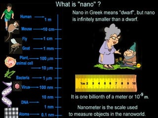
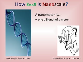
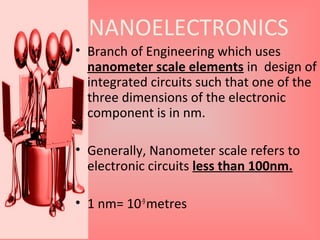
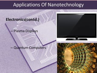
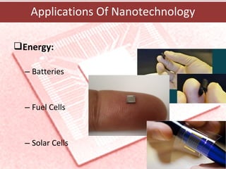
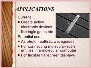
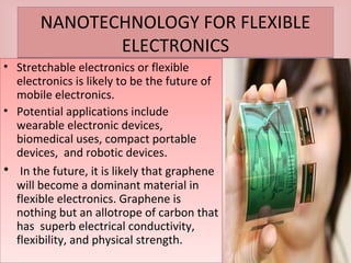
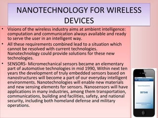
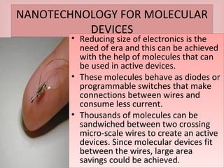
1
Nanoelectronics…
“Nanotechnology is the art and science of
manipulating matter at the nanoscale”
What is NanoNanotechnologytechnology?
A nanometer is…
– one billionth of a meter
How Small Is NanoNanoscale?
Human Hair: Approx. 1x10⁵
nmDNA Sample: Approx. 2 nm
• Branch of Engineering which uses
nanometer scale elements in design of
integrated circuits such that one of the
three dimensions of the electronic
component is in nm.
• Generally, Nanometer scale refers to
electronic circuits less than 100nm.
• 1 nm= 10-9
metres
NANOELECTRONICS
What is Nanoelectronics ?
Nanoelectronics make use of scientific methods at atomic scale for
developing the Nano machines. The main target is to reduce the size, risk
factor and surface areas of the materials and molecules. Machines under
nano electronic process undergoes the long range of manufacturing steps
each with accurate molecular treatment.
Nanoelectronics is one of the major technologies of Nanotechnology.
It plays vital role in the field of engineering and electronics.
Nanoelectronics is one of the major technologies of Nanotechnology.
It plays vital role in the field of engineering and electronics.
What is Nanoelectronics ?-Contd.
The Nanotechnology field has been the subject of intense focus,
particularly from the viewpoint of the electronics industry. The
commitment is, no doubt, driven to a large measure by the current top-
down methodologies for fabrication of silicon-based devices. This is
implied in the next-generation approach towards manufacture of MEMS,
microprocessors, optical switching and several other electronic
components.
Nanotechnology is expected to bring about improvisation in deposition,
implantation, lithography and metrology, thus supporting scaling up of
silicon CMOS and is eventually expected to replace CMOS.
Advantages of Nanoelectronics
One of the obvious advantage is that Nanoelectronics reduces size and
scale of the machine with the help of complex integration on the circuit
silicon chips.
Advanced properties of semiconductors can be determined with the
help of Nanoelectronics.
Molecular scale Nanoelectronics is also known as “the next step” in the
miniaturization of electronic devices, with latest electronics theory and
research in the field of nanoelectronics, it is possible to explore the
diverse properties of molecules.
Extreme fabrication also supported the multiple use of single machine.
Parallel processing is also empowered by Nanoelectronics.
Applications Of
NanoNanotechnology for
Electronics
Electronics:
– Nano Transistors
– Nano Diodes
– OLED (Organic Light Emitting Diode)
Applications Of Nanotechnology
Electronics(contd.)
– Plasma Displays
– Quantum Computers
Applications Of Nanotechnology
Energy:
– Batteries
– Fuel Cells
– Solar Cells
Applications Of Nanotechnology
EJ MOSFET (Electrically variable shallow
junction MOSFET)
NANO MOSFET
SCALING LIMITS OF MOSFET
• Technical problem: For channel length<30nm ,
insulating SiO2 is expected to be less than 2nm
thick. This thin layer causes gate dielectric
tunneling
• Physical problem: For channel length<10nm,
direct source-drain tunneling occurs.
QUANTUM EFFECTS IN ULTRASHORT CHANNEL
MOSFET
• Mobility enhancement due to decrease
in scattering
• Threshold voltage increases with
decrease in channel width
THRESHOLD VOLTAGE ADJUSTMENT USING
QUANTUM EFFECTS
• For <110> oriented device n type has
greater VT shift than p type
• For <100> oriented device p type has
greater VT shift than n type
• To keep VT same for both square
scaling i.e. width = height is used.
BALLISTIC TRANSPORT IN
NANO STRUCTURES
• At room temperature mean free path
of electron is around 10nm.So, at
ultrashort channel length electron
scattering decreases considerably.
• At channel length less than
10nm,scattering approaches zero. It is
called ballistic transport.
• With decrease in temperature mean
free path can be increased & ballistic
transport can be obtained at larger
channel length.
RESONANT TUNNELING IN
NANO DEVICES
• RT is observed in hetero-structure
semiconductor devices made from
pairs of different alloys III-V alloys..
• Eg. AlGaAs/GaAs/AlGaAs diodes
CURRENT APPLICATIONS
In field of electronics & communication
• In solar cells to trap electrons
• Touch screens and flexible displays
• nanoradio, a radio receiver consisting of a
single nanotube, was demonstrated in
2007
• In fabrication of ultracapacitors (which
have high energy density)
NANOWIRES
• Electrons in nanowires are quantum
confined laterally and thus occupy
energy levels that are different from
that in bulk materials.
• Aspect ratios (length-to-width ratio) of
1000 or more
• Poor conductivity (edge effect)
WORLD’S smallest transistor
quantum dot with a tiny
circular cage at the center
known as the central island.
Voltage can change the
conductivity of these
quantum dots, allowing
them to store logic states
Ability to retain conductivity when only one
atom thick.
a small sheet of graphene is taken &
channels are carved into it using electron
beam lithography. What remains is a
Graphene Sheets
NANO RADIO
• A nanoradio is a radio receiver or transmitter
constructed on a nanometer scale.
• Currently only receivers have been developed(
October 2007)
WORKING
• The nanotube, is contained in a
vacuum and one of its ends is
connected to an electrode of a battery.
The other electrode is placed a short
distance from the nanotube's other
end. The tube will vibrate in tune with
any external electromagnetic signal,
effectively acting as an antenna. The
vibration frequency can be adjusted by
changing the applied voltage.
NANO EMISSIVE DISPLAY
• Launched in May,2005 by motorola
• Works by moving electrons through its
driver electronics and into the
nanotubes, which then direct the
electrons at groups of phosphors
(pixels) on the interior surface of the
display. When the phosphors are
bombarded with electrons, they glow,
giving off color—similar to the
operation of a traditional CRT
ADVANTAGES
• Light in weight and more slim
• Saves 20% to 30% more power than other flat
panel displays
• Manufacturing cost is estimated to be a half
to a third the cost of LCD and plasma displays
APPLICATION
• Laptop screen due to better power
saving & size
• Screens in fighter planes due to better
brightness & resolution
• Automotive and aeronautical purposes
• TV displays
WHY ONLY NANOTECHNOLOGY FOR
FUTURE ELECTRONICS?
WHY ONLY NANOTECHNOLOGY FOR
FUTURE ELECTRONICS?
• Today microelectronics are
used and they solve our most
of the problems. Then why do
we need Nanotechnology?
• The two exceptional
disadvantages of micro
electronics are:
 Physical size
 Increasing cost of fabrication
of integrated circuits.
• Today microelectronics are
used and they solve our most
of the problems. Then why do
we need Nanotechnology?
• The two exceptional
disadvantages of micro
electronics are:
 Physical size
 Increasing cost of fabrication
of integrated circuits.
FUTURE SCOPE IN NANOTECHNOLOGYFUTURE SCOPE IN NANOTECHNOLOGY
• Nanotechnology for flexible Electronics
• Nanotechnology for wireless devices
• Nanotechnology for molecular devices
• Nanotechnology for flexible Electronics
• Nanotechnology for wireless devices
• Nanotechnology for molecular devices
NANOTECHNOLOGY FOR FLEXIBLE
ELECTRONICS
NANOTECHNOLOGY FOR FLEXIBLE
ELECTRONICS
• Stretchable electronics or flexible
electronics is likely to be the future of
mobile electronics.
• Potential applications include
wearable electronic devices,
biomedical uses, compact portable
devices, and robotic devices.
• In the future, it is likely that graphene
will become a dominant material in
flexible electronics. Graphene is
nothing but an allotrope of carbon that
has superb electrical conductivity,
flexibility, and physical strength.
NANOTECHNOLOGY FOR WIRELESS
DEVICES
NANOTECHNOLOGY FOR WIRELESS
DEVICES
• Visions of the wireless industry aims at ambient intelligence:
computation and communication always available and ready
to serve the user in an intelligent way.
• All these requirements combined lead to a situation which
cannot be resolved with current technologies.
Nanotechnology could provide solutions for these new
technologies.
• SENSORS- Micromechanical sensors became an elementary
part of automotive technologies in mid 1990, Within next ten
years the development of truly embedded sensors based on
nanostructures will become a part of our everyday intelligent
environments. Nanotechnologies will enable new materials
and new sensing elements for sensors. Nanosensors will have
applications in many industries, among them transportation,
communications, building and facilities, safety, and national
security, including both homeland defense and military
operations.
NANOTECHNOLOGY FOR MOLECULAR
DEVICES
NANOTECHNOLOGY FOR MOLECULAR
DEVICES
• Reducing size of electronics is the
need of era and this can be achieved
with the help of molecules that can
be used in active devices.
• These molecules behave as diodes or
programmable switches that make
connections between wires and
consume less current.
• Thousands of molecules can be
sandwiched between two crossing
micro-scale wires to create an active
devices. Since molecular devices fit
between the wires, large area
savings could be achieved.
• Nanotechnology with all its challenges and opportunities
will become a part of our future.
• The researchers are optimistic for the products based
upon this technology.
• Nanotechnology is slowly but steadily ushering in the
new industrial revolution.
ConclusionConclusion
Thank you!!t

Ele cproject final

  • 1.
  • 3.
    “Nanotechnology is theart and science of manipulating matter at the nanoscale” What is NanoNanotechnologytechnology?
  • 4.
    A nanometer is… –one billionth of a meter How Small Is NanoNanoscale? Human Hair: Approx. 1x10⁵ nmDNA Sample: Approx. 2 nm
  • 5.
    • Branch ofEngineering which uses nanometer scale elements in design of integrated circuits such that one of the three dimensions of the electronic component is in nm. • Generally, Nanometer scale refers to electronic circuits less than 100nm. • 1 nm= 10-9 metres NANOELECTRONICS
  • 6.
    What is Nanoelectronics? Nanoelectronics make use of scientific methods at atomic scale for developing the Nano machines. The main target is to reduce the size, risk factor and surface areas of the materials and molecules. Machines under nano electronic process undergoes the long range of manufacturing steps each with accurate molecular treatment. Nanoelectronics make use of scientific methods at atomic scale for developing the Nano machines. The main target is to reduce the size, risk factor and surface areas of the materials and molecules. Machines under nano electronic process undergoes the long range of manufacturing steps each with accurate molecular treatment. Nanoelectronics is one of the major technologies of Nanotechnology. It plays vital role in the field of engineering and electronics. Nanoelectronics is one of the major technologies of Nanotechnology. It plays vital role in the field of engineering and electronics.
  • 7.
    What is Nanoelectronics?-Contd. The Nanotechnology field has been the subject of intense focus, particularly from the viewpoint of the electronics industry. The commitment is, no doubt, driven to a large measure by the current top- down methodologies for fabrication of silicon-based devices. This is implied in the next-generation approach towards manufacture of MEMS, microprocessors, optical switching and several other electronic components. Nanotechnology is expected to bring about improvisation in deposition, implantation, lithography and metrology, thus supporting scaling up of silicon CMOS and is eventually expected to replace CMOS.
  • 8.
    Advantages of Nanoelectronics Oneof the obvious advantage is that Nanoelectronics reduces size and scale of the machine with the help of complex integration on the circuit silicon chips. Advanced properties of semiconductors can be determined with the help of Nanoelectronics. Molecular scale Nanoelectronics is also known as “the next step” in the miniaturization of electronic devices, with latest electronics theory and research in the field of nanoelectronics, it is possible to explore the diverse properties of molecules. Extreme fabrication also supported the multiple use of single machine. Parallel processing is also empowered by Nanoelectronics.
  • 9.
  • 10.
    Electronics: – Nano Transistors –Nano Diodes – OLED (Organic Light Emitting Diode) Applications Of Nanotechnology
  • 11.
    Electronics(contd.) – Plasma Displays –Quantum Computers Applications Of Nanotechnology
  • 12.
    Energy: – Batteries – FuelCells – Solar Cells Applications Of Nanotechnology
  • 13.
    EJ MOSFET (Electricallyvariable shallow junction MOSFET) NANO MOSFET
  • 14.
    SCALING LIMITS OFMOSFET • Technical problem: For channel length<30nm , insulating SiO2 is expected to be less than 2nm thick. This thin layer causes gate dielectric tunneling • Physical problem: For channel length<10nm, direct source-drain tunneling occurs.
  • 17.
    QUANTUM EFFECTS INULTRASHORT CHANNEL MOSFET • Mobility enhancement due to decrease in scattering • Threshold voltage increases with decrease in channel width
  • 18.
    THRESHOLD VOLTAGE ADJUSTMENTUSING QUANTUM EFFECTS • For <110> oriented device n type has greater VT shift than p type • For <100> oriented device p type has greater VT shift than n type • To keep VT same for both square scaling i.e. width = height is used.
  • 20.
    BALLISTIC TRANSPORT IN NANOSTRUCTURES • At room temperature mean free path of electron is around 10nm.So, at ultrashort channel length electron scattering decreases considerably. • At channel length less than 10nm,scattering approaches zero. It is called ballistic transport. • With decrease in temperature mean free path can be increased & ballistic transport can be obtained at larger channel length.
  • 21.
    RESONANT TUNNELING IN NANODEVICES • RT is observed in hetero-structure semiconductor devices made from pairs of different alloys III-V alloys.. • Eg. AlGaAs/GaAs/AlGaAs diodes
  • 25.
    CURRENT APPLICATIONS In fieldof electronics & communication • In solar cells to trap electrons • Touch screens and flexible displays • nanoradio, a radio receiver consisting of a single nanotube, was demonstrated in 2007 • In fabrication of ultracapacitors (which have high energy density)
  • 26.
    NANOWIRES • Electrons innanowires are quantum confined laterally and thus occupy energy levels that are different from that in bulk materials. • Aspect ratios (length-to-width ratio) of 1000 or more • Poor conductivity (edge effect)
  • 30.
    WORLD’S smallest transistor quantumdot with a tiny circular cage at the center known as the central island. Voltage can change the conductivity of these quantum dots, allowing them to store logic states Ability to retain conductivity when only one atom thick. a small sheet of graphene is taken & channels are carved into it using electron beam lithography. What remains is a Graphene Sheets
  • 33.
    NANO RADIO • Ananoradio is a radio receiver or transmitter constructed on a nanometer scale. • Currently only receivers have been developed( October 2007)
  • 34.
    WORKING • The nanotube,is contained in a vacuum and one of its ends is connected to an electrode of a battery. The other electrode is placed a short distance from the nanotube's other end. The tube will vibrate in tune with any external electromagnetic signal, effectively acting as an antenna. The vibration frequency can be adjusted by changing the applied voltage.
  • 36.
    NANO EMISSIVE DISPLAY •Launched in May,2005 by motorola • Works by moving electrons through its driver electronics and into the nanotubes, which then direct the electrons at groups of phosphors (pixels) on the interior surface of the display. When the phosphors are bombarded with electrons, they glow, giving off color—similar to the operation of a traditional CRT
  • 37.
    ADVANTAGES • Light inweight and more slim • Saves 20% to 30% more power than other flat panel displays • Manufacturing cost is estimated to be a half to a third the cost of LCD and plasma displays
  • 38.
    APPLICATION • Laptop screendue to better power saving & size • Screens in fighter planes due to better brightness & resolution • Automotive and aeronautical purposes • TV displays
  • 39.
    WHY ONLY NANOTECHNOLOGYFOR FUTURE ELECTRONICS? WHY ONLY NANOTECHNOLOGY FOR FUTURE ELECTRONICS? • Today microelectronics are used and they solve our most of the problems. Then why do we need Nanotechnology? • The two exceptional disadvantages of micro electronics are:  Physical size  Increasing cost of fabrication of integrated circuits. • Today microelectronics are used and they solve our most of the problems. Then why do we need Nanotechnology? • The two exceptional disadvantages of micro electronics are:  Physical size  Increasing cost of fabrication of integrated circuits.
  • 40.
    FUTURE SCOPE INNANOTECHNOLOGYFUTURE SCOPE IN NANOTECHNOLOGY • Nanotechnology for flexible Electronics • Nanotechnology for wireless devices • Nanotechnology for molecular devices • Nanotechnology for flexible Electronics • Nanotechnology for wireless devices • Nanotechnology for molecular devices
  • 41.
    NANOTECHNOLOGY FOR FLEXIBLE ELECTRONICS NANOTECHNOLOGYFOR FLEXIBLE ELECTRONICS • Stretchable electronics or flexible electronics is likely to be the future of mobile electronics. • Potential applications include wearable electronic devices, biomedical uses, compact portable devices, and robotic devices. • In the future, it is likely that graphene will become a dominant material in flexible electronics. Graphene is nothing but an allotrope of carbon that has superb electrical conductivity, flexibility, and physical strength. • Stretchable electronics or flexible electronics is likely to be the future of mobile electronics. • Potential applications include wearable electronic devices, biomedical uses, compact portable devices, and robotic devices. • In the future, it is likely that graphene will become a dominant material in flexible electronics. Graphene is nothing but an allotrope of carbon that has superb electrical conductivity, flexibility, and physical strength.
  • 42.
    NANOTECHNOLOGY FOR WIRELESS DEVICES NANOTECHNOLOGYFOR WIRELESS DEVICES • Visions of the wireless industry aims at ambient intelligence: computation and communication always available and ready to serve the user in an intelligent way. • All these requirements combined lead to a situation which cannot be resolved with current technologies. Nanotechnology could provide solutions for these new technologies. • SENSORS- Micromechanical sensors became an elementary part of automotive technologies in mid 1990, Within next ten years the development of truly embedded sensors based on nanostructures will become a part of our everyday intelligent environments. Nanotechnologies will enable new materials and new sensing elements for sensors. Nanosensors will have applications in many industries, among them transportation, communications, building and facilities, safety, and national security, including both homeland defense and military operations. • Visions of the wireless industry aims at ambient intelligence: computation and communication always available and ready to serve the user in an intelligent way. • All these requirements combined lead to a situation which cannot be resolved with current technologies. Nanotechnology could provide solutions for these new technologies. • SENSORS- Micromechanical sensors became an elementary part of automotive technologies in mid 1990, Within next ten years the development of truly embedded sensors based on nanostructures will become a part of our everyday intelligent environments. Nanotechnologies will enable new materials and new sensing elements for sensors. Nanosensors will have applications in many industries, among them transportation, communications, building and facilities, safety, and national security, including both homeland defense and military operations.
  • 43.
    NANOTECHNOLOGY FOR MOLECULAR DEVICES NANOTECHNOLOGYFOR MOLECULAR DEVICES • Reducing size of electronics is the need of era and this can be achieved with the help of molecules that can be used in active devices. • These molecules behave as diodes or programmable switches that make connections between wires and consume less current. • Thousands of molecules can be sandwiched between two crossing micro-scale wires to create an active devices. Since molecular devices fit between the wires, large area savings could be achieved. • Reducing size of electronics is the need of era and this can be achieved with the help of molecules that can be used in active devices. • These molecules behave as diodes or programmable switches that make connections between wires and consume less current. • Thousands of molecules can be sandwiched between two crossing micro-scale wires to create an active devices. Since molecular devices fit between the wires, large area savings could be achieved.
  • 44.
    • Nanotechnology withall its challenges and opportunities will become a part of our future. • The researchers are optimistic for the products based upon this technology. • Nanotechnology is slowly but steadily ushering in the new industrial revolution. ConclusionConclusion
  • 45.

Editor's Notes

  • #4 by definiton as you can see ”it’s the art of manipulating matter at the nanoscale level”
  • #5 1. Its a bit difficult to realize how small the nano-scale is. To make things easier to get, we can say that one nanometre (nm) is one billionth of a metre. -2. Lets see some examples to make it clear In the picture on the right, we can see a man staring at his picked hair trying to figuring out the diameter of it, he will essentially come to the conclusion that a human hair is 100,000nm thick, while a DNA molecule is only 2 nms wide.
  • #10 lets have a look how NT is leading us in different areas of expertise..
  • #11 e.g: in da field of electronics nanotransistors are becoming more nd more popular bcoz of it’s compactness.. If u are thinking that this is a single transistor then you need to reshape your thinking, bcoz this is a transistor box containing thousonds of transistors in it… Some other examples of nanoelectronics are Nanodiodes, OLEDs etc.
  • #12 The aapliances made with the help of nanoelectronics are getting its market share increasing and are becoming popular day by day due to the productivity and quality they have. Such as plasma Displays nd Quantum computing..
  • #13 1-This is a nano-engineered battery, light in weight and flexible just like a paper. It can be rolled, twisted, folded or cut into a number of shapes with absolutely no loss of mechanical efficiency. Other energy suppliment examples with some change in their properties are fuel cells and solar cells