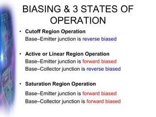
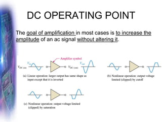
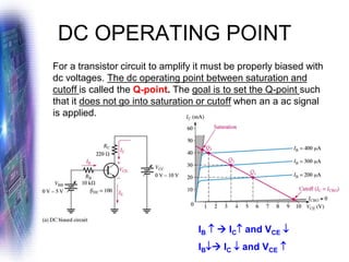
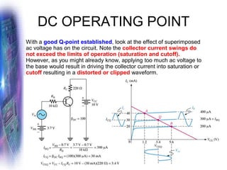
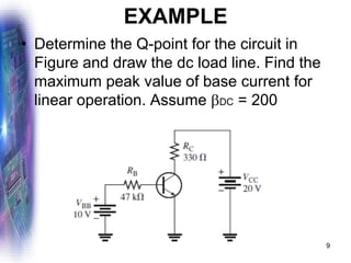
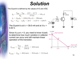
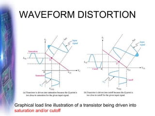
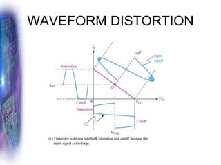
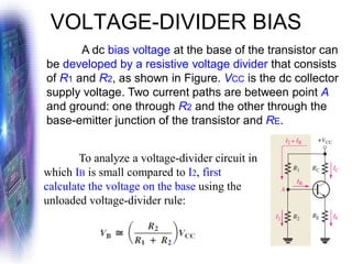
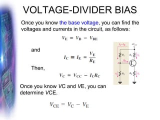
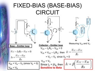
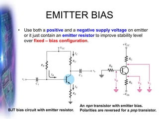
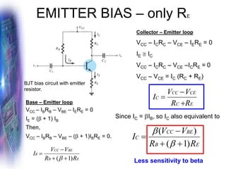
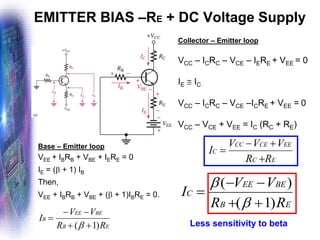
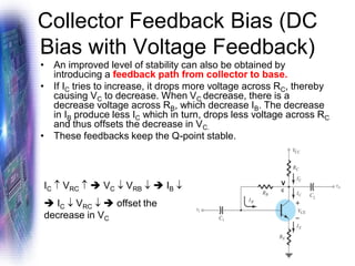
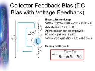
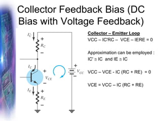
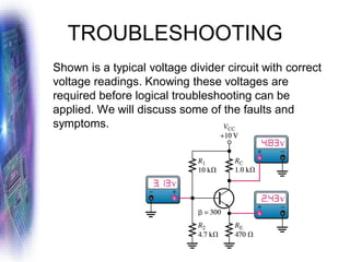
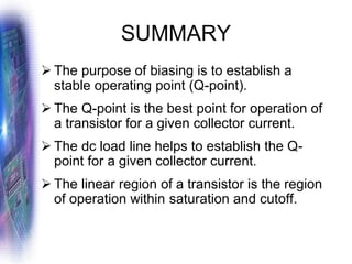
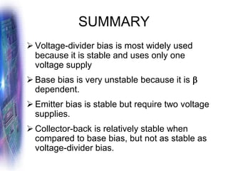
SlideShare a Scribd company logo
1 of 48
Download to read offline
Dr. Awadh Al-Kubati
ELECTRONICS 1
University of Sana’a
Faculty of Engineering
Department of Biomedical Engineering
DC Biasing – Bipolar Junction Transistors
(BJTs)
CHAPTER 4
OBJECTIVES
• Discuss the concept of dc biasing of a transistor
• Analyze voltage-divider bias, base bias, emitter bias
and collector-feedback bias circuits.
• Basic troubleshooting for transistor bias circuits.
INTRODUCTION
• For the transistor to properly operate it must be
biased. There are several methods to establish the
DC operating point.
• We will discuss some of the methods used for
biasing transistors as well as troubleshooting
methods used for transistor bias circuits.
BIASING & 3 STATES OF
OPERATION
• Cutoff Region Operation
Base–Emitter junction is reverse biased
• Active or Linear Region Operation
Base–Emitter junction is forward biased
Base–Collector junction is reverse biased
• Saturation Region Operation
Base–Emitter junction is forward biased
Base–Collector junction is forward biased
DC OPERATING POINT
The goal of amplification in most cases is to increase the
amplitude of an ac signal without altering it.
DC OPERATING POINT
For a transistor circuit to amplify it must be properly biased with
dc voltages. The dc operating point between saturation and
cutoff is called the Q-point. The goal is to set the Q-point such
that it does not go into saturation or cutoff when an a ac signal
is applied.
IB  → IC and VCE 
IB→ IC  and VCE 
DC OPERATING POINT
Recall that the collector characteristic curves graphically show
the relationship of collector current and VCE for different
base currents. With the dc load line superimposed across the
collector curves for this particular transistor we see that 30 mA
(IB = 300 A) of collector current is best for maximum
amplification, giving equal amount above and below the Q-
point. Note that this is three different scenarios of collector
current being viewed simultaneously.
DC OPERATING POINT
With a good Q-point established, look at the effect of superimposed
ac voltage has on the circuit. Note the collector current swings do
not exceed the limits of operation (saturation and cutoff).
However, as you might already know, applying too much ac voltage to
the base would result in driving the collector current into saturation or
cutoff resulting in a distorted or clipped waveform.
EXAMPLE
• Determine the Q-point for the circuit in
Figure and draw the dc load line. Find the
maximum peak value of base current for
linear operation. Assume DC = 200
9
Solution
• The Q-point is defined by the values of IC and VCE.
10
The Q-point is at IC = 39.6 mA and at VCE =
6.93 V.
Since IC(cutoff ) = 0, you need to know IC(sat)
to determine how much variation in collector
current can occur and still maintain linear
operation of the transistor.
WAVEFORM DISTORTION
Graphical load line illustration of a transistor being driven into
saturation and/or cutoff
WAVEFORM DISTORTION
VOLTAGE-DIVIDER BIAS
A dc bias voltage at the base of the transistor can
be developed by a resistive voltage divider that consists
of R1 and R2, as shown in Figure. VCC is the dc collector
supply voltage. Two current paths are between point A
and ground: one through R2 and the other through the
base-emitter junction of the transistor and RE.
To analyze a voltage-divider circuit in
which IB is small compared to I2, first
calculate the voltage on the base using the
unloaded voltage-divider rule:
VOLTAGE-DIVIDER BIAS
Once you know the base voltage, you can find the
voltages and currents in the circuit, as follows:
Once you know VC and VE, you can
determine VCE.
and
Then,
EXAMPLE
Determine VCE and IC in the stiff voltage-divider biased
transistor circuit of Figure if DC = 100.
Solution The base voltage is
Thevenin’s Theorem Applied
to Voltage-Divider Bias
To analyze a voltage-divider biased transistor circuit for
base current loading effects, we will apply Thevenin’s
theorem to evaluate the circuit.
and the resistance is
Thevenin’s Theorem Applied to
Voltage-Divider Bias
Applying Kirchhoff’s voltage law around the equivalent base-emitter loop
gives
Substituting, using Ohm’s law, and solving for VTH,
Substituting IE / DC for IB,
Then solving for IE,
FIXED-BIAS (BASE-BIAS)
CIRCUIT
• Simplest transistor bias configuration.
• Commonly used in relay driver circuits.
• Extremely beta-dependant and very unstable
Fixed-bias circuit. DC equivalent circuit.
FIXED-BIAS (BASE-BIAS)
CIRCUIT





 −
=
B
BE
CC
C
R
V
V
I 
VCC – ICRC – VCE = 0
VCE = VCC – ICRC; then
= VC – VE since VE = 0
VCE = VC
Measuring VCE and VC.
Since IC = IB, then
C
CE
CC
C
R
V
V
I
−
=
B
BE
CC
B
BE
B
B
CC
R
V
V
I
V
R
I
V
−
=
=
−
− 0
VBE = VB – VE (since VE = 0)
VBE = VB
Base – Emitter loop Collector – Emitter loop
Sensitive to Beta
EMITTER BIAS
• Use both a positive and a negative supply voltage on emitter
or it just contain an emitter resistor to improve stability level
over fixed – bias configuration.
BJT bias circuit with emitter resistor.
An npn transistor with emitter bias.
Polarities are reversed for a pnp transistor.
EMITTER BIAS – only RE
Collector – Emitter loop
VCC – ICRC – VCE – IERE = 0
IE  IC
VCC – ICRC – VCE –ICRE = 0
VCC – VCE = IC (RC + RE)
E
B
BE
CC
B
R
R
V
V
I
)
1
( +
+
−
=

E
B
BE
CC
C
R
R
V
V
I
)
1
(
)
(
+
+
−
=


BJT bias circuit with emitter
resistor.
Base – Emitter loop
VCC – IBRB – VBE – IERE = 0
IE = ( + 1) IB
Then,
VCC – IBRB – VBE – ( + 1)IBRE = 0.
Less sensitivity to beta
Since IC = IB, so IC also equivalent to
E
C
CE
CC
C
R
R
V
V
I
+
−
=
EMITTER BIAS –RE + DC Voltage Supply
E
B
BE
EE
B
R
R
V
V
I
)
1
( +
+
−
−
=

E
C
EE
CE
CC
C
R
R
V
V
V
I
+
+
−
=
Base – Emitter loop
VEE + IBRB + VBE + IERE = 0
IE = ( + 1) IB
Then,
VEE + IBRB + VBE + ( + 1)IBRE = 0.
Less sensitivity to beta
E
B
BE
EE
C
R
R
V
V
I
)
1
(
)
(
+
+
−
−
=


Collector – Emitter loop
VCC – ICRC – VCE – IERE + VEE = 0
IE  IC
VCC – ICRC – VCE –ICRE + VEE = 0
VCC – VCE + VEE = IC (RC + RE)
EMITTER BIAS - Summary
With DC Voltage supply + Resistor at Emitter
E
B
BE
EE
C
R
R
V
V
I
)
1
(
)
(
+
+
−
−
=


E
B
BE
EE
C
R
R
V
V
I
+
−
−


E
B
BE
CC
C
R
R
V
V
I
)
1
(
)
(
+
+
−
=


Less sensitivity to beta
or independent to beta
With only Resistor at Emitter
Previous analysis we use IE = ( + 1) IB; but if use IE  IC  IB, then
from previous slide we can get.
OR we also can use
 ( + 1) to get the
same result.
If RE >>> RB/ then we can drop RB/
in equation
E
BE
EE
C
R
V
V
I
−
−

If VEE >>> VBE then
E
EE
C
R
V
I
−
 Independent to VBE
EXAMPLE
Determine VCEQ and IE for
the network as shown in Fig.
VEE – IBRB – VBE – IERE = 0
IE = ( + 1)IB
A
I
k
k
V
V
I
R
R
V
V
I
B
B
E
B
BE
EE
B


73
.
45
)
2
)(
91
(
240
7
.
0
20
)
1
(
=
+

−
=
+
+
−
=
-VEE + IERE + VCE = 0
IE = ( + 1)IB
VCEQ = VEE – (+1) IBRE
= 20V – (91)(45.73)(2k)
= 11.68 mA
IE = 4.16 mA
EXAMPLE
Calculate IE and VCE for the circuit in Figure using
the approximations VE = -1 V and IC = IE.
EMITTER BIAS - Summary
• Adding RE to the emitter improves
the stability of a transistor.
• Stability refers to a bias circuit in which the
currents and voltages will remain fairly
constant for a wide range of temperatures
and transistor Beta () values.
VOLTAGE DIVIDER BIAS
• The most widely used type of bias circuit. Only one power
supply is needed and voltage-divider bias is more stable (
independent) than other bias types.
• Two methods of analysis, exact and approximate analysis
VOLTAGE DIVIDER BIAS –
Exact Analysis
Determining RTH.
To determine RTH → The voltage source is replaced by a short-
circuit equivalent, resulting……..
RTH = R1 ǁ R2
VOLTAGE DIVIDER BIAS –
Exact Analysis
To determine ETH → The
voltage source VCC remained
on the network and the open
circuit Thevenin voltage can be
determined.
Determining ETH.
2
1
2
2
R
R
R
V
V
E
CC
R
TH
+
=
=
VOLTAGE DIVIDER BIAS –
Exact Analysis
The Thevenin network
is then redrawn and IBQ
can be determined by
applying Kirchoff’s
voltage law.
ETH – IBRTH – VBE – IERE = 0,
….substitute IE = ( + 1) IB….. then
E
TH
BE
TH
B
R
R
V
E
I
)
1
( +
+
−
=

Almost similar with emitter bias
Voltage differences over resistance.
VOLTAGE DIVIDER BIAS –
Exact Analysis

/
TH
E
BE
TH
E
R
R
V
E
I
+
−
=
IC = IB ; IE = ( + 1) IB  IB
Substituting between these OR
equation in previous slide (from
derivation), resulting :
E
TH
BE
TH
B
R
R
V
E
I
)
1
( +
+
−
=

If RE >>> RTH/, then…
E
BE
TH
E
R
V
E
I
−
=
Independent to Beta
VOLTAGE DIVIDER BIAS –
Exact Analysis
Voltage-divider bias configuration.
Once IB is known, the rest
of the parameters can be
determined.
VCE = VCC – IC (RC + RE)
The remaining equations
VE, VC and VB are also
similar as obtained in
emitter bias configuration.
VOLTAGE DIVIDER BIAS –
Approximate Analysis
Partial-bias circuit for calculating the
approximate base voltage VB.
2
1
2
R
R
V
R
V
CC
B
+
=
and
Ri = ( + 1)RE  RE
with condition
RE  10R2
If beta times the value RE is at
least 10x the value R2, the
approximate approach can be
applied with high accuracy.
Ri = equivalent
transistor between
base and ground for
transistor with an
emitter resistor RE
VOLTAGE DIVIDER BIAS –
Approximate Analysis
Partial-bias circuit for calculating the
approximate base voltage VB.
Once VB is determined,
the level of VE can be
calculated.
VE = VB – VBE
And emitter current
and IC  IE
VCE = VCC –ICRC –IERE but
since IE  IC
VCE= VCC – IE (RC + RE)
E
E
E
R
V
I =
Collector Feedback Bias (DC
Bias with Voltage Feedback)
• An improved level of stability can also be obtained by
introducing a feedback path from collector to base.
• If IC tries to increase, it drops more voltage across RC, thereby
causing VC to decrease. When VC decrease, there is a
decrease voltage across RB, which decrease IB. The decrease
in IB produce less IC which in turn, drops less voltage across RC
and thus offsets the decrease in VC.
• These feedbacks keep the Q-point stable.
V
C
IC  VRC  ➔ VC  VRB  ➔ IB 
➔ IC  VRC  ➔ offset the
decrease in VC
Collector Feedback Bias (DC
Bias with Voltage Feedback)
Base – Emitter Loop
VCC – IC'RC – IBRB – VBE – IERE = 0
Actual case IC' = IC + IB
Approximation can be employed :
IC'  IC = IB and IE  IC
VCC – VBE - IB (RC + RE) – IBRB = 0
Solving for IB, yields
)
( E
C
B
BE
CC
B
R
R
R
V
V
I
+
+
−
=

Collector Feedback Bias (DC
Bias with Voltage Feedback)
Collector – Emitter Loop
VCC – IC'RC – VCE – IERE = 0
Approximation can be employed :
IC'  IC and IE  IC
VCC – VCE - IC (RC + RE) = 0
VCE = VCC – IC (RC + RE)
TROUBLESHOOTING
Shown is a typical voltage divider circuit with correct
voltage readings. Knowing these voltages are
required before logical troubleshooting can be
applied. We will discuss some of the faults and
symptoms.
TROUBLESHOOTING
R1 Open
With no bias the
transistor is in
cutoff.
Base voltage goes
down to 0V.
Collector voltage
goes up to 10 V
(VCC).
Emitter voltage goes
down to 0V.
TROUBLESHOOTING
Resistor RE Open:
Transistor is in cutoff.
Base reading voltage will
stay approximately the
same.
Collector voltage goes up
to 10V(VCC).
Emitter voltage will be
approximately the base
voltage + 0.7V.
TROUBLESHOOTING
Base Open Internally:
Transistor is in cutoff.
Base voltage stays
approximately the
same.
Collector voltage goes
up to 10V(VCC).
Emitter voltage goes
down to 0V.
TROUBLESHOOTING
Open BE Junction:
Transistor is in cutoff.
Base voltage stays
approximately the
same.
Collector voltage goes
up to 10V(VCC)
Emitter voltage goes
down to 0V.
TROUBLESHOOTING
Open BC Junction:
Base voltage goes down
to 1.11V because of
more base current flow
through emitter.
Collector voltage goes
up to 10V (VCC).
Emitter voltage will drop
to 0.41V because of
small current flow from
forward biased base-
emitter junction.
TROUBLESHOOTING
RC Open:
Base voltage goes down to
1.11V because of more
current flow through the
emitter.
Collector voltage will drop
to 0.41V because of current
flow from forward biased
collector-base junction.
Emitter voltage will drop to
0.41V because of small
current flow from forward
biased base-emitter
junction.
TROUBLESHOOTING
R2 Open:
Transistor pushed close to
or into saturation.
Base voltage goes up
slightly to 3.83V because
of increased bias.
Emitter voltage goes up to
3.13V because of
increased current.
Collector voltage goes
down because of
increased conduction of
transistor.
SUMMARY
➢ The purpose of biasing is to establish a
stable operating point (Q-point).
➢ The Q-point is the best point for operation of
a transistor for a given collector current.
➢ The dc load line helps to establish the Q-
point for a given collector current.
➢ The linear region of a transistor is the region
of operation within saturation and cutoff.
SUMMARY
➢ Voltage-divider bias is most widely used
because it is stable and uses only one
voltage supply
➢ Base bias is very unstable because it is 
dependent.
➢ Emitter bias is stable but require two voltage
supplies.
➢ Collector-back is relatively stable when
compared to base bias, but not as stable as
voltage-divider bias.
The End
Any Questions ?

More Related Content

Similar to DC Biasing – Bipolar Junction Transistors (BJTs)

Bipolar junction transistor characterstics biassing and amplification, lab 9
Bipolar junction transistor characterstics biassing and amplification, lab 9Bipolar junction transistor characterstics biassing and amplification, lab 9
Bipolar junction transistor characterstics biassing and amplification, lab 9kehali Haileselassie
 
Mba admssion in india
Mba admssion in indiaMba admssion in india
Mba admssion in indiaEdhole.com
 
Transistors handout
Transistors handoutTransistors handout
Transistors handoutEng Mahamed
 
Bipolar junction transistor : Biasing and AC Analysis
Bipolar junction transistor : Biasing and AC AnalysisBipolar junction transistor : Biasing and AC Analysis
Bipolar junction transistor : Biasing and AC AnalysisTahmina Zebin
 
L07 dc and ac load line
L07 dc and ac load lineL07 dc and ac load line
L07 dc and ac load lineHasaan Mehfooz
 
Lecture 06 transistorremodel
Lecture 06 transistorremodelLecture 06 transistorremodel
Lecture 06 transistorremodelIsmael Cayo Apaza
 
Multisim_simulation_project_3_^0_4[1]-2.pptx
Multisim_simulation_project_3_^0_4[1]-2.pptxMultisim_simulation_project_3_^0_4[1]-2.pptx
Multisim_simulation_project_3_^0_4[1]-2.pptxwencove9
 
Phy 4240 lec (9) and (10)
Phy 4240 lec (9) and (10)Phy 4240 lec (9) and (10)
Phy 4240 lec (9) and (10)Dr. Abeer Kamal
 
Transistor cb cc ce power point transistor
Transistor cb cc ce power point transistorTransistor cb cc ce power point transistor
Transistor cb cc ce power point transistor2004akkuu
 
L10 bjt introduction s21617
L10 bjt introduction s21617L10 bjt introduction s21617
L10 bjt introduction s21617Muhammad Fiaz
 
Chapter-6 DC biasing-1.ppt
Chapter-6 DC biasing-1.pptChapter-6 DC biasing-1.ppt
Chapter-6 DC biasing-1.pptJeelBhanderi4
 
Electronics 1 : Chapter # 06 : Bipolar Junction Transistor
Electronics 1 : Chapter # 06 : Bipolar Junction TransistorElectronics 1 : Chapter # 06 : Bipolar Junction Transistor
Electronics 1 : Chapter # 06 : Bipolar Junction TransistorSk_Group
 

Similar to DC Biasing – Bipolar Junction Transistors (BJTs) (20)

Bipolar junction transistor characterstics biassing and amplification, lab 9
Bipolar junction transistor characterstics biassing and amplification, lab 9Bipolar junction transistor characterstics biassing and amplification, lab 9
Bipolar junction transistor characterstics biassing and amplification, lab 9
 
bjt ppt project.ppt
bjt ppt  project.pptbjt ppt  project.ppt
bjt ppt project.ppt
 
Transistor 1 lecture
Transistor 1 lectureTransistor 1 lecture
Transistor 1 lecture
 
Mba admssion in india
Mba admssion in indiaMba admssion in india
Mba admssion in india
 
Transistors.ppt
Transistors.pptTransistors.ppt
Transistors.ppt
 
Transistors handout
Transistors handoutTransistors handout
Transistors handout
 
Ce amplifiers
Ce amplifiersCe amplifiers
Ce amplifiers
 
Bipolar junction transistor : Biasing and AC Analysis
Bipolar junction transistor : Biasing and AC AnalysisBipolar junction transistor : Biasing and AC Analysis
Bipolar junction transistor : Biasing and AC Analysis
 
L07 dc and ac load line
L07 dc and ac load lineL07 dc and ac load line
L07 dc and ac load line
 
Lecture 06 transistorremodel
Lecture 06 transistorremodelLecture 06 transistorremodel
Lecture 06 transistorremodel
 
dc biasing
dc biasingdc biasing
dc biasing
 
Multisim_simulation_project_3_^0_4[1]-2.pptx
Multisim_simulation_project_3_^0_4[1]-2.pptxMultisim_simulation_project_3_^0_4[1]-2.pptx
Multisim_simulation_project_3_^0_4[1]-2.pptx
 
Chapter 1 ac analysis SKEE 2253
Chapter 1 ac analysis SKEE 2253Chapter 1 ac analysis SKEE 2253
Chapter 1 ac analysis SKEE 2253
 
Phy 4240 lec (9) and (10)
Phy 4240 lec (9) and (10)Phy 4240 lec (9) and (10)
Phy 4240 lec (9) and (10)
 
Transistor cb cc ce power point transistor
Transistor cb cc ce power point transistorTransistor cb cc ce power point transistor
Transistor cb cc ce power point transistor
 
L10 bjt introduction s21617
L10 bjt introduction s21617L10 bjt introduction s21617
L10 bjt introduction s21617
 
Chapter-6 DC biasing-1.ppt
Chapter-6 DC biasing-1.pptChapter-6 DC biasing-1.ppt
Chapter-6 DC biasing-1.ppt
 
Electronics 1 : Chapter # 06 : Bipolar Junction Transistor
Electronics 1 : Chapter # 06 : Bipolar Junction TransistorElectronics 1 : Chapter # 06 : Bipolar Junction Transistor
Electronics 1 : Chapter # 06 : Bipolar Junction Transistor
 
Chapter 9
Chapter 9Chapter 9
Chapter 9
 
ELECTRONICS DEVICES AND CIRCUITS
ELECTRONICS DEVICES AND CIRCUITSELECTRONICS DEVICES AND CIRCUITS
ELECTRONICS DEVICES AND CIRCUITS
 

Recently uploaded

OSVC_Meta-Data based Simulation Automation to overcome Verification Challenge...
OSVC_Meta-Data based Simulation Automation to overcome Verification Challenge...OSVC_Meta-Data based Simulation Automation to overcome Verification Challenge...
OSVC_Meta-Data based Simulation Automation to overcome Verification Challenge...Soham Mondal
 
Heart Disease Prediction using machine learning.pptx
Heart Disease Prediction using machine learning.pptxHeart Disease Prediction using machine learning.pptx
Heart Disease Prediction using machine learning.pptxPoojaBan
 
Software and Systems Engineering Standards: Verification and Validation of Sy...
Software and Systems Engineering Standards: Verification and Validation of Sy...Software and Systems Engineering Standards: Verification and Validation of Sy...
Software and Systems Engineering Standards: Verification and Validation of Sy...VICTOR MAESTRE RAMIREZ
 
chaitra-1.pptx fake news detection using machine learning
chaitra-1.pptx  fake news detection using machine learningchaitra-1.pptx  fake news detection using machine learning
chaitra-1.pptx fake news detection using machine learningmisbanausheenparvam
 
Sachpazis Costas: Geotechnical Engineering: A student's Perspective Introduction
Sachpazis Costas: Geotechnical Engineering: A student's Perspective IntroductionSachpazis Costas: Geotechnical Engineering: A student's Perspective Introduction
Sachpazis Costas: Geotechnical Engineering: A student's Perspective IntroductionDr.Costas Sachpazis
 
Gfe Mayur Vihar Call Girls Service WhatsApp -> 9999965857 Available 24x7 ^ De...
Gfe Mayur Vihar Call Girls Service WhatsApp -> 9999965857 Available 24x7 ^ De...Gfe Mayur Vihar Call Girls Service WhatsApp -> 9999965857 Available 24x7 ^ De...
Gfe Mayur Vihar Call Girls Service WhatsApp -> 9999965857 Available 24x7 ^ De...srsj9000
 
main PPT.pptx of girls hostel security using rfid
main PPT.pptx of girls hostel security using rfidmain PPT.pptx of girls hostel security using rfid
main PPT.pptx of girls hostel security using rfidNikhilNagaraju
 
Architect Hassan Khalil Portfolio for 2024
Architect Hassan Khalil Portfolio for 2024Architect Hassan Khalil Portfolio for 2024
Architect Hassan Khalil Portfolio for 2024hassan khalil
 
GDSC ASEB Gen AI study jams presentation
GDSC ASEB Gen AI study jams presentationGDSC ASEB Gen AI study jams presentation
GDSC ASEB Gen AI study jams presentationGDSCAESB
 
Current Transformer Drawing and GTP for MSETCL
Current Transformer Drawing and GTP for MSETCLCurrent Transformer Drawing and GTP for MSETCL
Current Transformer Drawing and GTP for MSETCLDeelipZope
 
Study on Air-Water & Water-Water Heat Exchange in a Finned Tube Exchanger
Study on Air-Water & Water-Water Heat Exchange in a Finned Tube ExchangerStudy on Air-Water & Water-Water Heat Exchange in a Finned Tube Exchanger
Study on Air-Water & Water-Water Heat Exchange in a Finned Tube ExchangerAnamika Sarkar
 
INFLUENCE OF NANOSILICA ON THE PROPERTIES OF CONCRETE
INFLUENCE OF NANOSILICA ON THE PROPERTIES OF CONCRETEINFLUENCE OF NANOSILICA ON THE PROPERTIES OF CONCRETE
INFLUENCE OF NANOSILICA ON THE PROPERTIES OF CONCRETEroselinkalist12
 
Gurgaon ✡️9711147426✨Call In girls Gurgaon Sector 51 escort service
Gurgaon ✡️9711147426✨Call In girls Gurgaon Sector 51 escort serviceGurgaon ✡️9711147426✨Call In girls Gurgaon Sector 51 escort service
Gurgaon ✡️9711147426✨Call In girls Gurgaon Sector 51 escort servicejennyeacort
 
CCS355 Neural Network & Deep Learning Unit II Notes with Question bank .pdf
CCS355 Neural Network & Deep Learning Unit II Notes with Question bank .pdfCCS355 Neural Network & Deep Learning Unit II Notes with Question bank .pdf
CCS355 Neural Network & Deep Learning Unit II Notes with Question bank .pdfAsst.prof M.Gokilavani
 
Concrete Mix Design - IS 10262-2019 - .pptx
Concrete Mix Design - IS 10262-2019 - .pptxConcrete Mix Design - IS 10262-2019 - .pptx
Concrete Mix Design - IS 10262-2019 - .pptxKartikeyaDwivedi3
 
Call Girls Delhi {Jodhpur} 9711199012 high profile service
Call Girls Delhi {Jodhpur} 9711199012 high profile serviceCall Girls Delhi {Jodhpur} 9711199012 high profile service
Call Girls Delhi {Jodhpur} 9711199012 high profile servicerehmti665
 
Biology for Computer Engineers Course Handout.pptx
Biology for Computer Engineers Course Handout.pptxBiology for Computer Engineers Course Handout.pptx
Biology for Computer Engineers Course Handout.pptxDeepakSakkari2
 
APPLICATIONS-AC/DC DRIVES-OPERATING CHARACTERISTICS
APPLICATIONS-AC/DC DRIVES-OPERATING CHARACTERISTICSAPPLICATIONS-AC/DC DRIVES-OPERATING CHARACTERISTICS
APPLICATIONS-AC/DC DRIVES-OPERATING CHARACTERISTICSKurinjimalarL3
 

Recently uploaded (20)

OSVC_Meta-Data based Simulation Automation to overcome Verification Challenge...
OSVC_Meta-Data based Simulation Automation to overcome Verification Challenge...OSVC_Meta-Data based Simulation Automation to overcome Verification Challenge...
OSVC_Meta-Data based Simulation Automation to overcome Verification Challenge...
 
9953056974 Call Girls In South Ex, Escorts (Delhi) NCR.pdf
9953056974 Call Girls In South Ex, Escorts (Delhi) NCR.pdf9953056974 Call Girls In South Ex, Escorts (Delhi) NCR.pdf
9953056974 Call Girls In South Ex, Escorts (Delhi) NCR.pdf
 
Heart Disease Prediction using machine learning.pptx
Heart Disease Prediction using machine learning.pptxHeart Disease Prediction using machine learning.pptx
Heart Disease Prediction using machine learning.pptx
 
Software and Systems Engineering Standards: Verification and Validation of Sy...
Software and Systems Engineering Standards: Verification and Validation of Sy...Software and Systems Engineering Standards: Verification and Validation of Sy...
Software and Systems Engineering Standards: Verification and Validation of Sy...
 
chaitra-1.pptx fake news detection using machine learning
chaitra-1.pptx  fake news detection using machine learningchaitra-1.pptx  fake news detection using machine learning
chaitra-1.pptx fake news detection using machine learning
 
Sachpazis Costas: Geotechnical Engineering: A student's Perspective Introduction
Sachpazis Costas: Geotechnical Engineering: A student's Perspective IntroductionSachpazis Costas: Geotechnical Engineering: A student's Perspective Introduction
Sachpazis Costas: Geotechnical Engineering: A student's Perspective Introduction
 
Gfe Mayur Vihar Call Girls Service WhatsApp -> 9999965857 Available 24x7 ^ De...
Gfe Mayur Vihar Call Girls Service WhatsApp -> 9999965857 Available 24x7 ^ De...Gfe Mayur Vihar Call Girls Service WhatsApp -> 9999965857 Available 24x7 ^ De...
Gfe Mayur Vihar Call Girls Service WhatsApp -> 9999965857 Available 24x7 ^ De...
 
main PPT.pptx of girls hostel security using rfid
main PPT.pptx of girls hostel security using rfidmain PPT.pptx of girls hostel security using rfid
main PPT.pptx of girls hostel security using rfid
 
Architect Hassan Khalil Portfolio for 2024
Architect Hassan Khalil Portfolio for 2024Architect Hassan Khalil Portfolio for 2024
Architect Hassan Khalil Portfolio for 2024
 
GDSC ASEB Gen AI study jams presentation
GDSC ASEB Gen AI study jams presentationGDSC ASEB Gen AI study jams presentation
GDSC ASEB Gen AI study jams presentation
 
Current Transformer Drawing and GTP for MSETCL
Current Transformer Drawing and GTP for MSETCLCurrent Transformer Drawing and GTP for MSETCL
Current Transformer Drawing and GTP for MSETCL
 
young call girls in Rajiv Chowk🔝 9953056974 🔝 Delhi escort Service
young call girls in Rajiv Chowk🔝 9953056974 🔝 Delhi escort Serviceyoung call girls in Rajiv Chowk🔝 9953056974 🔝 Delhi escort Service
young call girls in Rajiv Chowk🔝 9953056974 🔝 Delhi escort Service
 
Study on Air-Water & Water-Water Heat Exchange in a Finned Tube Exchanger
Study on Air-Water & Water-Water Heat Exchange in a Finned Tube ExchangerStudy on Air-Water & Water-Water Heat Exchange in a Finned Tube Exchanger
Study on Air-Water & Water-Water Heat Exchange in a Finned Tube Exchanger
 
INFLUENCE OF NANOSILICA ON THE PROPERTIES OF CONCRETE
INFLUENCE OF NANOSILICA ON THE PROPERTIES OF CONCRETEINFLUENCE OF NANOSILICA ON THE PROPERTIES OF CONCRETE
INFLUENCE OF NANOSILICA ON THE PROPERTIES OF CONCRETE
 
Gurgaon ✡️9711147426✨Call In girls Gurgaon Sector 51 escort service
Gurgaon ✡️9711147426✨Call In girls Gurgaon Sector 51 escort serviceGurgaon ✡️9711147426✨Call In girls Gurgaon Sector 51 escort service
Gurgaon ✡️9711147426✨Call In girls Gurgaon Sector 51 escort service
 
CCS355 Neural Network & Deep Learning Unit II Notes with Question bank .pdf
CCS355 Neural Network & Deep Learning Unit II Notes with Question bank .pdfCCS355 Neural Network & Deep Learning Unit II Notes with Question bank .pdf
CCS355 Neural Network & Deep Learning Unit II Notes with Question bank .pdf
 
Concrete Mix Design - IS 10262-2019 - .pptx
Concrete Mix Design - IS 10262-2019 - .pptxConcrete Mix Design - IS 10262-2019 - .pptx
Concrete Mix Design - IS 10262-2019 - .pptx
 
Call Girls Delhi {Jodhpur} 9711199012 high profile service
Call Girls Delhi {Jodhpur} 9711199012 high profile serviceCall Girls Delhi {Jodhpur} 9711199012 high profile service
Call Girls Delhi {Jodhpur} 9711199012 high profile service
 
Biology for Computer Engineers Course Handout.pptx
Biology for Computer Engineers Course Handout.pptxBiology for Computer Engineers Course Handout.pptx
Biology for Computer Engineers Course Handout.pptx
 
APPLICATIONS-AC/DC DRIVES-OPERATING CHARACTERISTICS
APPLICATIONS-AC/DC DRIVES-OPERATING CHARACTERISTICSAPPLICATIONS-AC/DC DRIVES-OPERATING CHARACTERISTICS
APPLICATIONS-AC/DC DRIVES-OPERATING CHARACTERISTICS
 

DC Biasing – Bipolar Junction Transistors (BJTs)

  • 1. Dr. Awadh Al-Kubati ELECTRONICS 1 University of Sana’a Faculty of Engineering Department of Biomedical Engineering DC Biasing – Bipolar Junction Transistors (BJTs) CHAPTER 4
  • 2. OBJECTIVES • Discuss the concept of dc biasing of a transistor • Analyze voltage-divider bias, base bias, emitter bias and collector-feedback bias circuits. • Basic troubleshooting for transistor bias circuits.
  • 3. INTRODUCTION • For the transistor to properly operate it must be biased. There are several methods to establish the DC operating point. • We will discuss some of the methods used for biasing transistors as well as troubleshooting methods used for transistor bias circuits.
  • 4. BIASING & 3 STATES OF OPERATION • Cutoff Region Operation Base–Emitter junction is reverse biased • Active or Linear Region Operation Base–Emitter junction is forward biased Base–Collector junction is reverse biased • Saturation Region Operation Base–Emitter junction is forward biased Base–Collector junction is forward biased
  • 5. DC OPERATING POINT The goal of amplification in most cases is to increase the amplitude of an ac signal without altering it.
  • 6. DC OPERATING POINT For a transistor circuit to amplify it must be properly biased with dc voltages. The dc operating point between saturation and cutoff is called the Q-point. The goal is to set the Q-point such that it does not go into saturation or cutoff when an a ac signal is applied. IB  → IC and VCE  IB→ IC  and VCE 
  • 7. DC OPERATING POINT Recall that the collector characteristic curves graphically show the relationship of collector current and VCE for different base currents. With the dc load line superimposed across the collector curves for this particular transistor we see that 30 mA (IB = 300 A) of collector current is best for maximum amplification, giving equal amount above and below the Q- point. Note that this is three different scenarios of collector current being viewed simultaneously.
  • 8. DC OPERATING POINT With a good Q-point established, look at the effect of superimposed ac voltage has on the circuit. Note the collector current swings do not exceed the limits of operation (saturation and cutoff). However, as you might already know, applying too much ac voltage to the base would result in driving the collector current into saturation or cutoff resulting in a distorted or clipped waveform.
  • 9. EXAMPLE • Determine the Q-point for the circuit in Figure and draw the dc load line. Find the maximum peak value of base current for linear operation. Assume DC = 200 9
  • 10. Solution • The Q-point is defined by the values of IC and VCE. 10 The Q-point is at IC = 39.6 mA and at VCE = 6.93 V. Since IC(cutoff ) = 0, you need to know IC(sat) to determine how much variation in collector current can occur and still maintain linear operation of the transistor.
  • 11. WAVEFORM DISTORTION Graphical load line illustration of a transistor being driven into saturation and/or cutoff
  • 13. VOLTAGE-DIVIDER BIAS A dc bias voltage at the base of the transistor can be developed by a resistive voltage divider that consists of R1 and R2, as shown in Figure. VCC is the dc collector supply voltage. Two current paths are between point A and ground: one through R2 and the other through the base-emitter junction of the transistor and RE. To analyze a voltage-divider circuit in which IB is small compared to I2, first calculate the voltage on the base using the unloaded voltage-divider rule:
  • 14. VOLTAGE-DIVIDER BIAS Once you know the base voltage, you can find the voltages and currents in the circuit, as follows: Once you know VC and VE, you can determine VCE. and Then,
  • 15. EXAMPLE Determine VCE and IC in the stiff voltage-divider biased transistor circuit of Figure if DC = 100. Solution The base voltage is
  • 16. Thevenin’s Theorem Applied to Voltage-Divider Bias To analyze a voltage-divider biased transistor circuit for base current loading effects, we will apply Thevenin’s theorem to evaluate the circuit. and the resistance is
  • 17. Thevenin’s Theorem Applied to Voltage-Divider Bias Applying Kirchhoff’s voltage law around the equivalent base-emitter loop gives Substituting, using Ohm’s law, and solving for VTH, Substituting IE / DC for IB, Then solving for IE,
  • 18. FIXED-BIAS (BASE-BIAS) CIRCUIT • Simplest transistor bias configuration. • Commonly used in relay driver circuits. • Extremely beta-dependant and very unstable Fixed-bias circuit. DC equivalent circuit.
  • 19. FIXED-BIAS (BASE-BIAS) CIRCUIT       − = B BE CC C R V V I  VCC – ICRC – VCE = 0 VCE = VCC – ICRC; then = VC – VE since VE = 0 VCE = VC Measuring VCE and VC. Since IC = IB, then C CE CC C R V V I − = B BE CC B BE B B CC R V V I V R I V − = = − − 0 VBE = VB – VE (since VE = 0) VBE = VB Base – Emitter loop Collector – Emitter loop Sensitive to Beta
  • 20. EMITTER BIAS • Use both a positive and a negative supply voltage on emitter or it just contain an emitter resistor to improve stability level over fixed – bias configuration. BJT bias circuit with emitter resistor. An npn transistor with emitter bias. Polarities are reversed for a pnp transistor.
  • 21. EMITTER BIAS – only RE Collector – Emitter loop VCC – ICRC – VCE – IERE = 0 IE  IC VCC – ICRC – VCE –ICRE = 0 VCC – VCE = IC (RC + RE) E B BE CC B R R V V I ) 1 ( + + − =  E B BE CC C R R V V I ) 1 ( ) ( + + − =   BJT bias circuit with emitter resistor. Base – Emitter loop VCC – IBRB – VBE – IERE = 0 IE = ( + 1) IB Then, VCC – IBRB – VBE – ( + 1)IBRE = 0. Less sensitivity to beta Since IC = IB, so IC also equivalent to E C CE CC C R R V V I + − =
  • 22. EMITTER BIAS –RE + DC Voltage Supply E B BE EE B R R V V I ) 1 ( + + − − =  E C EE CE CC C R R V V V I + + − = Base – Emitter loop VEE + IBRB + VBE + IERE = 0 IE = ( + 1) IB Then, VEE + IBRB + VBE + ( + 1)IBRE = 0. Less sensitivity to beta E B BE EE C R R V V I ) 1 ( ) ( + + − − =   Collector – Emitter loop VCC – ICRC – VCE – IERE + VEE = 0 IE  IC VCC – ICRC – VCE –ICRE + VEE = 0 VCC – VCE + VEE = IC (RC + RE)
  • 23. EMITTER BIAS - Summary With DC Voltage supply + Resistor at Emitter E B BE EE C R R V V I ) 1 ( ) ( + + − − =   E B BE EE C R R V V I + − −   E B BE CC C R R V V I ) 1 ( ) ( + + − =   Less sensitivity to beta or independent to beta With only Resistor at Emitter Previous analysis we use IE = ( + 1) IB; but if use IE  IC  IB, then from previous slide we can get. OR we also can use  ( + 1) to get the same result. If RE >>> RB/ then we can drop RB/ in equation E BE EE C R V V I − −  If VEE >>> VBE then E EE C R V I −  Independent to VBE
  • 24. EXAMPLE Determine VCEQ and IE for the network as shown in Fig. VEE – IBRB – VBE – IERE = 0 IE = ( + 1)IB A I k k V V I R R V V I B B E B BE EE B   73 . 45 ) 2 )( 91 ( 240 7 . 0 20 ) 1 ( = +  − = + + − = -VEE + IERE + VCE = 0 IE = ( + 1)IB VCEQ = VEE – (+1) IBRE = 20V – (91)(45.73)(2k) = 11.68 mA IE = 4.16 mA
  • 25. EXAMPLE Calculate IE and VCE for the circuit in Figure using the approximations VE = -1 V and IC = IE.
  • 26. EMITTER BIAS - Summary • Adding RE to the emitter improves the stability of a transistor. • Stability refers to a bias circuit in which the currents and voltages will remain fairly constant for a wide range of temperatures and transistor Beta () values.
  • 27. VOLTAGE DIVIDER BIAS • The most widely used type of bias circuit. Only one power supply is needed and voltage-divider bias is more stable ( independent) than other bias types. • Two methods of analysis, exact and approximate analysis
  • 28. VOLTAGE DIVIDER BIAS – Exact Analysis Determining RTH. To determine RTH → The voltage source is replaced by a short- circuit equivalent, resulting…….. RTH = R1 ǁ R2
  • 29. VOLTAGE DIVIDER BIAS – Exact Analysis To determine ETH → The voltage source VCC remained on the network and the open circuit Thevenin voltage can be determined. Determining ETH. 2 1 2 2 R R R V V E CC R TH + = =
  • 30. VOLTAGE DIVIDER BIAS – Exact Analysis The Thevenin network is then redrawn and IBQ can be determined by applying Kirchoff’s voltage law. ETH – IBRTH – VBE – IERE = 0, ….substitute IE = ( + 1) IB….. then E TH BE TH B R R V E I ) 1 ( + + − =  Almost similar with emitter bias Voltage differences over resistance.
  • 31. VOLTAGE DIVIDER BIAS – Exact Analysis  / TH E BE TH E R R V E I + − = IC = IB ; IE = ( + 1) IB  IB Substituting between these OR equation in previous slide (from derivation), resulting : E TH BE TH B R R V E I ) 1 ( + + − =  If RE >>> RTH/, then… E BE TH E R V E I − = Independent to Beta
  • 32. VOLTAGE DIVIDER BIAS – Exact Analysis Voltage-divider bias configuration. Once IB is known, the rest of the parameters can be determined. VCE = VCC – IC (RC + RE) The remaining equations VE, VC and VB are also similar as obtained in emitter bias configuration.
  • 33. VOLTAGE DIVIDER BIAS – Approximate Analysis Partial-bias circuit for calculating the approximate base voltage VB. 2 1 2 R R V R V CC B + = and Ri = ( + 1)RE  RE with condition RE  10R2 If beta times the value RE is at least 10x the value R2, the approximate approach can be applied with high accuracy. Ri = equivalent transistor between base and ground for transistor with an emitter resistor RE
  • 34. VOLTAGE DIVIDER BIAS – Approximate Analysis Partial-bias circuit for calculating the approximate base voltage VB. Once VB is determined, the level of VE can be calculated. VE = VB – VBE And emitter current and IC  IE VCE = VCC –ICRC –IERE but since IE  IC VCE= VCC – IE (RC + RE) E E E R V I =
  • 35. Collector Feedback Bias (DC Bias with Voltage Feedback) • An improved level of stability can also be obtained by introducing a feedback path from collector to base. • If IC tries to increase, it drops more voltage across RC, thereby causing VC to decrease. When VC decrease, there is a decrease voltage across RB, which decrease IB. The decrease in IB produce less IC which in turn, drops less voltage across RC and thus offsets the decrease in VC. • These feedbacks keep the Q-point stable. V C IC  VRC  ➔ VC  VRB  ➔ IB  ➔ IC  VRC  ➔ offset the decrease in VC
  • 36. Collector Feedback Bias (DC Bias with Voltage Feedback) Base – Emitter Loop VCC – IC'RC – IBRB – VBE – IERE = 0 Actual case IC' = IC + IB Approximation can be employed : IC'  IC = IB and IE  IC VCC – VBE - IB (RC + RE) – IBRB = 0 Solving for IB, yields ) ( E C B BE CC B R R R V V I + + − = 
  • 37. Collector Feedback Bias (DC Bias with Voltage Feedback) Collector – Emitter Loop VCC – IC'RC – VCE – IERE = 0 Approximation can be employed : IC'  IC and IE  IC VCC – VCE - IC (RC + RE) = 0 VCE = VCC – IC (RC + RE)
  • 38. TROUBLESHOOTING Shown is a typical voltage divider circuit with correct voltage readings. Knowing these voltages are required before logical troubleshooting can be applied. We will discuss some of the faults and symptoms.
  • 39. TROUBLESHOOTING R1 Open With no bias the transistor is in cutoff. Base voltage goes down to 0V. Collector voltage goes up to 10 V (VCC). Emitter voltage goes down to 0V.
  • 40. TROUBLESHOOTING Resistor RE Open: Transistor is in cutoff. Base reading voltage will stay approximately the same. Collector voltage goes up to 10V(VCC). Emitter voltage will be approximately the base voltage + 0.7V.
  • 41. TROUBLESHOOTING Base Open Internally: Transistor is in cutoff. Base voltage stays approximately the same. Collector voltage goes up to 10V(VCC). Emitter voltage goes down to 0V.
  • 42. TROUBLESHOOTING Open BE Junction: Transistor is in cutoff. Base voltage stays approximately the same. Collector voltage goes up to 10V(VCC) Emitter voltage goes down to 0V.
  • 43. TROUBLESHOOTING Open BC Junction: Base voltage goes down to 1.11V because of more base current flow through emitter. Collector voltage goes up to 10V (VCC). Emitter voltage will drop to 0.41V because of small current flow from forward biased base- emitter junction.
  • 44. TROUBLESHOOTING RC Open: Base voltage goes down to 1.11V because of more current flow through the emitter. Collector voltage will drop to 0.41V because of current flow from forward biased collector-base junction. Emitter voltage will drop to 0.41V because of small current flow from forward biased base-emitter junction.
  • 45. TROUBLESHOOTING R2 Open: Transistor pushed close to or into saturation. Base voltage goes up slightly to 3.83V because of increased bias. Emitter voltage goes up to 3.13V because of increased current. Collector voltage goes down because of increased conduction of transistor.
  • 46. SUMMARY ➢ The purpose of biasing is to establish a stable operating point (Q-point). ➢ The Q-point is the best point for operation of a transistor for a given collector current. ➢ The dc load line helps to establish the Q- point for a given collector current. ➢ The linear region of a transistor is the region of operation within saturation and cutoff.
  • 47. SUMMARY ➢ Voltage-divider bias is most widely used because it is stable and uses only one voltage supply ➢ Base bias is very unstable because it is  dependent. ➢ Emitter bias is stable but require two voltage supplies. ➢ Collector-back is relatively stable when compared to base bias, but not as stable as voltage-divider bias.