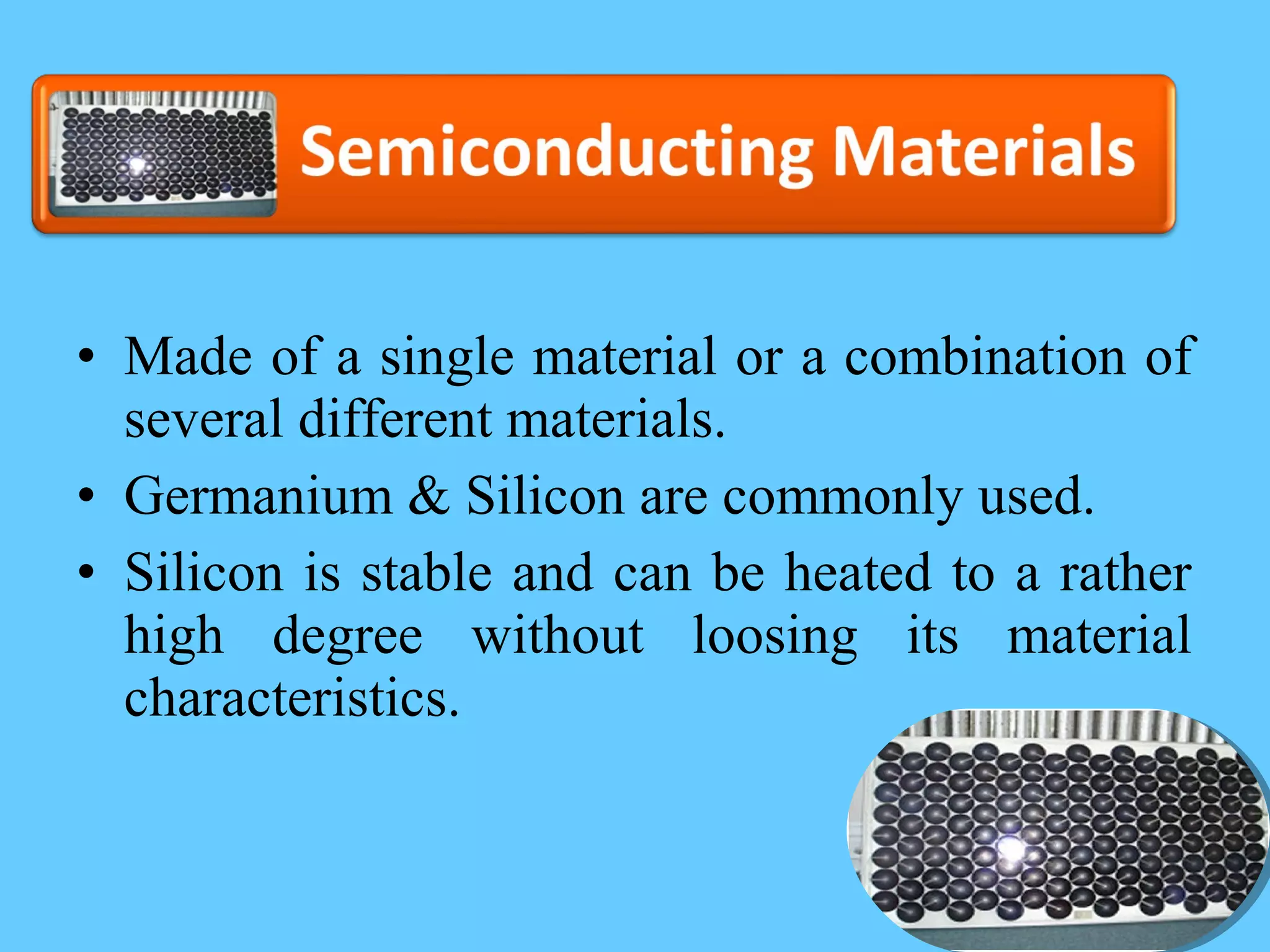
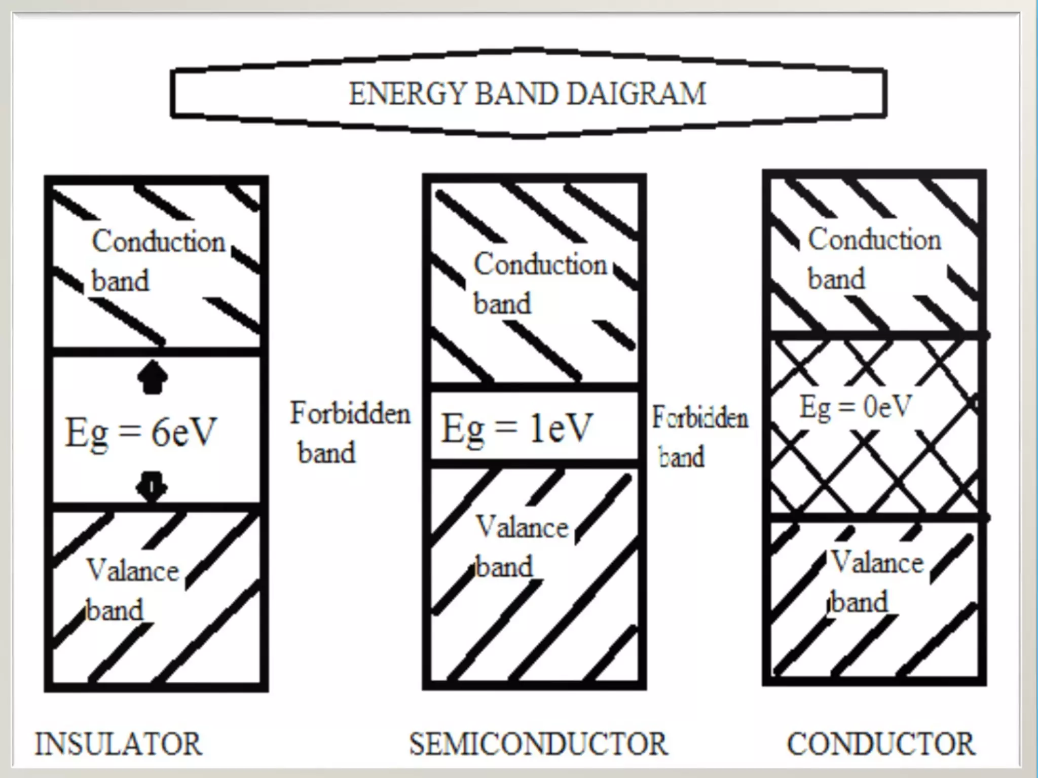
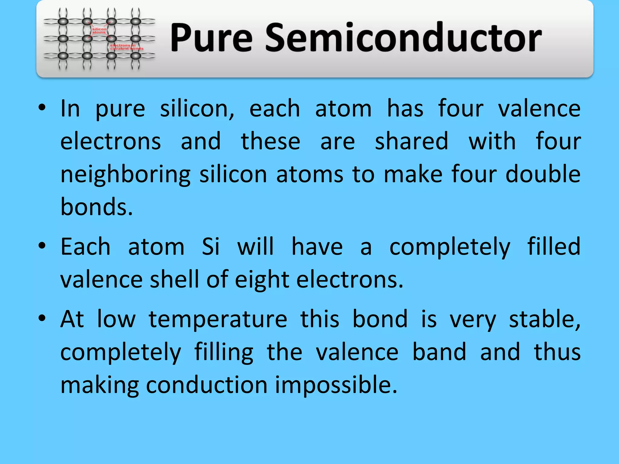
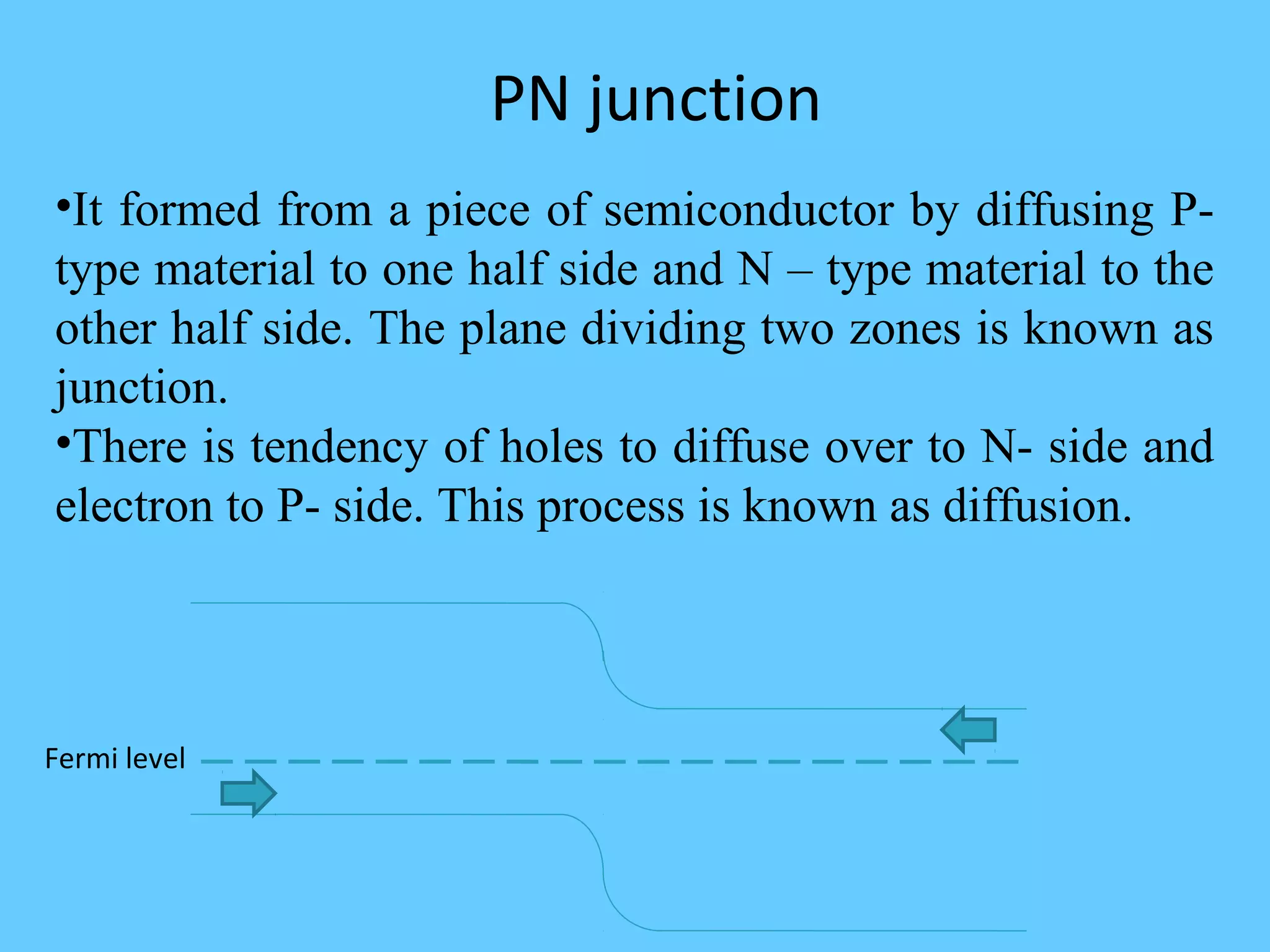
Solar energy can be directly converted into electrical energy.
Energy conversion devices which are used to convert sunlight into electricity by the use of photovoltaic effect are called solar cell.
SEMICONDUCTORS,BAND THEORY OF SOLIDS,FERMI-DIRAC PROBABILITY,DISTRIBUTION FUN...A K Mishra
This PPT contains valence band,conduction band& forbidden energy gap,Free carrier charge density,intrinsic and extrinsic semiconductors,Conductivity in semiconductors
SEMICONDUCTORS,BAND THEORY OF SOLIDS,FERMI-DIRAC PROBABILITY,DISTRIBUTION FUN...A K Mishra
This PPT contains valence band,conduction band& forbidden energy gap,Free carrier charge density,intrinsic and extrinsic semiconductors,Conductivity in semiconductors
Environmental Pollution can be defined as any undesirable change in physical, chemical, or biological characteristics of any component of the environment i.e. air, water, soil which can cause harmful effects on various forms of life or property.
Thermoelectric power generation (TEG) devices typically use special semiconductor materials, which are optimized for the Seebeck effect. The simplest TEG device consists of a thermocouple, comprising a p-type and n-type material connected electrically in series and thermally in parallel.
Heat is applied into one side of the couple and rejected from the opposite side. An electrical current is produced, proportional to the temperature gradient between the hot and cold junctions.
2024.06.01 Introducing a competency framework for languag learning materials ...Sandy Millin
http://sandymillin.wordpress.com/iateflwebinar2024
Published classroom materials form the basis of syllabuses, drive teacher professional development, and have a potentially huge influence on learners, teachers and education systems. All teachers also create their own materials, whether a few sentences on a blackboard, a highly-structured fully-realised online course, or anything in between. Despite this, the knowledge and skills needed to create effective language learning materials are rarely part of teacher training, and are mostly learnt by trial and error.
Knowledge and skills frameworks, generally called competency frameworks, for ELT teachers, trainers and managers have existed for a few years now. However, until I created one for my MA dissertation, there wasn’t one drawing together what we need to know and do to be able to effectively produce language learning materials.
This webinar will introduce you to my framework, highlighting the key competencies I identified from my research. It will also show how anybody involved in language teaching (any language, not just English!), teacher training, managing schools or developing language learning materials can benefit from using the framework.
Operation “Blue Star” is the only event in the history of Independent India where the state went into war with its own people. Even after about 40 years it is not clear if it was culmination of states anger over people of the region, a political game of power or start of dictatorial chapter in the democratic setup.
The people of Punjab felt alienated from main stream due to denial of their just demands during a long democratic struggle since independence. As it happen all over the word, it led to militant struggle with great loss of lives of military, police and civilian personnel. Killing of Indira Gandhi and massacre of innocent Sikhs in Delhi and other India cities was also associated with this movement.
We all have good and bad thoughts from time to time and situation to situation. We are bombarded daily with spiraling thoughts(both negative and positive) creating all-consuming feel , making us difficult to manage with associated suffering. Good thoughts are like our Mob Signal (Positive thought) amidst noise(negative thought) in the atmosphere. Negative thoughts like noise outweigh positive thoughts. These thoughts often create unwanted confusion, trouble, stress and frustration in our mind as well as chaos in our physical world. Negative thoughts are also known as “distorted thinking”.
How to Split Bills in the Odoo 17 POS ModuleCeline George
Bills have a main role in point of sale procedure. It will help to track sales, handling payments and giving receipts to customers. Bill splitting also has an important role in POS. For example, If some friends come together for dinner and if they want to divide the bill then it is possible by POS bill splitting. This slide will show how to split bills in odoo 17 POS.
This is a presentation by Dada Robert in a Your Skill Boost masterclass organised by the Excellence Foundation for South Sudan (EFSS) on Saturday, the 25th and Sunday, the 26th of May 2024.
He discussed the concept of quality improvement, emphasizing its applicability to various aspects of life, including personal, project, and program improvements. He defined quality as doing the right thing at the right time in the right way to achieve the best possible results and discussed the concept of the "gap" between what we know and what we do, and how this gap represents the areas we need to improve. He explained the scientific approach to quality improvement, which involves systematic performance analysis, testing and learning, and implementing change ideas. He also highlighted the importance of client focus and a team approach to quality improvement.
Students, digital devices and success - Andreas Schleicher - 27 May 2024..pptxEduSkills OECD
Andreas Schleicher presents at the OECD webinar ‘Digital devices in schools: detrimental distraction or secret to success?’ on 27 May 2024. The presentation was based on findings from PISA 2022 results and the webinar helped launch the PISA in Focus ‘Managing screen time: How to protect and equip students against distraction’ https://www.oecd-ilibrary.org/education/managing-screen-time_7c225af4-en and the OECD Education Policy Perspective ‘Students, digital devices and success’ can be found here - https://oe.cd/il/5yV
Unit 8 - Information and Communication Technology (Paper I).pdfThiyagu K
This slides describes the basic concepts of ICT, basics of Email, Emerging Technology and Digital Initiatives in Education. This presentations aligns with the UGC Paper I syllabus.
The Indian economy is classified into different sectors to simplify the analysis and understanding of economic activities. For Class 10, it's essential to grasp the sectors of the Indian economy, understand their characteristics, and recognize their importance. This guide will provide detailed notes on the Sectors of the Indian Economy Class 10, using specific long-tail keywords to enhance comprehension.
For more information, visit-www.vavaclasses.com
Synthetic Fiber Construction in lab .pptxPavel ( NSTU)
Synthetic fiber production is a fascinating and complex field that blends chemistry, engineering, and environmental science. By understanding these aspects, students can gain a comprehensive view of synthetic fiber production, its impact on society and the environment, and the potential for future innovations. Synthetic fibers play a crucial role in modern society, impacting various aspects of daily life, industry, and the environment. ynthetic fibers are integral to modern life, offering a range of benefits from cost-effectiveness and versatility to innovative applications and performance characteristics. While they pose environmental challenges, ongoing research and development aim to create more sustainable and eco-friendly alternatives. Understanding the importance of synthetic fibers helps in appreciating their role in the economy, industry, and daily life, while also emphasizing the need for sustainable practices and innovation.
The Roman Empire A Historical Colossus.pdfkaushalkr1407
The Roman Empire, a vast and enduring power, stands as one of history's most remarkable civilizations, leaving an indelible imprint on the world. It emerged from the Roman Republic, transitioning into an imperial powerhouse under the leadership of Augustus Caesar in 27 BCE. This transformation marked the beginning of an era defined by unprecedented territorial expansion, architectural marvels, and profound cultural influence.
The empire's roots lie in the city of Rome, founded, according to legend, by Romulus in 753 BCE. Over centuries, Rome evolved from a small settlement to a formidable republic, characterized by a complex political system with elected officials and checks on power. However, internal strife, class conflicts, and military ambitions paved the way for the end of the Republic. Julius Caesar’s dictatorship and subsequent assassination in 44 BCE created a power vacuum, leading to a civil war. Octavian, later Augustus, emerged victorious, heralding the Roman Empire’s birth.
Under Augustus, the empire experienced the Pax Romana, a 200-year period of relative peace and stability. Augustus reformed the military, established efficient administrative systems, and initiated grand construction projects. The empire's borders expanded, encompassing territories from Britain to Egypt and from Spain to the Euphrates. Roman legions, renowned for their discipline and engineering prowess, secured and maintained these vast territories, building roads, fortifications, and cities that facilitated control and integration.
The Roman Empire’s society was hierarchical, with a rigid class system. At the top were the patricians, wealthy elites who held significant political power. Below them were the plebeians, free citizens with limited political influence, and the vast numbers of slaves who formed the backbone of the economy. The family unit was central, governed by the paterfamilias, the male head who held absolute authority.
Culturally, the Romans were eclectic, absorbing and adapting elements from the civilizations they encountered, particularly the Greeks. Roman art, literature, and philosophy reflected this synthesis, creating a rich cultural tapestry. Latin, the Roman language, became the lingua franca of the Western world, influencing numerous modern languages.
Roman architecture and engineering achievements were monumental. They perfected the arch, vault, and dome, constructing enduring structures like the Colosseum, Pantheon, and aqueducts. These engineering marvels not only showcased Roman ingenuity but also served practical purposes, from public entertainment to water supply.
1. Delivered byDelivered by
Miss. Madhuri MoreMiss. Madhuri More
DEPARTMENT OF RENEWABLE ENERGY
ENGINERRING.
CTAE, MPUAT, Udaipur.
BASICS OFBASICS OF
SEMICONDUCTORSEMICONDUCTOR
2.
3.
4.
5.
6. • We can very easily control how current passes
through them.
• Metal conducts electricity under almost any
condition.
7. • Made of a single material or a combination of
several different materials.
• Germanium & Silicon are commonly used.
• Silicon is stable and can be heated to a rather
high degree without loosing its material
characteristics.
8.
9. • In an atom the number of protons is always
equal to the number of electrons.
10. • Highest energy band that is occupied by
electrons in a material is called the valence
band
• The band with energy one step higher than the
valence band is the conduction band.
• The energy gap between these two bands,
where no electrons are allowed, is called the
band gap.
13. • To get a semiconductor to conduct a current, we
must make an electron jump from an occupied to
an unoccupied energy level.
• When it does this it leaves a hole (an empty
state), This hole can be filled by another electron,
which itself leaves a new hole.
• Both the hole and the electron contribute to the
conductivity as they move around in the material.
15. • The process of adding impurity to a
semiconductor is know as doping.
• By doping, we increase its ability to conduct a
current.
• Two forms of doping, p and n. p stands for
positive and n for negative
• Intrinsic semiconductor
• Extrinsic semiconductors
16. • In pure silicon, each atom has four valence
electrons and these are shared with four
neighboring silicon atoms to make four double
bonds.
• Each atom Si will have a completely filled
valence shell of eight electrons.
• At low temperature this bond is very stable,
completely filling the valence band and thus
making conduction impossible.
18. p-Doping p-Doping
• When you add atoms with trivalent atom
to the semiconductor.
• Trivalent atom is known as acceptor
atom.
• In a p-type semiconductor the major
carrier of current are the holes.
20. n-Doping n-Doping
• When you add atoms with pentavalent
atom to the pure semiconducting
material.
• Pentavalent atom is known as donor
atom.
• In the n-type semiconductor the major
carrier of current is the negative
electrons.
22. Conduction band
Valence band
Fermi level
P Type semiconductor
N Type semiconductor
P-type and N-type semiconductor
Fermi level is the energy at
which the probability of a
state being filled by an
electron is exactly one half
23. PN junction
Fermi level
•It formed from a piece of semiconductor by diffusing P-
type material to one half side and N – type material to the
other half side. The plane dividing two zones is known as
junction.
•There is tendency of holes to diffuse over to N- side and
electron to P- side. This process is known as diffusion.
Solar energy can be directly converted into electrical energy.
Energy conversion devices which are used to convert sunlight into electricity by the use of photovoltaic effect are called solar cell.
Solar photovoltaics (SPV) is the process of converting solar radiation
(sunlight) into electricity using a device called solar cell. A solar cell is
a semi-conducting device made of silicon or other materials, which,
when exposed to sunlight, generates electricity. The magnitude of the
electric current generated depends on the intensity of the solar radiation,
exposed area of the solar cell, the type of material used in fabricating
the solar cell, and ambient temperature. Solar cells are connected in
series and parallel combinations to form modules that provide the
required power.
Photovoltaics (often abbreviated as PV) is a simple and elegant method of harnessing the sun's energy. PV devices (solar cells) are unique in that they directly convert the incident solar radiation into electricity, with no noise, pollution or moving parts, making them robust, reliable and long lasting. Solar cells are based on the same principles and materials behind the communications and computer revolutions, and this CDROM covers the operation, use and applications of photovoltaic devices and systems.
We can very easily control how current passes through them.
We don't have that option with metal since metal conducts electricity under almost any condition.
Because of this, semiconductors are ideal for the construction of electric components such as photovoltaic.
The atom consists of three major, extremely small, building blocks called protons, neutrons and electrons.
Protons have a positive charge, while electrons are negatively charged and neutrons are neutral (no charge).
The protons and the neutrons make up the center (nucleus) of the atom, and the electrons orbit around this center.
Since the positive charge is equal to the negative, the single atom appears to be neutral.
The lower energy level of a semiconductor is called the "valence band" (EV) and the energy level at which an electron can be considered free is called the "conduction band“
The band gap is the minimum amount of energy required for an electron to break free of its bound state.
The band gap determines how much energy is needed from the sun for conduction, as well as how much energy is generated.
Free electron and hole produce by thermal energy is called as minority current carrior
We have conduction band and valence band,
Narmally at 00c All electron valence electron in valence band when they get sufficient energy then electron move to the conduction band, when move to conduction band it is free to conduct, basically it is same breaking a bound and this gap is called as band gap it is nothing but energy required to break a bound
In insulator band gap is very large it means more energy required to break a bound. So, few a bound are breaking and few electron are conduct, where is in a conduction band gap is very small or conduction and valence band are over lap each other then large electron are conduct.
In between these semiconductor in which band gap is not a very large nor very small in between these band gap about 1eV or in between 1-2eV
Trivalent atom is known as acceptor atom, because they accept electrons from the surrounding atoms.
Pentavalent atom is known as donor atom, because they donate electrons to the semiconductor.
PV is the Direct conversion of solar energy to electrical energy with out going to intermediate stage of thermal energy and then to electrical energy.
It works on principal of PN junction
If you have P type semiconductor or N type semi conductor, as you now we can identify a band gap between the conduction band and valence band
One band for conduction and another for valance and band gap for si about 1.107ev
Electron when they are in conduction band they are conducting and holes are in valence band they also conducting and average energy of the electron would be given by the level called fermi level. A fermi level between these two and in case P type semi conductor fermi level is closed to valence band and in case of N type semi conductor fermi level is closed to conduction band
When a P- type material is intimately joined to N-type, a P-N junction is formed.
When you join P and N type material then it produce a PN junction, in which fermi level became equal as result band is bend
In this side p type sc and another side n type semi conductor and so there is a band bend
Actually this is the basic theory of PN junction because of band bending electron find it go up of the field and holes find it go down the field, electron flow this way and holes flow this way so they act as diode.
In case of PV cell we use this property but addition to that what is not in the normal diode is, that light is falling to a very close to the band bending resign, as result light incident upon the material electron will absorb the photon and if photon energy bigger then band gap energy then electron hole pair is created(Electron going to the conduction band and naturally hole goes to the valance band)
Now imagine electron hole pair created just imagine one E H pair created, then if the light has energy bigger then band gap energy
Naturally electron natural tendency flow down and some what electron created hear holes flow up and holes created hear, as a result holes concentrated left side and electron concentrate at right side
If you put a charge collector both side and connect by resistance then charge flow continually, current direction is this way
If you put a charge collector both side and connect by resistance then charge flow continually, current flow direction is this way ,
in which creation of electron hole pair close to the bending resign, it means that large area exposed to sun light and hole pn is over that area