Downloaded 2,895 times

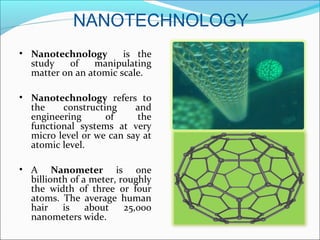
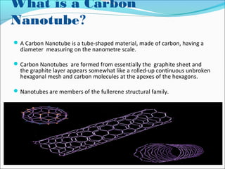
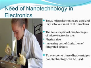
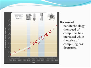
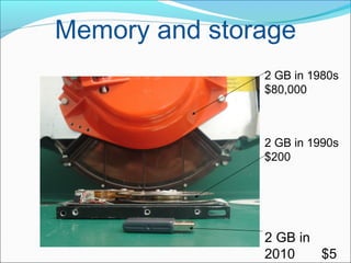
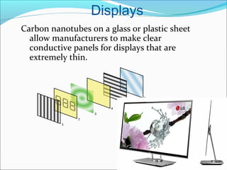
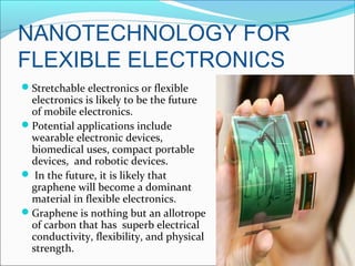
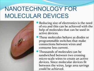


The document discusses nanotechnology, defined as manipulating matter at the atomic scale, emphasizing its significance in electronics. It highlights the advantages of using nanotechnology, such as increasing the density of circuits and improving the efficiency of devices like transistors and sensors. Future prospects include developments in flexible electronics and molecular devices, leveraging materials like graphene to revolutionize electronic applications.


