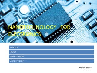
Nanotechnology involves working at the nanoscale (10-100nm) to create new materials with unique properties. It can make electronics smaller, faster, more sensitive and efficient. Carbon nanomaterials like graphene and nanotubes have excellent electrical and mechanical properties making them useful for new types of transistors, sensors and memory. Molecular electronics uses single molecules as building blocks. Quantum computing and spintronics also exploit quantum effects at the nanoscale. Applications include faster computers, larger data storage, improved displays, medical devices and renewable energy.
This PPT is about Nano-Biotechnology and its applications.
This presentation Secured 2nd Prize in State level competition on the Topic of EMERGING TECHNOLOGY IN COMPUTER SCIENCE conducted at S.V.D. Government Degree College for Women, Nidadavolu.
This Small PowerPoint Presentation is given by P.Nikhil, D.Dhanunjaya Rao from Government College, Rajahmundry.
Hope it is useful for future Generation.
Thank You.
Introduction
Definition
History
Advantages of nanobiotechnology
Applications of nanobiotechnology
Drawback of nanobiotechnology
New features in the nanobiotechnology
Conclusion
References
History.
Definition.
Techniques of nanotechnology.
Application in nanotechnology.(Nanomedicine,)
(Nanoelectronics,Nanoagriculture,Nanospace and many others)
Advantages of nanotechnology.
Disadvantages of nanotechnology.
Conclusion.
The Next Very BIG (small) Thing
Contents:
Introduction to Nanotechnology
Applications In Today's Life
Advantages & Disadvantages
Future Of Nanotechnoogy
Nanotechnology is combination of words nano and technology which means very small size of technology. As we all see, day-by-day the size of the objects shrink, so that they can be easily transportable, easily handle. so nanotechnology helps a lot in this digital world.
Evolution of nanotechnology in electronics (seminar report) -codewithgauriGaurav Pandey
Nanotechnology is engineering and manufacturing at the molecular scale, thereby taking more advantage of the unique properties that exist at that scale.
A Nanometre is a unit of length in the metric system, equal to one billionth of a metre(10-9).Can be used across all the other science fields, such as chemistry, biology, physics, materials science, and engineering.
www.blog.codewithgauri.tech
It is an unforgettable thing and it is the first conference paper which I have presented in my university. This describes how the Nanotechnology alters the world to advance. It also has lots of applications due to it's large surface area.
Nanotechnology presentation present by Fares M. AL Makrahy at Department of Pesticides Chemistry &Toxicology, Faculty of Agriculture, Alexandria University During presentations in the department for postgraduate students
Enginneered nanoparticles and microbial activity- Dinesh et al (2012)Raghavan Dinesh
This presentation is based on our review paper ‘Engineered nanoparticles in the soil and their potential implications to microbial activity’, Geoderma, 2012, 173-174, 19-27 (http://dx.doi.org/10.1016/j.geoderma.2011.12.018)
INDIA'S FIRST MARS SPACE MISSION NAMED MARS ORBITER MISSION(MOM) SIMPLY KNOWN AS MANGALYAN. FOR MORE UPDATES AND SLIDES VISIT www.mechanizeinn.wordpress.com OR www.facebook.com/mechanizeinn
Mars orbiter mission (Mangalyaan)The govt. of INDIAArchit Jindal
All details of the Mars orbiter mission of India. Also the details about ISRO who is carrying out this mission. Also Mp4 video of launch of PSLV-XL which was the launch vehicle for the spacecraft. I hope this presentation is useful for you.The video will work.
the branch of technology that deals with dimensions and tolerances of less than 100 nanometres, especially the manipulation of individual atoms and molecules.
Acetabularia Information For Class 9 .docxvaibhavrinwa19
Acetabularia acetabulum is a single-celled green alga that in its vegetative state is morphologically differentiated into a basal rhizoid and an axially elongated stalk, which bears whorls of branching hairs. The single diploid nucleus resides in the rhizoid.
Introduction to AI for Nonprofits with Tapp NetworkTechSoup
Dive into the world of AI! Experts Jon Hill and Tareq Monaur will guide you through AI's role in enhancing nonprofit websites and basic marketing strategies, making it easy to understand and apply.
Macroeconomics- Movie Location
This will be used as part of your Personal Professional Portfolio once graded.
Objective:
Prepare a presentation or a paper using research, basic comparative analysis, data organization and application of economic information. You will make an informed assessment of an economic climate outside of the United States to accomplish an entertainment industry objective.
Instructions for Submissions thorugh G- Classroom.pptxJheel Barad
This presentation provides a briefing on how to upload submissions and documents in Google Classroom. It was prepared as part of an orientation for new Sainik School in-service teacher trainees. As a training officer, my goal is to ensure that you are comfortable and proficient with this essential tool for managing assignments and fostering student engagement.
How to Make a Field invisible in Odoo 17Celine George
It is possible to hide or invisible some fields in odoo. Commonly using “invisible” attribute in the field definition to invisible the fields. This slide will show how to make a field invisible in odoo 17.
The French Revolution, which began in 1789, was a period of radical social and political upheaval in France. It marked the decline of absolute monarchies, the rise of secular and democratic republics, and the eventual rise of Napoleon Bonaparte. This revolutionary period is crucial in understanding the transition from feudalism to modernity in Europe.
For more information, visit-www.vavaclasses.com
Welcome to TechSoup New Member Orientation and Q&A (May 2024).pdfTechSoup
In this webinar you will learn how your organization can access TechSoup's wide variety of product discount and donation programs. From hardware to software, we'll give you a tour of the tools available to help your nonprofit with productivity, collaboration, financial management, donor tracking, security, and more.
Francesca Gottschalk - How can education support child empowerment.pptxEduSkills OECD
Francesca Gottschalk from the OECD’s Centre for Educational Research and Innovation presents at the Ask an Expert Webinar: How can education support child empowerment?
Embracing GenAI - A Strategic ImperativePeter Windle
Artificial Intelligence (AI) technologies such as Generative AI, Image Generators and Large Language Models have had a dramatic impact on teaching, learning and assessment over the past 18 months. The most immediate threat AI posed was to Academic Integrity with Higher Education Institutes (HEIs) focusing their efforts on combating the use of GenAI in assessment. Guidelines were developed for staff and students, policies put in place too. Innovative educators have forged paths in the use of Generative AI for teaching, learning and assessments leading to pockets of transformation springing up across HEIs, often with little or no top-down guidance, support or direction.
This Gasta posits a strategic approach to integrating AI into HEIs to prepare staff, students and the curriculum for an evolving world and workplace. We will highlight the advantages of working with these technologies beyond the realm of teaching, learning and assessment by considering prompt engineering skills, industry impact, curriculum changes, and the need for staff upskilling. In contrast, not engaging strategically with Generative AI poses risks, including falling behind peers, missed opportunities and failing to ensure our graduates remain employable. The rapid evolution of AI technologies necessitates a proactive and strategic approach if we are to remain relevant.
2. WHAT IS NANOTECHNOLOGY ?
Nanotechnology broadly includes all
technologies that handle nano-scale
materials, and in a narrow sense,
technologies that handle unique
phenomena that arise in the 10-to-100-nm
size range.
Carbon
Nanofibre
(a single
human
hairis 1000
times
thicker
than any of
the
nanofibres
in the
image).
3.
4. NEW PROPERTIES
At the nanoscale, matter begins to
demonstrate entirely new and unique
properties. It can become stronger,
conduct heat better, and show
extraordinary electrical properties.
8. WHY NANOTECHNOLOGY MATTERS ?
• The advances in nanotechnology have brought new
tools to the field of electronics and sensors.
• For instance, at the nanoscale, the resistance
dependence of a material on an external magnetic
field is significantly amplified, which has led to the
fabrication of hard disks with a data storage density
in the gigabyte and terabyte ranges.
10. CARBON BASED SENSORS AND ELECTRONICS
Carbon nanomaterials such as one-
dimensional (1D) carbon nanotubes and
two-dimensional (2D) graphene have:-
• Superior electrical properties which allow
for fabrication of faster and more power-
efficient electronics.
• High surface to volume ratio.
• Excellent mechanical properties rendering
them as a robust and highly sensitive
building block for nanosensors.
11. •Graphene transistor
• Graphene is a single sheet of carbon atoms packed in a
honeycomb crystal lattice, isolated from graphite.
• Allows electrons to move at an extraordinarily high speed.
• With its intrinsic nature of being one-atom-thick, can be
exploited to fabricate field-effect transistors that are faster
and smaller.
12. • Carbon nanotube electronics
When a layer of graphene is
rolled into a tube, a single-
walled carbon nanotube
(SWNT) is formed. The
cylindrical structure and
high electron mobility makes
them a more readily
available option for forming
the channel in field-effect
transistors. These have
advanced to logic gates and
radio-frequency
components.
13. • Carbon-based nanosensors
• Graphene and carbon nanotubes have excellent thermal
conductivity, high mechanical robustness, and very large
surface to volume ratio making them superior materials
for fabrication of electromechanical and
electrochemical sensors with higher sensitivities, lower
limits of detection, and faster response time.
Any additional gold atom that adsorbs
on the surface of a vibrating carbon
nanotube would change its resonance
frequency which is further detected.
14. MOLECULAR ELECTRONICS
• Recent advances in nanofabrication
techniques have provided the opportunity to
use single molecules, or a tiny assembly of
them, as the main building blocks of an
electronic circuit.
• Enabling the realisation of novel
functionalities beyond the scope of traditional
solid state devices.
15. • Single Molecule Memory Device
A modern memory device, stores each bit of data by charging
up a tiny capacitor. As memory device dimensions approach
the nanometer range, the capacitor can be replaced by a
single organic molecule such as Ferrocene, whose oxidation
state can be altered by moving an electron into or out of
the molecule.
16. • Organic transistor odour sensor
In an odour sensor, for instance, the nano-scale
chemical reactions upon exposure of the device
to a certain atmospheric condition modify the
electronic properties of the organic
semiconducting material which is further
reflected by a change in the current flowing
through the transistor.
17. QUANTUM COMPUTING
Quantum algorithms are implemented in a
device that makes direct use of quantum
mechanical phenomena such as
entanglement and superposition.
Nanotechnology uses the fact that the
physical laws that govern the behaviour of
a system at the atomic scale are
inherently quantum mechanical in nature.
18. SINGLE ELECTRON TRANSISTOR
• A single electron transistor
needs only one electron to
change from the insulating
to the conducting state.
• Deliver very high device
density and power
efficiency with remarkable
operational speed.
• Quantum dots with sub-100
nm dimensions have to be
fabricated.
19. SPINTRONICS
Spintronics employs the spin of electrons to
encode and transfer information. It has the
potential to deliver nanoscale memory and
logic devices which process information
faster, consume less power, and store more
data in less space. The extension of the hard
disk capacities to the gigabyte and the
terabyte ranges was the main achievement
of spintronics by taking advantage of Giant
Magneto-Resistance (GMR) and Tunnel
Magneto-Resistance (TMR) effects which are
effective only at the nano scale.
20. NANO-ELECTRO-MECHANICAL
SYSTEMS (NEMS)
• Nano-electro-mechanical systems have
evolved during the last 10 years by creating
sensors (“eyes”) and actuators (“arms”).
• Recent developments in synthesis of
nanomaterials with excellent electrical and
mechanical properties have extended the
boundaries of NEMS applications to include
more advanced devices such as the non-
volatile nanoelectro-mechanical memory,
where information is transferred and stored
through a series of electrical and mechanical
actions at the nanoscale.
21.
22. Hybrid Si NanoCones/Polymer
Solar Cell• Si nanocones
fabricated by
colloidal lithography
were covered with a
conductive polymer,
which formed a
Schottky junction
between the Si and
polymer.
• The power
conversion
efficiency of the
hybrid Si/polymer
device was more
than 11 %.
24. • Computer processing
Moore’s Law
describes a
trend of
technology. It
states that the
number of
transistors that
can be put on a
single chip will
double every
two years.
26. • Memory and storage
2 GB in 1980s
$80,000
2 GB in 1990s
$200
2 GB in 2010
$5
27. • Displays
Carbon nanotubes on a glass or plastic sheet allow
manufacturers to make clear conductive panels
for displays that are extremely thin.
28. Restoring Sight to the Blind
• Blindness due to loss of photoreceptors.
• Sight can be restored by patterned electrical
stimulation of the surviving inner retinal
neurons.
• Photovoltaic subretinal prosthesis directly
converts pulsed light into pulsed electric current
in each pixel, stimulating nearby neurons.
• Visual information is projected onto retina by
video goggles using pulsed NIR (~900 nm) light.
Photovoltaic arrays including 3 diodes in each
pixels were fabricated in SNF.
29.
30. Cancer Detection
• Motivation – Earlier
cancer detection
• Development of
nanomagnetic
sensor chip
– Use same principles
employed in
magnetic storage
industry
– Use magnetic
nanoparticles to
‘tag’ proteins
indicative of cancer
31. Nanostructures in Nature
• A moth’s eye has very small bumps on its surface. These patterns
are smaller than the wavelength of visible light (350-800nm). The
eye surface has a very low reflectance for the visible light. The
moth can see much better than humans in dim or dark conditions
because these nanostructures absorb light very efficiently.
• On the surface of a butterfly’s wings are multilayer nanoscale
patterns. These structures filter light and reflect mostly one
wavelength, so we see a single bright color. Due to multiple layers
in these structures optical interferences are created (wings of male
Morpho Rhetenor appear blue).
• The edelweiss (Leontopodium nivale) is an alpine flower found at
high altitudes, where UV radiation is strong. The flowers are
covered with thin hollow filaments that have nanoscale structures
(100-200nm) on their periphery. They will absorb ultraviolet light,
but reflect all visible light. This explains the white color of the
flower. It also protects the flower’s cells from possible damage due
to this high-energy radiation.
32.
33. • Providing realistic, cost-effective methods
for harnessing renewable energy sources
and keeping the environment clean.
• Doctors detecting disease at its earliest
stages and treating illnesses such as cancer,
diabetes, heart disease with more effective
and safer medicines.
• New technologies for protecting both
military forces and civilians from
conventional, chemical and biological
weapons.