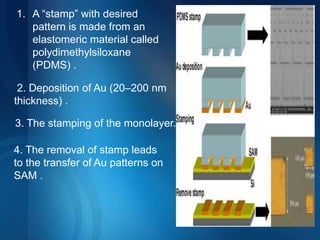
Nano Electronics


By
Bharanidharan G
Jesuraj J
Introduction
Basics of SAMs
Characterization of SAMs
Lithography
Conduction in SAMs
SAM Devices
Conclusion
Current trends in nanoelectronics

The development of new applications.

 The miniaturization of existing ones.

This gives the idea to emerge a new field

Molecular Electronics fulfill the need.
Introduction
Basics of SAMs
Characterization of SAMs
Lithography
Conduction in SAMs
SAM Devices
Conclusion
A self assembled monolayer (SAM) is an
organized layer of amphiphilic molecules .

The interesting fact is
these layers are water
loving and fat loving.

This property of SAM
makes it to be
implemented in medical
field.
They assemble themselves on a substrate
namely silicon.

They have three parts ,they are head group ,
alkyl chain ,surface group.

 Head group gets adsorbed
on substrate.

 Alkyl chain links head
group and the surface group.

Surface group forms a layer to attach metal
group.
Introduction
Basics of SAMs
Characterization of SAMs
Lithography
Conduction in SAMs
SAM Devices
Conclusion
Processes of the SAM formation on a native silicon oxide
surface of Si is followed by thorough rinsing in DI water then
drying under nitrogen.
Introduction
Basics of SAMs
Characterization of SAMs
Lithography
Conduction in SAMs
SAM Devices
Conclusion
1. A “stamp” with desired
   pattern is made from an
   elastomeric material called
   polydimethylsiloxane
   (PDMS) .

 2. Deposition of Au (20–200 nm
thickness) .

3. The stamping of the monolayer.

4. The removal of stamp leads
to the transfer of Au patterns on
SAM .
Introduction
Basics of SAMs
Characterization of SAMs
Lithography
Conduction in SAMs
SAM Devices
Conclusion
Electronic conduction in SAMs
Conduction takes place between HOMO and
LOMO layer.

Conductions are mainly due to Tunneling effect.
Introduction
Basics of SAMs
Characterization of SAMs
Lithography
Conduction in SAMs
SAM Devices
Conclusion
Molecular rectifier


Molecular transistor
Advantages
The size is few nano meters so consequently the size of device
reduces.

No waste of energy due to heat dissipation .

Thus efficiency of the system increases and the operation is
precise.
Disadvantages
The lithography technique is minute
in nano scale so difficult to
manufacture.

Should be handled carefully.
Nanoelectronics

Nanoelectronics