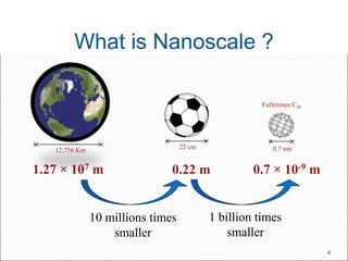
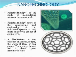
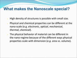
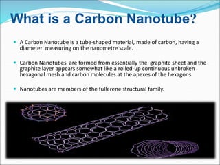
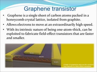
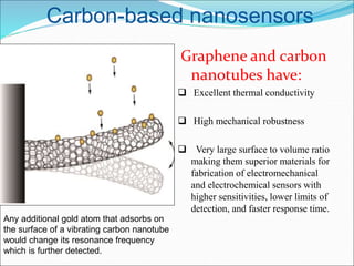
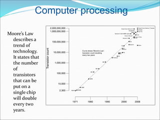
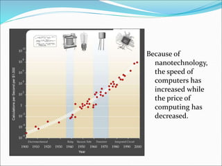
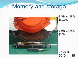
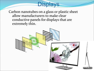
DEPARTMENT OF ELECTRONICS & COMMUNICATION ENGINEERING
Technical Seminar Presentation
On
NANO-TECHNMOLOGY
IN
ELECTRONIOC DEVICES
”
Presented By:
Name: Afroz Ali
1VI20EC002
VIII Sem ‘A’ Section
Department of ECE,
Vemana IT
Guided By:
Name: XXX
Designation: XXX
Department of ECE, Vemana IT
CONTENTS
 Introduction
 What is “Nanoscale”?
 Nanotechnology
 What makes the Nanoscale special?
 Need of Nanotechnology in Electronics
 Nanotechnology in Electronics
 Common Applications of Nanotechnology in
Electronics
 Future Scope of Nanotechnology
 References
INTRODUCTION
What is “Nano”?
Nano in Greek means
‘dwarf’…..but in actual Nano is even smaller
than dwarf i.e atomic level of anything.
What is Nanoscale ?
1.27 × 10⁷ m 0.22 m 0.7 × 10⁻⁹ m
Fullerenes C60
12,756 Km 22 cm 0.7 nm
10 millions times
smaller
1 billion times
smaller
4
NANOTECHNOLOGY
• Nanotechnology is the
study of manipulating
matter on an atomic scale.
• Nanotechnology refers to
the constructing and
engineering of the
functional systems at very
micro level or we can say at
atomic level.
• A Nanometer is one
billionth of a meter, roughly
the width of three or four
atoms. The average human
hair is about 25,000
nanometers wide.
What makes the Nanoscale special?
 High density of structures is possible with small size.
 Physical and chemical properties can be different at the
nano-scale (e.g. electronic, optical, mechanical,
thermal, chemical).
 The physical behavior of material can be different in
the nano-regime because of the different ways physical
properties scale with dimension (e.g. area vs. volume).
What is a Carbon Nanotube?
 A Carbon Nanotube is a tube-shaped material, made of carbon, having a
diameter measuring on the nanometre scale.
 Carbon Nanotubes are formed from essentially the graphite sheet and the
graphite layer appears somewhat like a rolled-up continuous unbroken
hexagonal mesh and carbon molecules at the apexes of the hexagons.
 Nanotubes are members of the fullerene structural family.
Need of Nanotechnology in
Electronics
 Today microelectronics are used and
they solve our most of the problems.
 The two exceptional disadvantages of
micro electronics are:
 Physical size
 Increasing cost of fabrication of
integrated circuits.
 To overcome these disadvantages
nanotechnology can be used.
Nanotechnology in Electronics
 Nanoelectronics refer to the use of nanotechnology
on electronic components, especially transistors.
 Nanoelectronics often refer to transistor devices that are so
small that inter-atomic interactions and quantum
mechanical properties need to be studied extensively.
 Besides being small and allowing more transistors to be
packed into a single chip, the uniform and symmetrical
structure of nanotubes allows a higher electron mobility, a
higher dielectric constant (faster frequency), and a
symmetrical electron/ hole characteristic.
 Increasing the density of
memory chips
 Decreasing the weight and
thickness of the screens
 Nanolithography is used for
fabrication of chips.
 Reducing the size of transistors
used in integrated circuits.
 Improving display screens on
electronics devices.
 Reducing power consumption.
Advantages of Using Nanotechnology in
Electronics
Graphene transistor
• Graphene is a single sheet of carbon atoms packed in a
honeycomb crystal lattice, isolated from graphite.
• Allows electrons to move at an extraordinarily high speed.
• With its intrinsic nature of being one-atom-thick, can be
exploited to fabricate field-effect transistors that are faster
and smaller.
Single Electron Transistor
• A single electron
transistor needs only one
electron to change from
the insulating to the
conducting state.
• Deliver very high device
density and power
efficiency with remarkable
operational speed.
• Quantum dots with sub-
100 nm dimensions have to
be fabricated.
Carbon-based nanosensors
Graphene and carbon
nanotubes have:
 Excellent thermal conductivity
 High mechanical robustness
 Very large surface to volume ratio
making them superior materials for
fabrication of electromechanical
and electrochemical sensors with
higher sensitivities, lower limits of
detection, and faster response time.
Any additional gold atom that adsorbs on
the surface of a vibrating carbon nanotube
would change its resonance frequency
which is further detected.
Computer processing
Moore’s Law
describes a
trend of
technology.
It states that
the number
of
transistors
that can be
put on a
single chip
will double
every two
years.
Because of
nanotechnology,
the speed of
computers has
increased while
the price of
computing has
decreased.
Memory and storage
2 GB in 1980s
$80,000
2 GB in 1990s
$200
2 GB in
2010 $5
Displays
Carbon nanotubes on a glass or plastic sheet
allow manufacturers to make clear
conductive panels for displays that are
extremely thin.
FUTURE SCOPE IN
NANOTECHNOLOGY
 Nanotechnology for flexible Electronics
 Nanotechnology for wireless devices
 Nanotechnology for molecular devices
References :
 [1] Xiaolong Luo, Junhua Long, Qiangjian Sun, Zhitao Chen, Xiaoxu Wu, Xufei Li, Menglu Yu, Huyin Zhao, Xiaoming Shen,
Shulong Lu, "Monolithic 24u2009u2009cm2 flexible triple-junction solar cell encapsulated module based on the ipsilateral
electrode welding technology", Applied Optics, vol.63, no.11, pp.2815, 2024.
 [2] Liga Avotina, Liga Bikse, Yuri Dekhtyar, Annija Elizabete Goldmane, Gunta Kizane, Aleksei Muhin, Marina Romanova,
Krisjanis Smits, Hermanis Sorokins, Aleksandr Vilken, Aleksandrs Zaslavskis, "Tungsten–SiO2–Based Planar Field Emission
Microtriodes with Different Electrode Topologies", Materials, vol.16, no.17, pp.5781, 2023.
 [3] Anatoly G. Kolosko, Sergey V. Filippov, Eugeni O. Popov, Sergey A. Ponyaev, Alexandr V. Shchegolkov, "Investigation of
the current level instability of the multitip field emitters with computerized field emission projector", Journal of Vacuum
Science & Technology B, vol.38, no.6, pp.062806, 2020.
 [4] Shruti Nirantar, Taimur Ahmed, Guanghui Ren, Philipp Gutruf, Chenglong Xu, Madhu Bhaskaran, Sumeet Walia, Sharath
Sriram, "Metal–Air Transistors: Semiconductor-Free Field-Emission AirChannel Nanoelectronics", Nano Letters, vol.18,
no.12, pp.7478, 2018.
 [5] Xingwang Shen, Junjie Li, Shuang Xi, "High Strength Die-Attach Joint Formation by Pressureless Sintering of Organic
Amine Modified Ag Nanoparticle Paste", Nanomaterials, vol.12, no.19, pp.3351, 2022.
 [6] Ruihan Huang, Haiquan Zhao, Yazhou Wei, Feiliang Chen, Jian Zhang, Mo Li, "A suspended micro-bridge structure nano-
air-channel triode with a deformable anode", 2023 24th International Vacuum Electronics Conference (IVEC), pp.1-2, 2023.
 [7] Yazhou Wei, Ruihan Huang, Haiquan Zhao, Feiliang Chen, Jian Zhang, Mo Li, "GaN Nanoscale Air-Channel Diodes with
High Rectification Ratio and Irradiation Resistance", 2023 24th International Vacuum Electronics Conference (IVEC), pp.1-2,
2023.
 [8] Linjie Fan, Jinshun Bi, Biyao Zhao, Gangping Yan, Yue Ma, Fazhan Zhao, "Nanoscale Vacuum Channel Hall Sensors",
IEEE Sensors Journal, vol.22, no.24, pp.23806-23811, 2022.
 [9] Minglei Tang, Chicheng Ma, Lining Liu, Xiaolong Tan, Yan Li, Young Jin Lee, Guodong Wang, Dae-Woo Jeon, Ji-Hyeon
Park, Yiyun Zhang, Xiaoyan Yi, Junxi Wang, Jinmin Li, "β-Ga2O3 Air-Channel FieldEmission Nanodiode with Ultrahigh
Current Density and Low Turn-On Voltage", Nano Letters, 2024.
 [10]idan He, Zhiwei Li, Shuyu Mao, Fangyuan Zhan, Xianlong Wei, "A Vacuum Transistor Based on Field-Assisted
Thermionic Emission from a Multiwalled Carbon Nanotube", Electronics, vol.11, no.3, pp.399, 2022
"The Next Big Thing Is Really Small”

he description abouty tech semina,m M< b, M <NBr

  • 1.
    DEPARTMENT OF ELECTRONICS& COMMUNICATION ENGINEERING Technical Seminar Presentation On NANO-TECHNMOLOGY IN ELECTRONIOC DEVICES ” Presented By: Name: Afroz Ali 1VI20EC002 VIII Sem ‘A’ Section Department of ECE, Vemana IT Guided By: Name: XXX Designation: XXX Department of ECE, Vemana IT
  • 2.
    CONTENTS  Introduction  Whatis “Nanoscale”?  Nanotechnology  What makes the Nanoscale special?  Need of Nanotechnology in Electronics  Nanotechnology in Electronics  Common Applications of Nanotechnology in Electronics  Future Scope of Nanotechnology  References
  • 3.
    INTRODUCTION What is “Nano”? Nanoin Greek means ‘dwarf’…..but in actual Nano is even smaller than dwarf i.e atomic level of anything.
  • 4.
    What is Nanoscale? 1.27 × 10⁷ m 0.22 m 0.7 × 10⁻⁹ m Fullerenes C60 12,756 Km 22 cm 0.7 nm 10 millions times smaller 1 billion times smaller 4
  • 5.
    NANOTECHNOLOGY • Nanotechnology isthe study of manipulating matter on an atomic scale. • Nanotechnology refers to the constructing and engineering of the functional systems at very micro level or we can say at atomic level. • A Nanometer is one billionth of a meter, roughly the width of three or four atoms. The average human hair is about 25,000 nanometers wide.
  • 6.
    What makes theNanoscale special?  High density of structures is possible with small size.  Physical and chemical properties can be different at the nano-scale (e.g. electronic, optical, mechanical, thermal, chemical).  The physical behavior of material can be different in the nano-regime because of the different ways physical properties scale with dimension (e.g. area vs. volume).
  • 7.
    What is aCarbon Nanotube?  A Carbon Nanotube is a tube-shaped material, made of carbon, having a diameter measuring on the nanometre scale.  Carbon Nanotubes are formed from essentially the graphite sheet and the graphite layer appears somewhat like a rolled-up continuous unbroken hexagonal mesh and carbon molecules at the apexes of the hexagons.  Nanotubes are members of the fullerene structural family.
  • 8.
    Need of Nanotechnologyin Electronics  Today microelectronics are used and they solve our most of the problems.  The two exceptional disadvantages of micro electronics are:  Physical size  Increasing cost of fabrication of integrated circuits.  To overcome these disadvantages nanotechnology can be used.
  • 9.
    Nanotechnology in Electronics Nanoelectronics refer to the use of nanotechnology on electronic components, especially transistors.  Nanoelectronics often refer to transistor devices that are so small that inter-atomic interactions and quantum mechanical properties need to be studied extensively.  Besides being small and allowing more transistors to be packed into a single chip, the uniform and symmetrical structure of nanotubes allows a higher electron mobility, a higher dielectric constant (faster frequency), and a symmetrical electron/ hole characteristic.
  • 10.
     Increasing thedensity of memory chips  Decreasing the weight and thickness of the screens  Nanolithography is used for fabrication of chips.  Reducing the size of transistors used in integrated circuits.  Improving display screens on electronics devices.  Reducing power consumption. Advantages of Using Nanotechnology in Electronics
  • 12.
    Graphene transistor • Grapheneis a single sheet of carbon atoms packed in a honeycomb crystal lattice, isolated from graphite. • Allows electrons to move at an extraordinarily high speed. • With its intrinsic nature of being one-atom-thick, can be exploited to fabricate field-effect transistors that are faster and smaller.
  • 13.
    Single Electron Transistor •A single electron transistor needs only one electron to change from the insulating to the conducting state. • Deliver very high device density and power efficiency with remarkable operational speed. • Quantum dots with sub- 100 nm dimensions have to be fabricated.
  • 14.
    Carbon-based nanosensors Graphene andcarbon nanotubes have:  Excellent thermal conductivity  High mechanical robustness  Very large surface to volume ratio making them superior materials for fabrication of electromechanical and electrochemical sensors with higher sensitivities, lower limits of detection, and faster response time. Any additional gold atom that adsorbs on the surface of a vibrating carbon nanotube would change its resonance frequency which is further detected.
  • 16.
    Computer processing Moore’s Law describesa trend of technology. It states that the number of transistors that can be put on a single chip will double every two years.
  • 17.
    Because of nanotechnology, the speedof computers has increased while the price of computing has decreased.
  • 18.
    Memory and storage 2GB in 1980s $80,000 2 GB in 1990s $200 2 GB in 2010 $5
  • 19.
    Displays Carbon nanotubes ona glass or plastic sheet allow manufacturers to make clear conductive panels for displays that are extremely thin.
  • 20.
    FUTURE SCOPE IN NANOTECHNOLOGY Nanotechnology for flexible Electronics  Nanotechnology for wireless devices  Nanotechnology for molecular devices
  • 21.
    References :  [1]Xiaolong Luo, Junhua Long, Qiangjian Sun, Zhitao Chen, Xiaoxu Wu, Xufei Li, Menglu Yu, Huyin Zhao, Xiaoming Shen, Shulong Lu, "Monolithic 24u2009u2009cm2 flexible triple-junction solar cell encapsulated module based on the ipsilateral electrode welding technology", Applied Optics, vol.63, no.11, pp.2815, 2024.  [2] Liga Avotina, Liga Bikse, Yuri Dekhtyar, Annija Elizabete Goldmane, Gunta Kizane, Aleksei Muhin, Marina Romanova, Krisjanis Smits, Hermanis Sorokins, Aleksandr Vilken, Aleksandrs Zaslavskis, "Tungsten–SiO2–Based Planar Field Emission Microtriodes with Different Electrode Topologies", Materials, vol.16, no.17, pp.5781, 2023.  [3] Anatoly G. Kolosko, Sergey V. Filippov, Eugeni O. Popov, Sergey A. Ponyaev, Alexandr V. Shchegolkov, "Investigation of the current level instability of the multitip field emitters with computerized field emission projector", Journal of Vacuum Science & Technology B, vol.38, no.6, pp.062806, 2020.  [4] Shruti Nirantar, Taimur Ahmed, Guanghui Ren, Philipp Gutruf, Chenglong Xu, Madhu Bhaskaran, Sumeet Walia, Sharath Sriram, "Metal–Air Transistors: Semiconductor-Free Field-Emission AirChannel Nanoelectronics", Nano Letters, vol.18, no.12, pp.7478, 2018.  [5] Xingwang Shen, Junjie Li, Shuang Xi, "High Strength Die-Attach Joint Formation by Pressureless Sintering of Organic Amine Modified Ag Nanoparticle Paste", Nanomaterials, vol.12, no.19, pp.3351, 2022.  [6] Ruihan Huang, Haiquan Zhao, Yazhou Wei, Feiliang Chen, Jian Zhang, Mo Li, "A suspended micro-bridge structure nano- air-channel triode with a deformable anode", 2023 24th International Vacuum Electronics Conference (IVEC), pp.1-2, 2023.  [7] Yazhou Wei, Ruihan Huang, Haiquan Zhao, Feiliang Chen, Jian Zhang, Mo Li, "GaN Nanoscale Air-Channel Diodes with High Rectification Ratio and Irradiation Resistance", 2023 24th International Vacuum Electronics Conference (IVEC), pp.1-2, 2023.  [8] Linjie Fan, Jinshun Bi, Biyao Zhao, Gangping Yan, Yue Ma, Fazhan Zhao, "Nanoscale Vacuum Channel Hall Sensors", IEEE Sensors Journal, vol.22, no.24, pp.23806-23811, 2022.  [9] Minglei Tang, Chicheng Ma, Lining Liu, Xiaolong Tan, Yan Li, Young Jin Lee, Guodong Wang, Dae-Woo Jeon, Ji-Hyeon Park, Yiyun Zhang, Xiaoyan Yi, Junxi Wang, Jinmin Li, "β-Ga2O3 Air-Channel FieldEmission Nanodiode with Ultrahigh Current Density and Low Turn-On Voltage", Nano Letters, 2024.  [10]idan He, Zhiwei Li, Shuyu Mao, Fangyuan Zhan, Xianlong Wei, "A Vacuum Transistor Based on Field-Assisted Thermionic Emission from a Multiwalled Carbon Nanotube", Electronics, vol.11, no.3, pp.399, 2022
  • 22.
    "The Next BigThing Is Really Small”