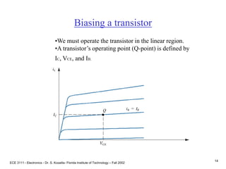
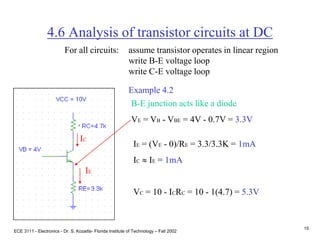
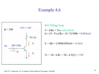
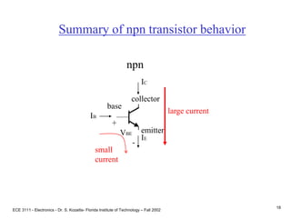
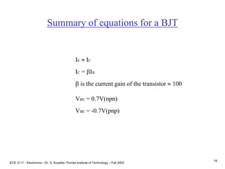
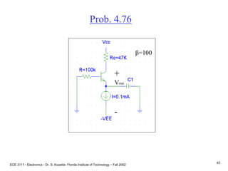
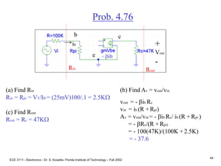
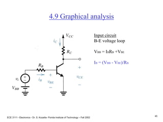
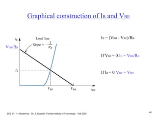
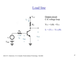
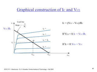
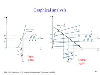
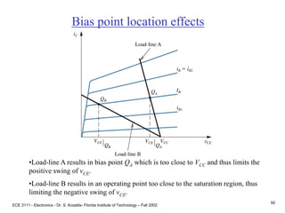
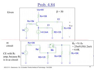
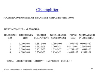
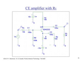
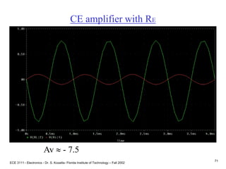
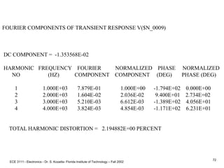
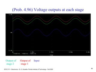
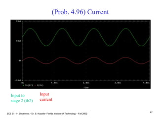
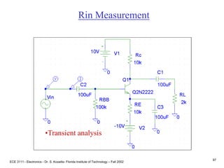
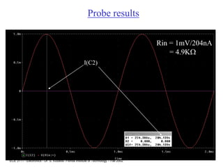
This document contains lecture slides about BJT transistors and amplifier circuits. It discusses BJT biasing, modes of operation, input and output characteristics, and analysis of transistor circuits using voltage loops. Examples are provided to demonstrate analyzing DC operating points and determining AC quantities like transconductance and input resistance. The document also introduces small-signal models for analyzing transistor amplifiers.


![ECE 3111 - Electronics - Dr. S. Kozaitis- Florida Institute of Technology – Fall 2002
20
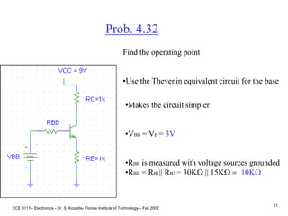
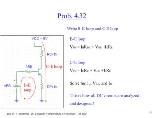
Prob. 4.32
•Use a voltage divider, RB1 and RB2 to bias VB to
avoid two power supplies.
•Make the current in the voltage divider about 10
times IB to simplify the analysis. Use VB = 3V and
I = 0.2mA.
IB
I
(a) RB1 and RB2 form a voltage divider.
Assume I >> IB I = VCC/(RB1 + RB2)
.2mA = 9 /(RB1 + RB2)
AND
VB = VCC[RB2/(RB1 + RB2)]
3 = 9 [RB2/(RB1 + RB2)], Solve for RB1 and RB2.
RB1 = 30KW, and RB2 = 15KW.](https://image.slidesharecdn.com/bjttransistors-converted-190816025303/85/Bjt-transistors-converted-21-320.jpg)
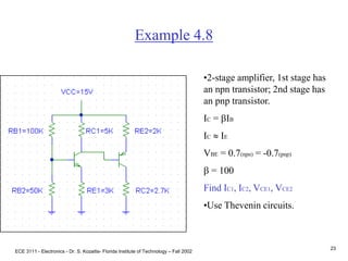
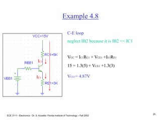
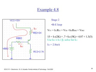
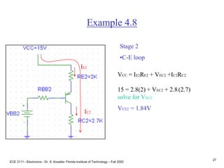
![ECE 3111 - Electronics - Dr. S. Kozaitis- Florida Institute of Technology – Fall 2002
24
Example 4.8
•RBB1 = RB1||RB2 = 33K
•VBB1 = VCC[RB2/(RB1+RB2)]
VBB1 = 15[50K/150K] = 5V
Stage 1
•B-E loop
VBB1 = IB1RBB1 + VBE +IE1RE1
Use IB1 IE1/ b
5 = IE133K/ 100 + .7 + IE13K
IE1 = 1.3mA
IB1
IE1](https://image.slidesharecdn.com/bjttransistors-converted-190816025303/85/Bjt-transistors-converted-25-320.jpg)
![ECE 3111 - Electronics - Dr. S. Kozaitis- Florida Institute of Technology – Fall 2002
31
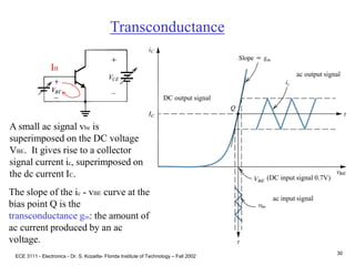
Transconductance = slope at Q point
gm = dic/dvBE|ic = ICQ
where IC = IS[exp(-VBE/VT)-1]; the
equation for a diode.
Transconductance
ac input signal
DC input signal (0.7V)
ac output signal
DC output signal
gm = ISexp(-VBE/VT) (1/VT)
gm IC/VT (A/V)](https://image.slidesharecdn.com/bjttransistors-converted-190816025303/85/Bjt-transistors-converted-32-320.jpg)
![ECE 3111 - Electronics - Dr. S. Kozaitis- Florida Institute of Technology – Fall 2002
36
Example 4.9
ac problem
Short DC sources, input and output circuits are separate, only coupled mathematically
gm = IC/VT = 2.3mA/25mV = 92mA/V
rp = VT/ IB = 25mV/.023mA = 1.1K
vbe= vi [rp / (100K + rp)] = 0.011vi
vout = - gm vbeRC
vout = - 92(0.011vi)3K
vout/vi = -3.04
+
vout
-
e
b c
+
vbe
-](https://image.slidesharecdn.com/bjttransistors-converted-190816025303/85/Bjt-transistors-converted-37-320.jpg)
![ECE 3111 - Electronics - Dr. S. Kozaitis- Florida Institute of Technology – Fall 2002
42
ac equivalent circuit
b
e
c
vbe = (Rb||Rpi)/ [(Rb||Rpi) +Rs]vi
vbe = 0.5vi
vout = -(gmvbe)(Ro||Rc ||RL)
vout = -154vbe
Av =vout/vi = - 77
+
vout
-
Neglecting Ro
vout = -(gmvbe)(Rc ||RL)
Av =vout/vi = - 80](https://image.slidesharecdn.com/bjttransistors-converted-190816025303/85/Bjt-transistors-converted-43-320.jpg)
![ECE 3111 - Electronics - Dr. S. Kozaitis- Florida Institute of Technology – Fall 2002
65
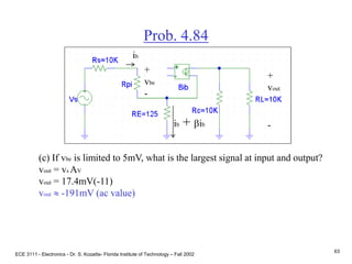
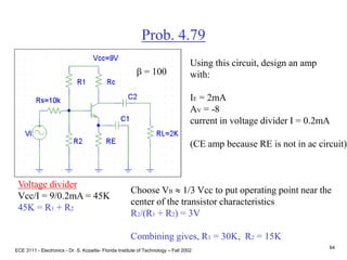
Prob. 4.79
b = 100Find RE (input circuit)
Use Thevenin equivalent
B-E loop
VBB=IBRBB+VBE+IERE
using IB IE/b
RE = [VBB - VBE - (IE/b)RBB]/IE
RE = [3 - .7 - (2mA/100)10K]/2mA
RE = 1.05KW
+
VBE -
IE
IB](https://image.slidesharecdn.com/bjttransistors-converted-190816025303/85/Bjt-transistors-converted-66-320.jpg)
![ECE 3111 - Electronics - Dr. S. Kozaitis- Florida Institute of Technology – Fall 2002
66
Prob. 4.79
Find Rc (ac circuit)
Rpi = VT/IB = 25mV(100)/2mA = 1.25K
Ro = VA/IC = 100/2mA = 50K
Av = vout/vin
vout = -gmvbe (Ro||Rc||RL)
vbe = 10K||1.2K / [10K+ 10K||1.2K]vi
Av = -gm(Ro||Rc||RL)(10K||1.2K) / [10K||1.2K +Rs]
Set Av = -8, and solve for Rc, Rc 2K
+
vout
-](https://image.slidesharecdn.com/bjttransistors-converted-190816025303/85/Bjt-transistors-converted-67-320.jpg)
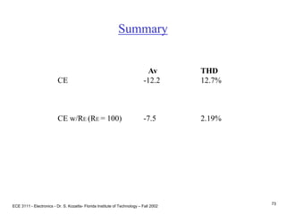
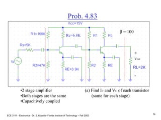
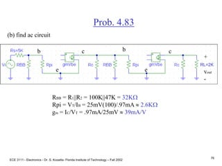
![ECE 3111 - Electronics - Dr. S. Kozaitis- Florida Institute of Technology – Fall 2002
75
Prob. 4.83
(a) Find IC and VC of each transistor
(same for each stage)
B-E voltage loop
VBB = IBRBB + VBE + IERE
where RBB = R1||R2 = 32K
VBB = VCCR2/(R1+R2) = 4.8V, and
IB IE/b
IE = [VBB - VBE ]/[RBB/b + RE]
IE = 0.97mA
VC = VCC - ICRC
VC = 15 - .97(6.8)
VC = 8.39V
+
VC
-](https://image.slidesharecdn.com/bjttransistors-converted-190816025303/85/Bjt-transistors-converted-76-320.jpg)
![ECE 3111 - Electronics - Dr. S. Kozaitis- Florida Institute of Technology – Fall 2002
77
Prob. 4.83
b c
e
+
vout
-
(c) find Rin1
Rin1 = RBB||Rpi
= 32K||2.6K
= 2.4KW
b c
e
Rin1
(d) find Rin2
Rin2 = RBB||Rpi
= 2.4KW
Rin2
find vb1/vi
= Rin1/[Rin1 + RS]
= 2.4K/[2.4K + 5K]
= 0.32
+
vb1
-
find vb2/vb1
vb2 = -gmvbe1[RC||RBB||Rpi]
vb2/vbe1 = -gm[RC||RBB||Rpi]
vb2/vb1 = -(39mA/V)[6.8||32K||2.6K]
= -69.1
+
vb2
-
RL=2K](https://image.slidesharecdn.com/bjttransistors-converted-190816025303/85/Bjt-transistors-converted-78-320.jpg)
![ECE 3111 - Electronics - Dr. S. Kozaitis- Florida Institute of Technology – Fall 2002
78
Prob. 4.83
b c
e
+
vout
-
(e) find vout/vb2
vout = -gmvbe2[RC||RL]
vout/vbe2 = -gm[RC||RL]
vb2/vb1 = -(39mA/V)[6.8K||2K]
= -60.3
b c
e
(f) find overall voltage gain
vout/vi = (vb1/vi) (vb2/vb1) (vout/vb2)
vout/vi = (0.32) (-69.1) (-60.3)
vout/vi = 1332
+
vb1
-
+
vb2
-
RL=2K](https://image.slidesharecdn.com/bjttransistors-converted-190816025303/85/Bjt-transistors-converted-79-320.jpg)
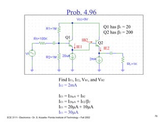
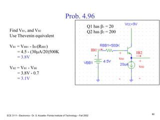
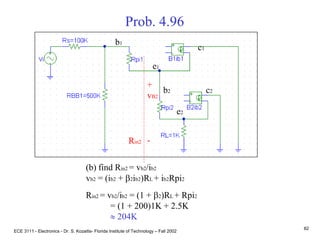
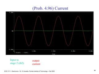
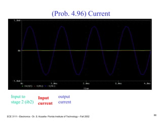
![ECE 3111 - Electronics - Dr. S. Kozaitis- Florida Institute of Technology – Fall 2002
81
Prob. 4.96
(b) find vout/vb2
vout = (ib2 + b2ib2)RL
vb2 = (ib2 + b2ib2)RL + ib2Rpi2
vout/vb2 = (1 + b2)RL/[(1 + b2)RL + Rpi2]
= (1 + 200)1K/[(1 + 200)1K+ 2.5K]
0.988
b1
e1
c1
b2
e2
c2
+
vout
-
+
vB2
-
Rpi2 = VT/IB2
= VT b2/IE2
= 25mV(200)/2mA
= 2.5KW](https://image.slidesharecdn.com/bjttransistors-converted-190816025303/85/Bjt-transistors-converted-82-320.jpg)
![ECE 3111 - Electronics - Dr. S. Kozaitis- Florida Institute of Technology – Fall 2002
83
Prob. 4.96
(c) find Rin1 = RBB1||(vb1/ib1)
= RBB1|| [ib1Rpi1 +(ib1 + b1ib1)Rin2]/ib1
= RBB1|| [Rpi1 +(1+ b1)Rin2],
where Rpi1 = VT b1/IE1 = 25mV(20)/30mA = 16.7K
= 500K||[16.7K + (1+ 20)204K]
500KW
b1
e1
c1
b2
e2
c2
+
vB1
-
Rin1
iB1](https://image.slidesharecdn.com/bjttransistors-converted-190816025303/85/Bjt-transistors-converted-84-320.jpg)
![ECE 3111 - Electronics - Dr. S. Kozaitis- Florida Institute of Technology – Fall 2002
84
Prob. 4.96
(c) find ve1/vb1
ve1 = (ib1 + b1ib1)Rin2
vb1 = (ib1 + b1ib1)Rin2 + ib1Rpi1
ve1/vb1 = (1 + b1) Rin2 /[(1 + b1) Rin2 + Rpi1]
= (1 + 20)204K/[(1 + 20)204K+ 16.7K]
0.996
b1
e1
c1
b2
e2
c2
+
ve1
-
iB1+
vB1
-](https://image.slidesharecdn.com/bjttransistors-converted-190816025303/85/Bjt-transistors-converted-85-320.jpg)
![ECE 3111 - Electronics - Dr. S. Kozaitis- Florida Institute of Technology – Fall 2002
85
Prob. 4.96
(d) find vb1/vi
vb1/vi = Rin1/[RS + Rin1]
= 0.82
b1
e1
c1
b2
e2
c2
+
vb1
-
(e) find overall voltage gain
vout/vi = (vb1/vi) (ve1/vb1) (vout/ve1)
vout/vi = (0.82) (0.99) (0.99)
vout/vi = 0.81](https://image.slidesharecdn.com/bjttransistors-converted-190816025303/85/Bjt-transistors-converted-86-320.jpg)


![Multisim_simulation_project_3_^0_4[1]-2.pptx](https://cdn.slidesharecdn.com/ss_thumbnails/multisimsimulationproject3041-2-240418183400-1d9cbd89-thumbnail.jpg?width=640&height=640&fit=bounds)


