Downloaded 303 times
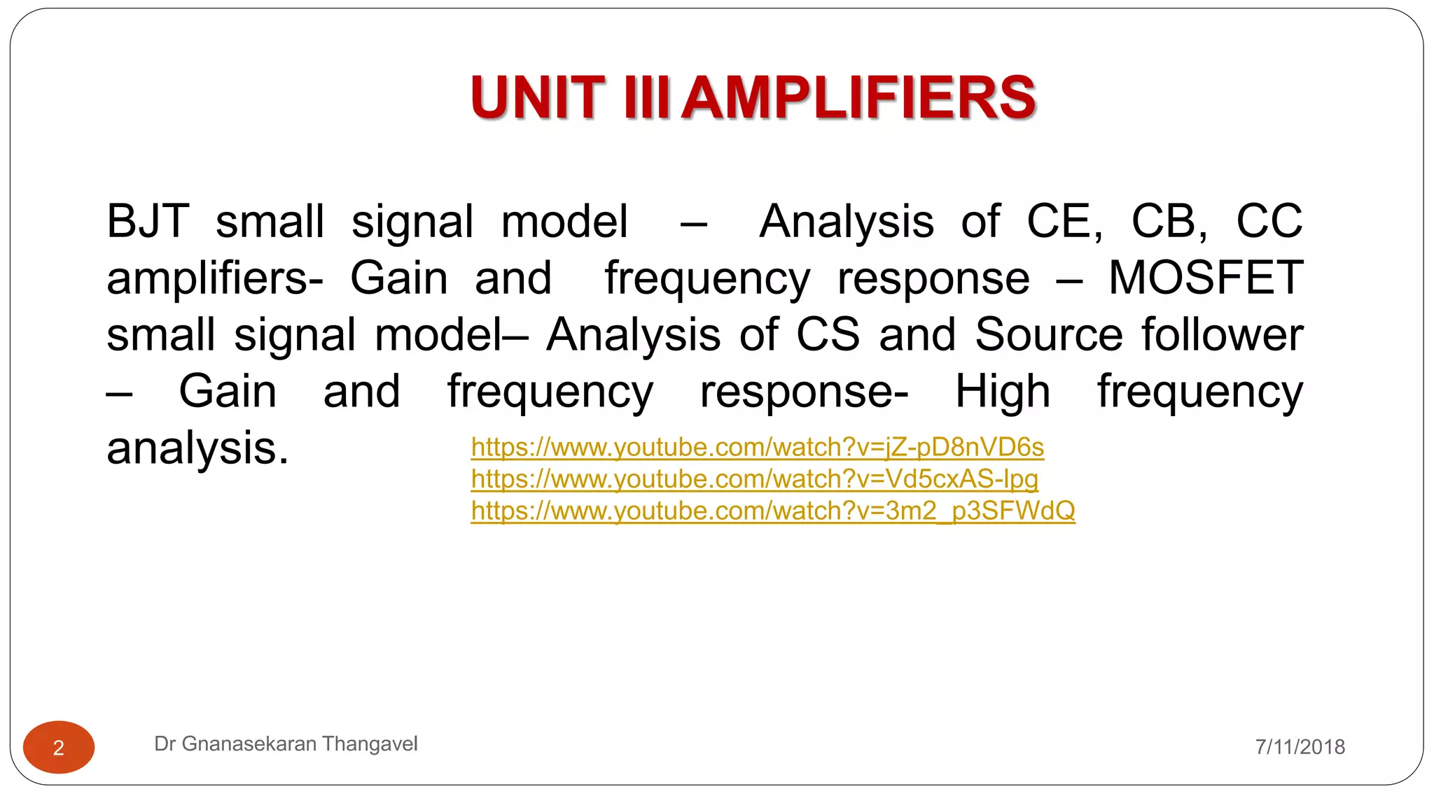
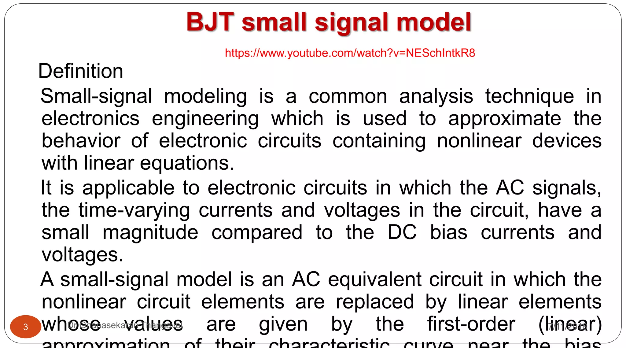
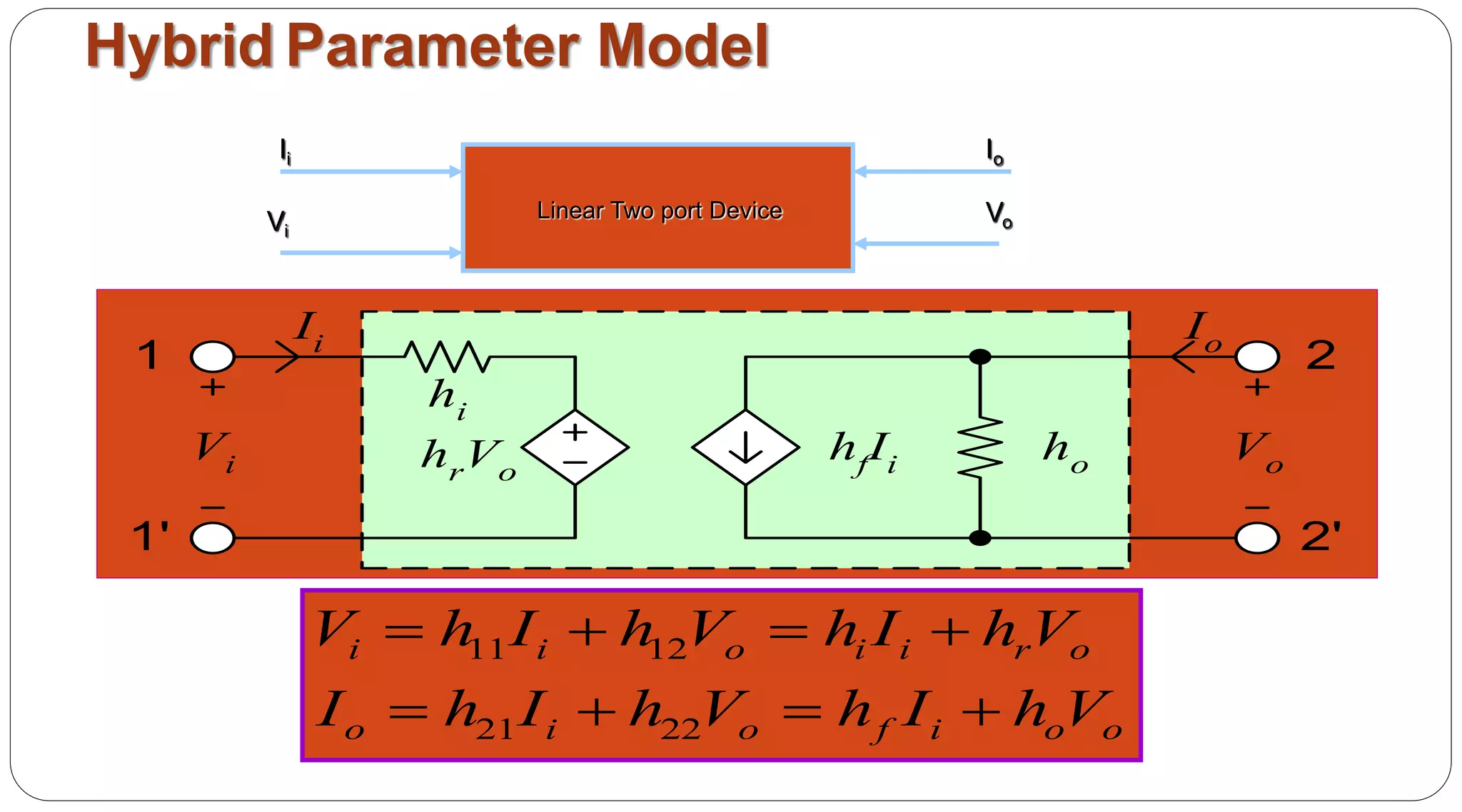
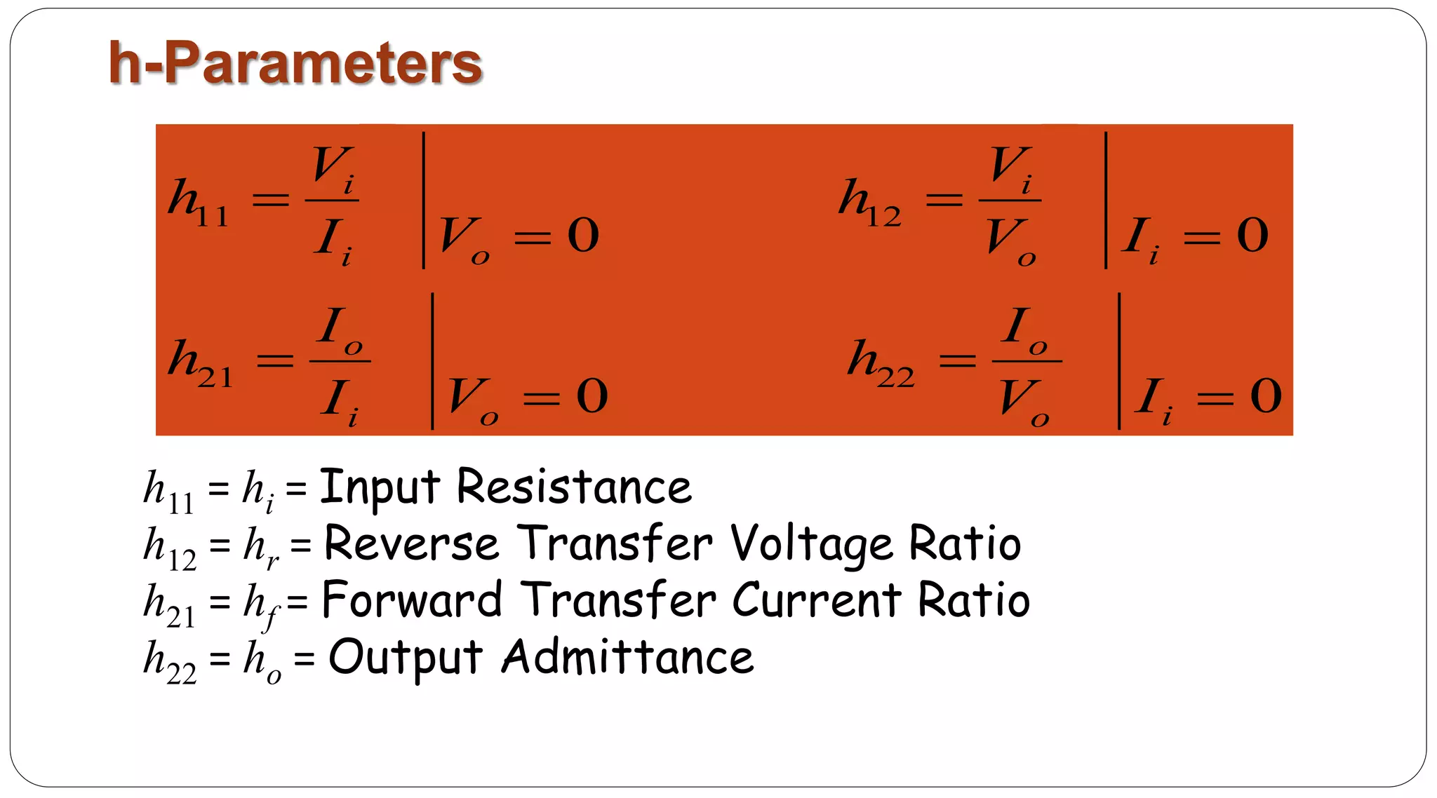
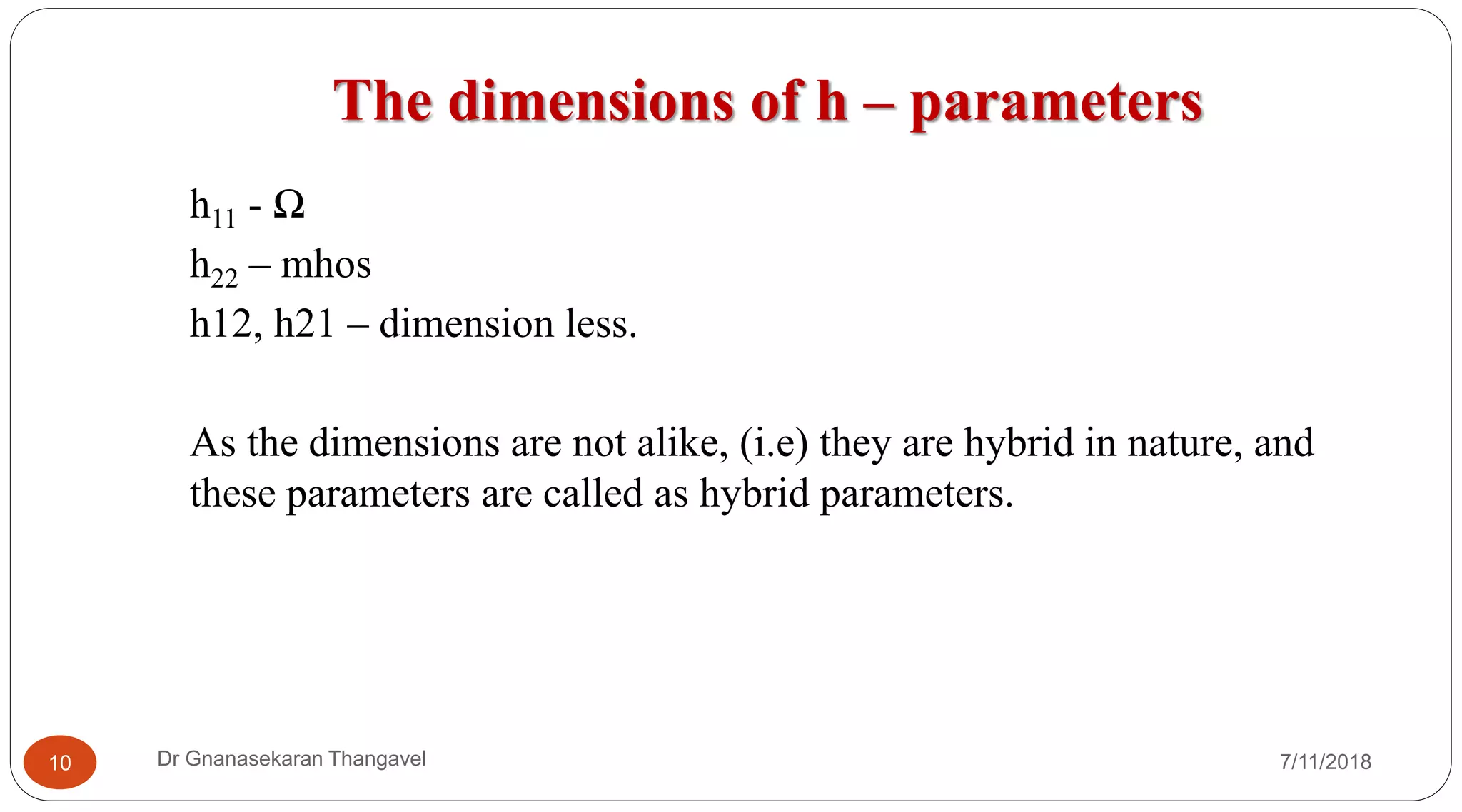
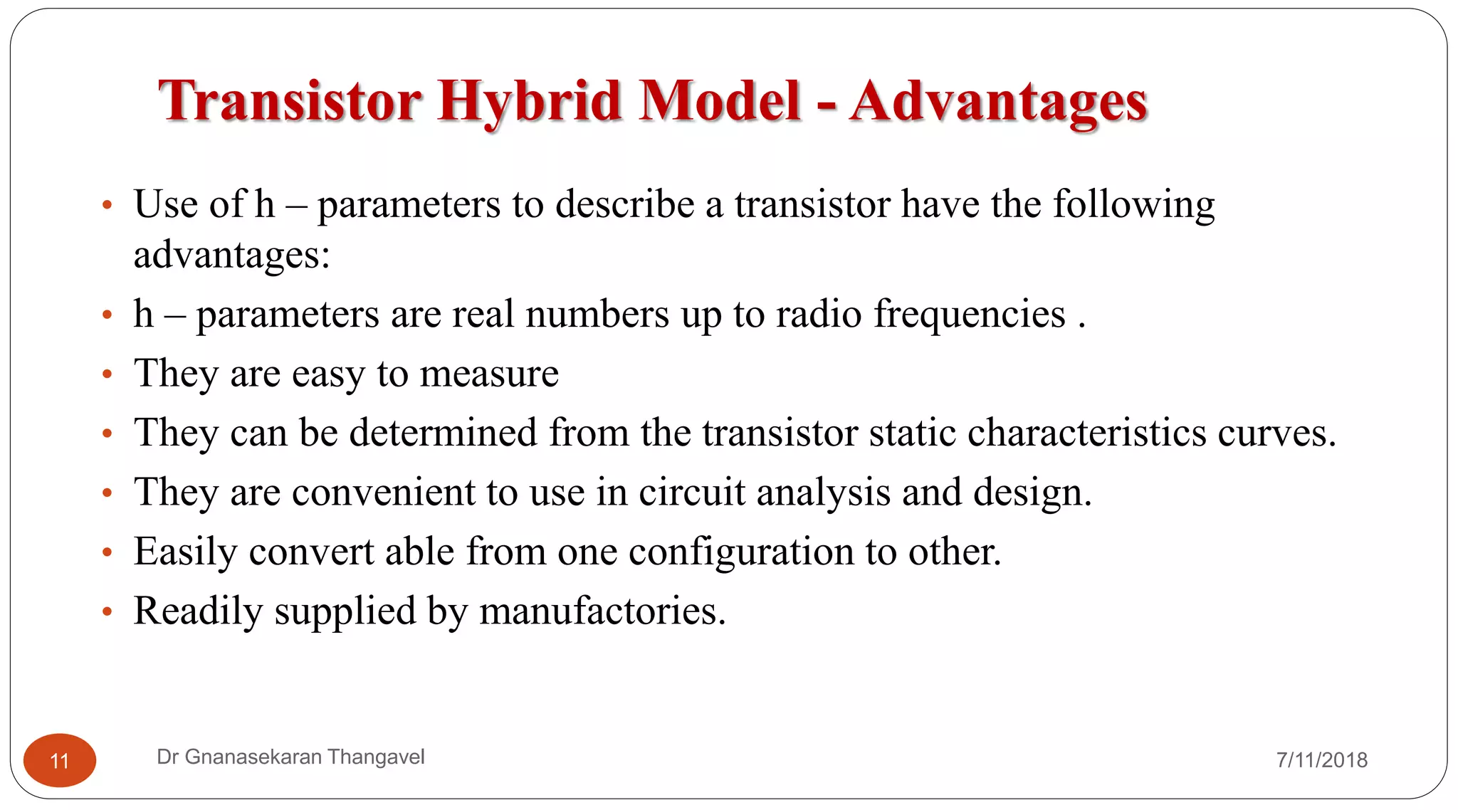
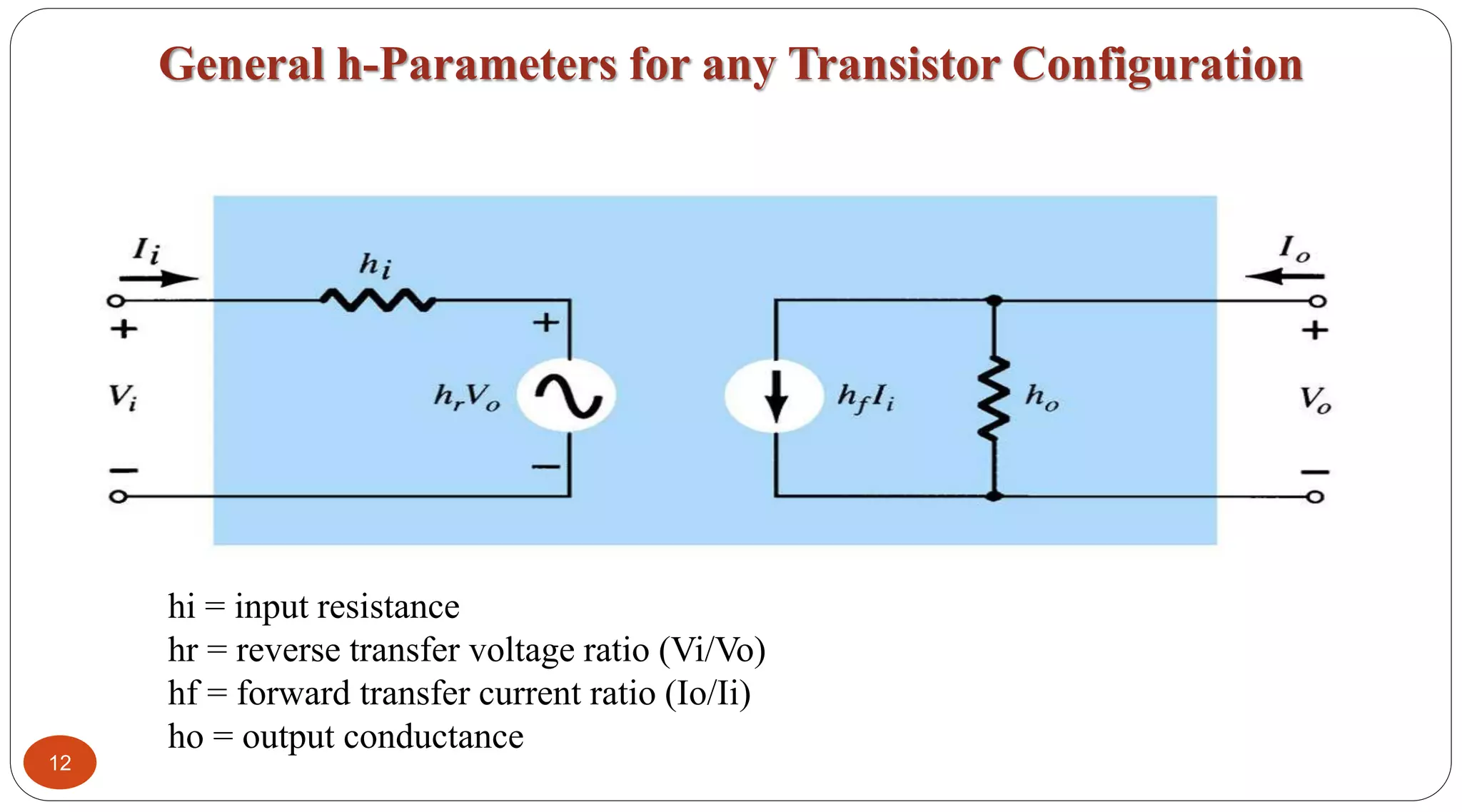
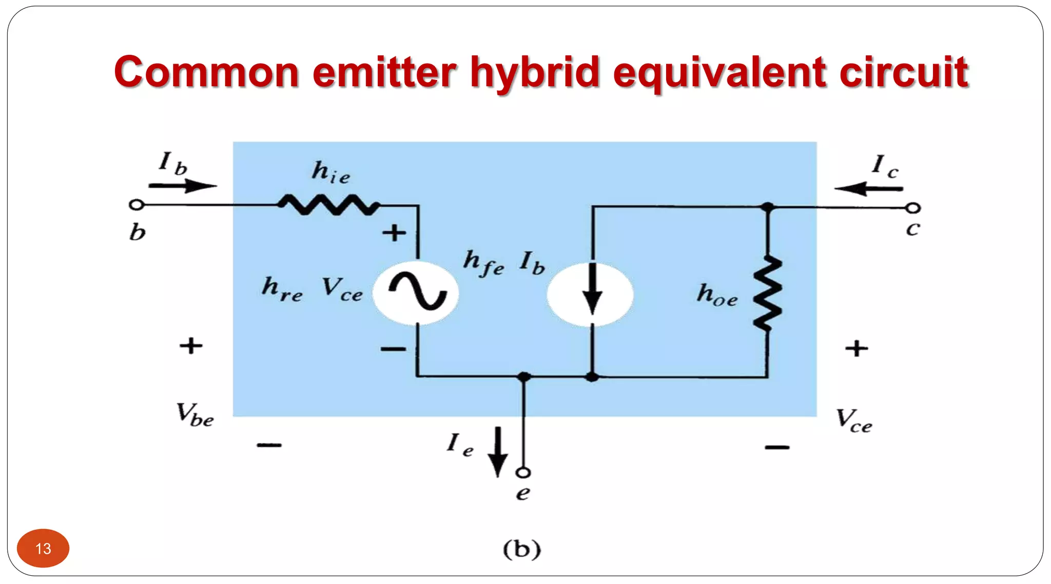
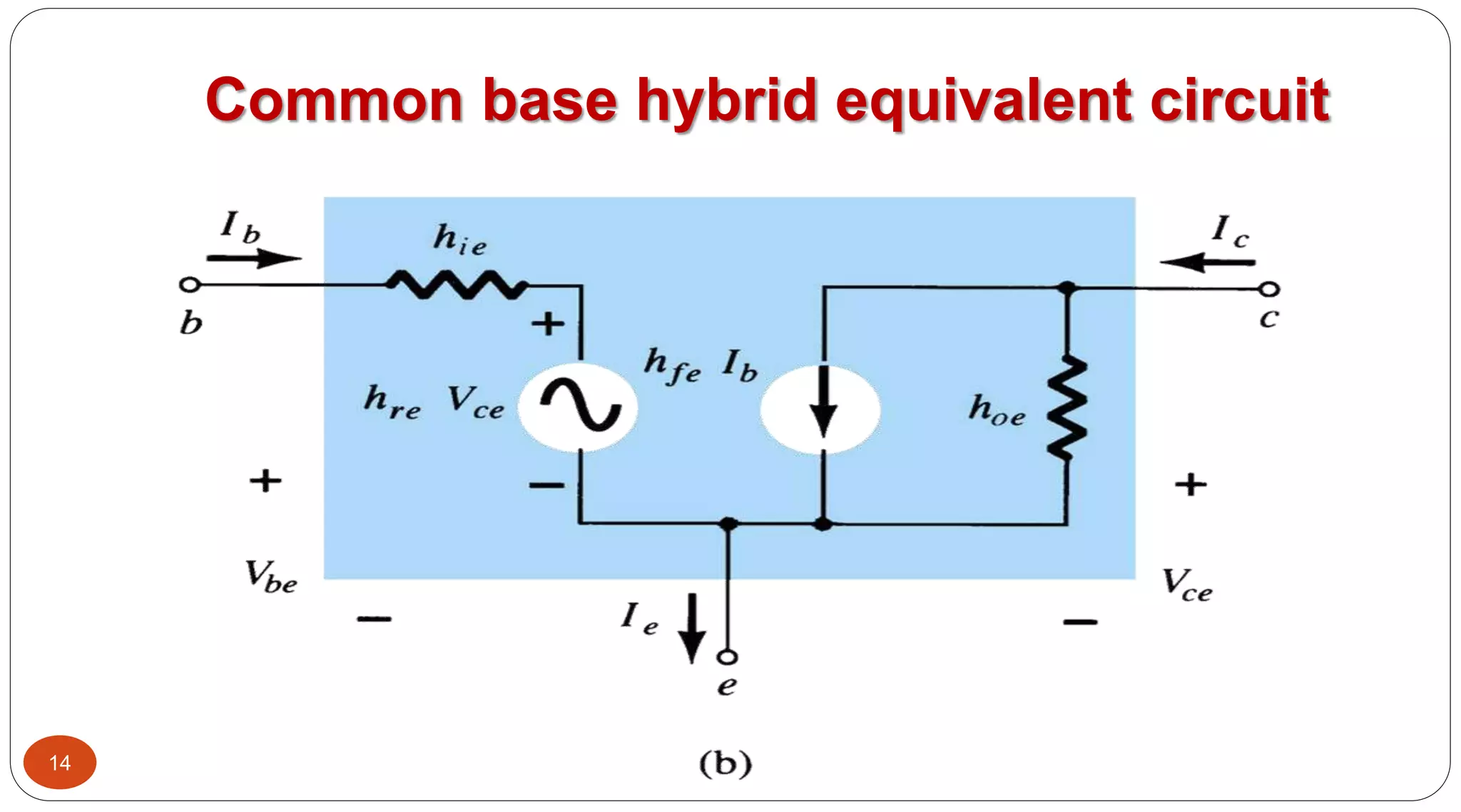
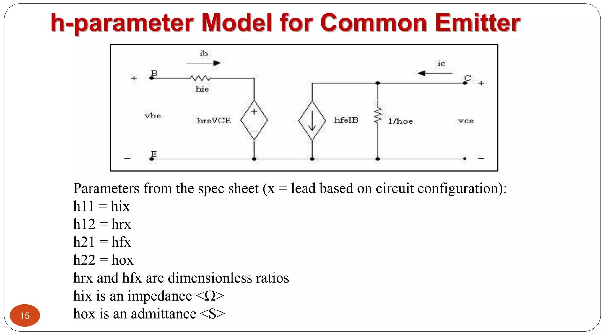
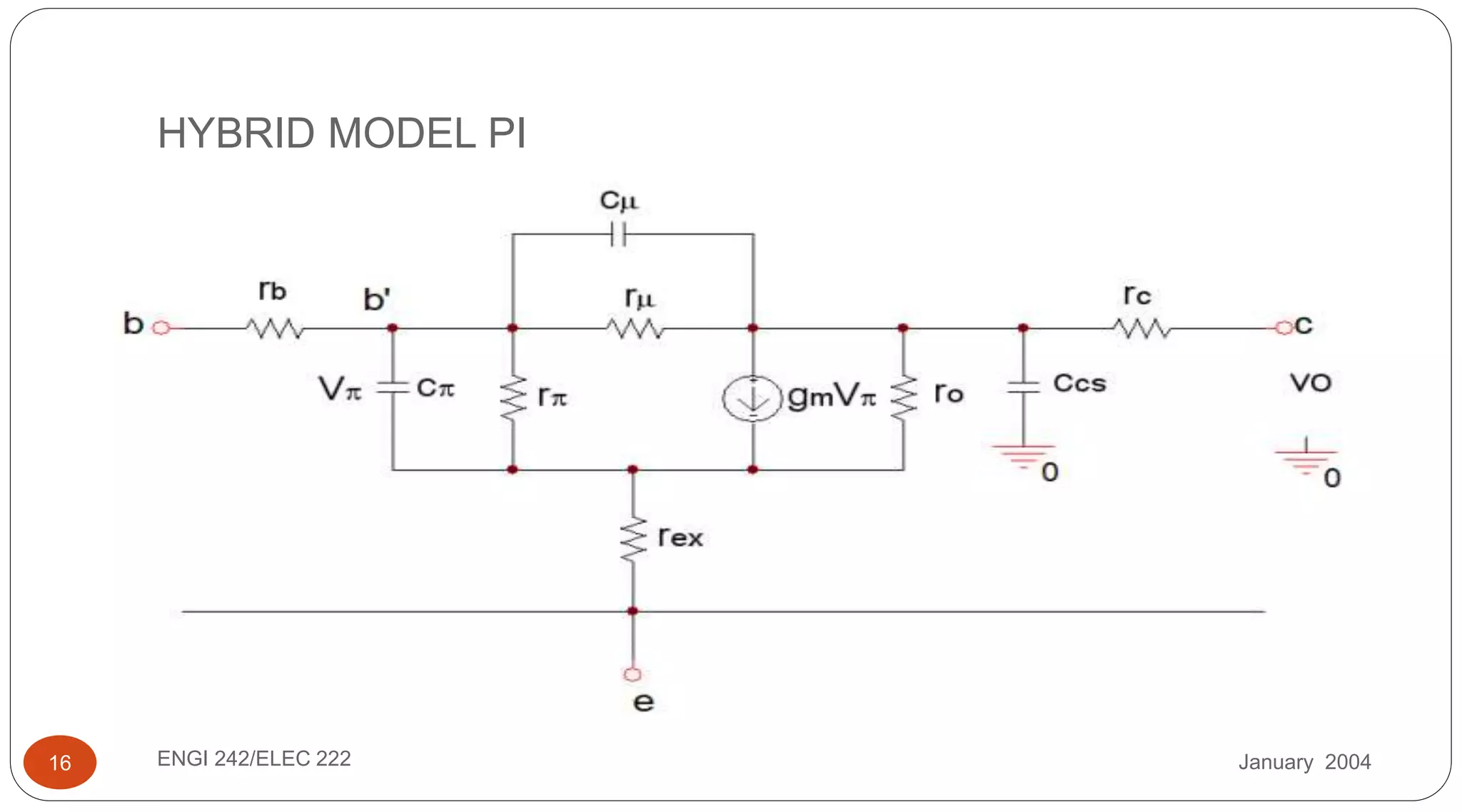
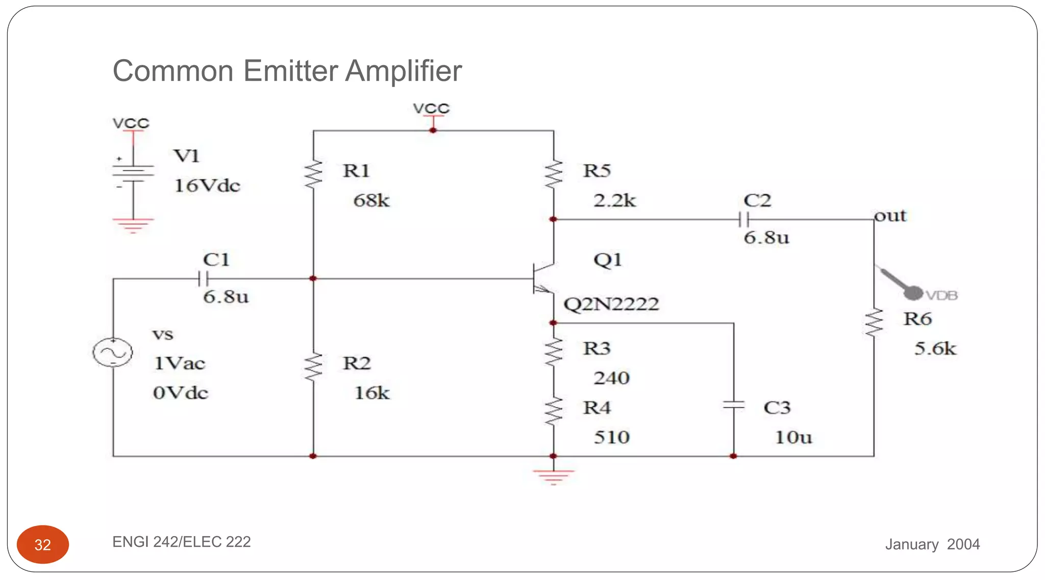
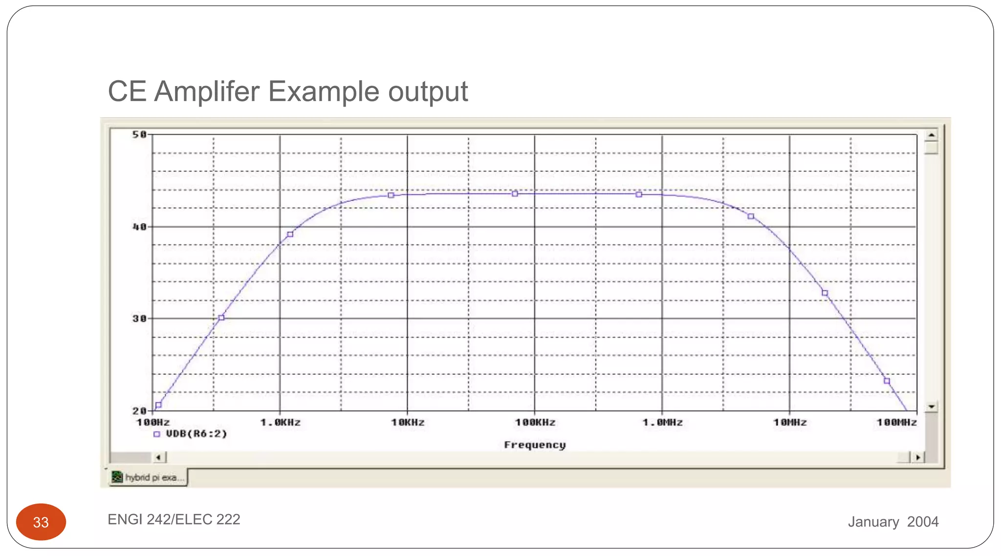
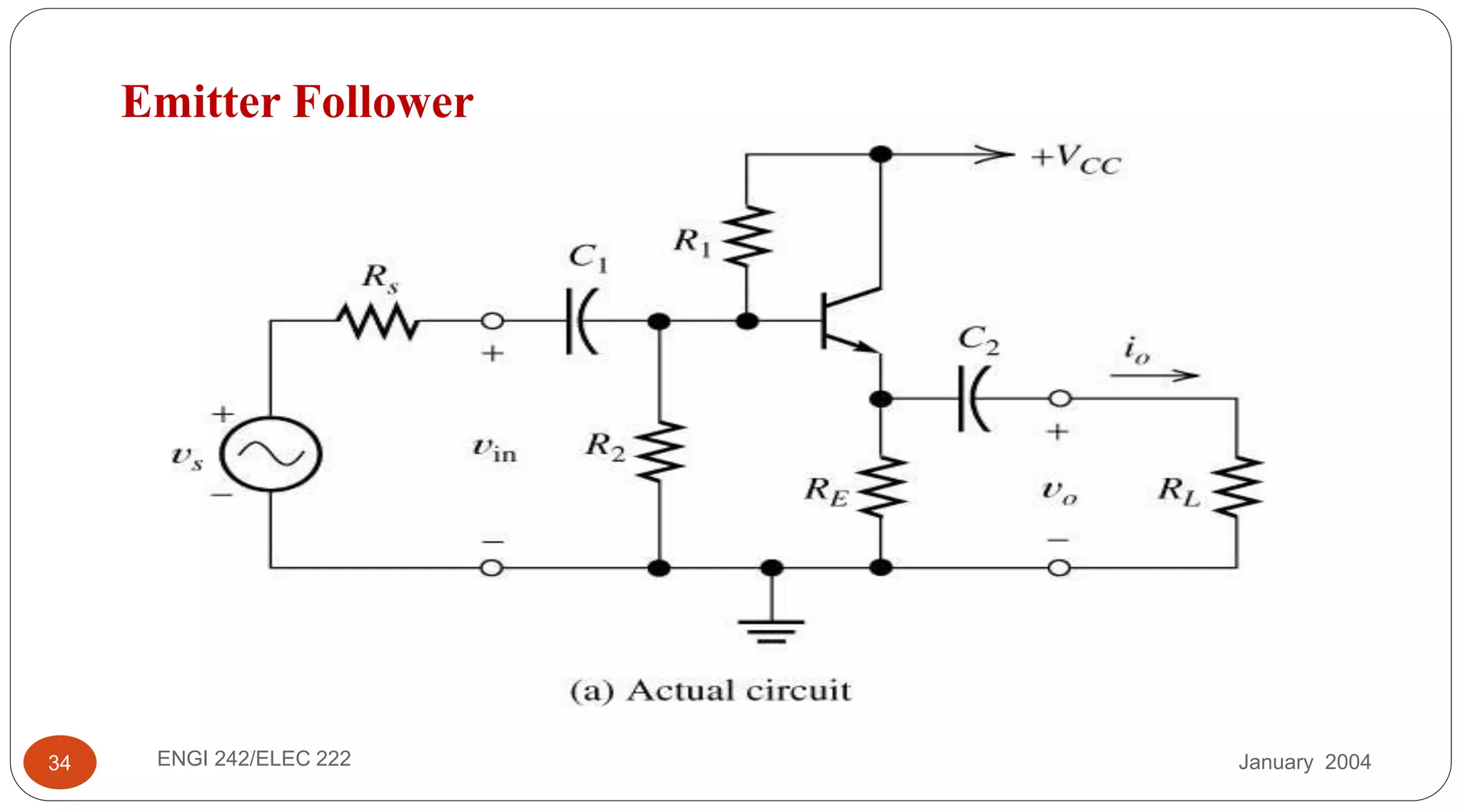
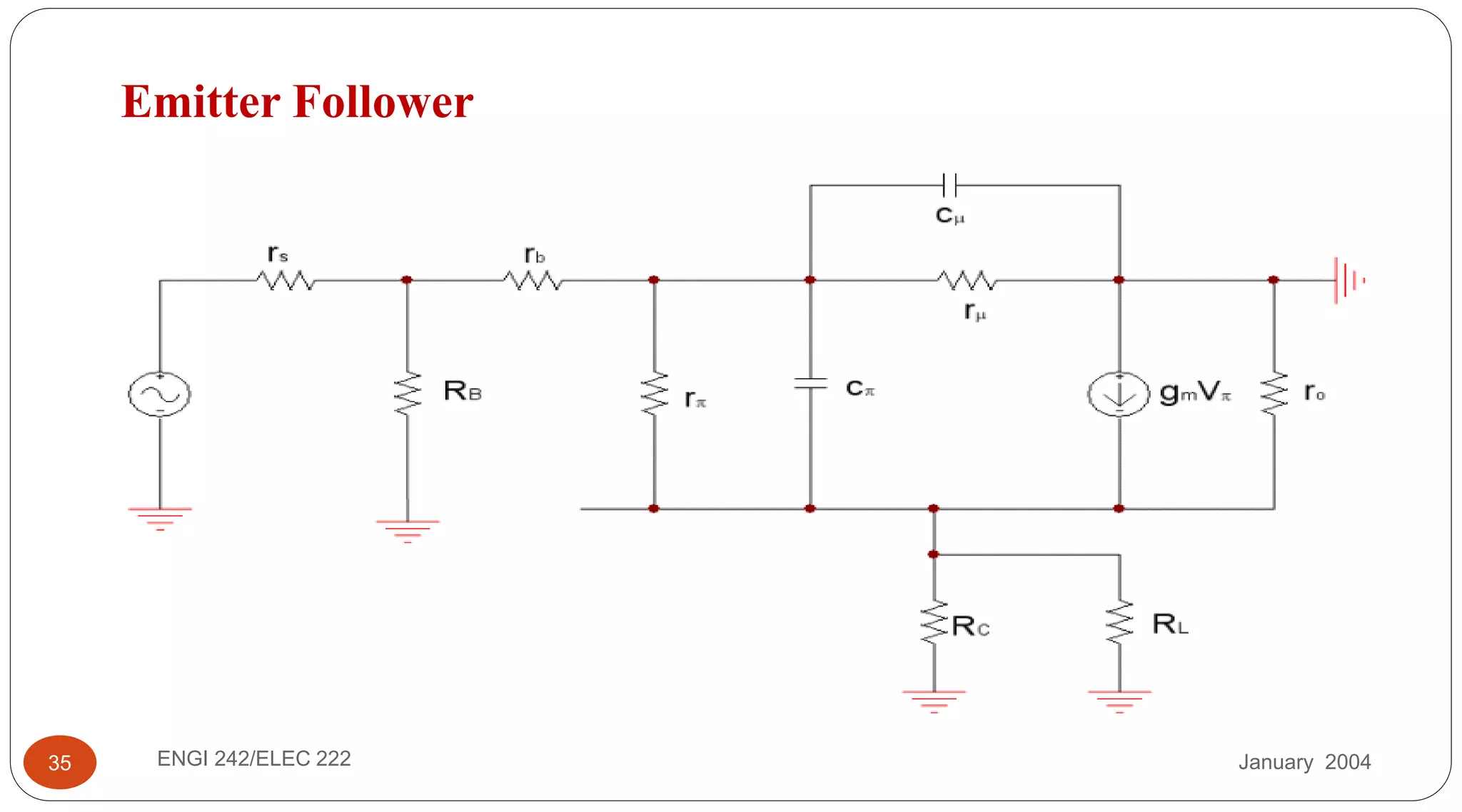
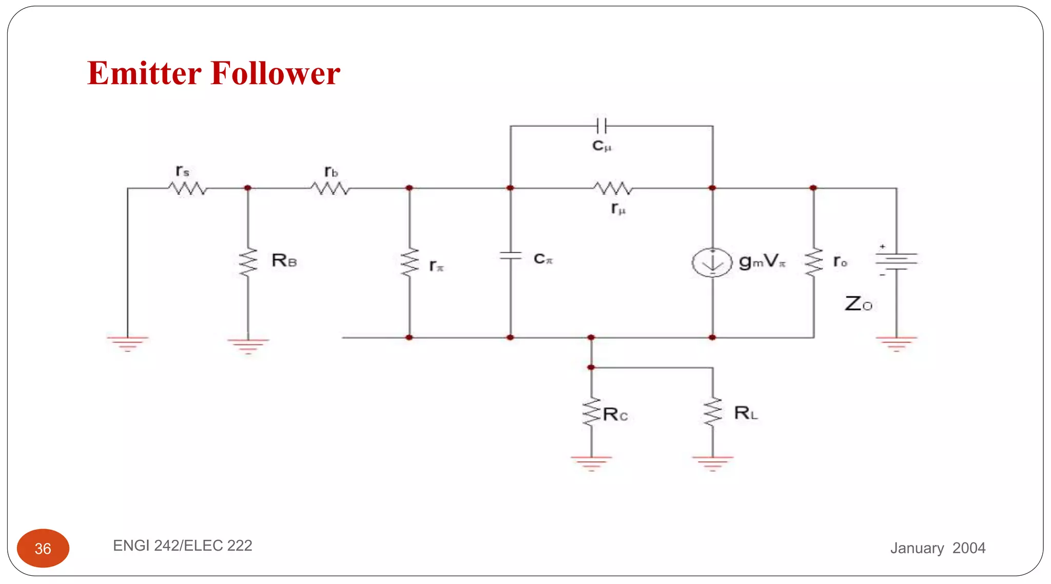
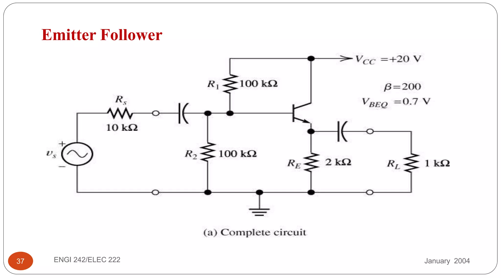
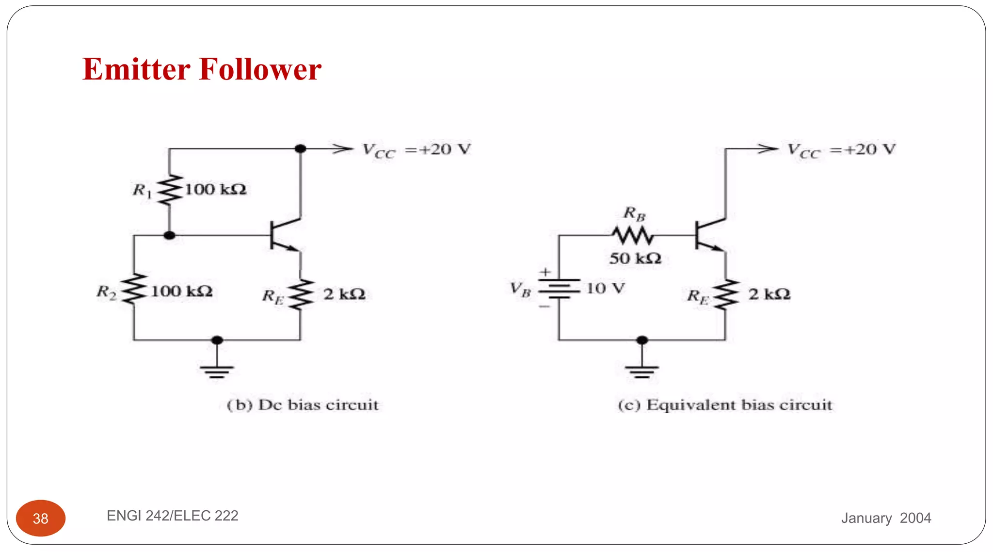
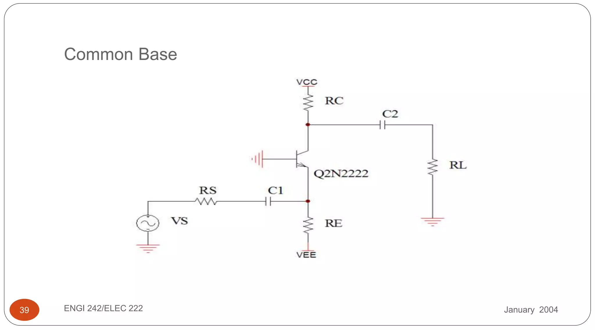
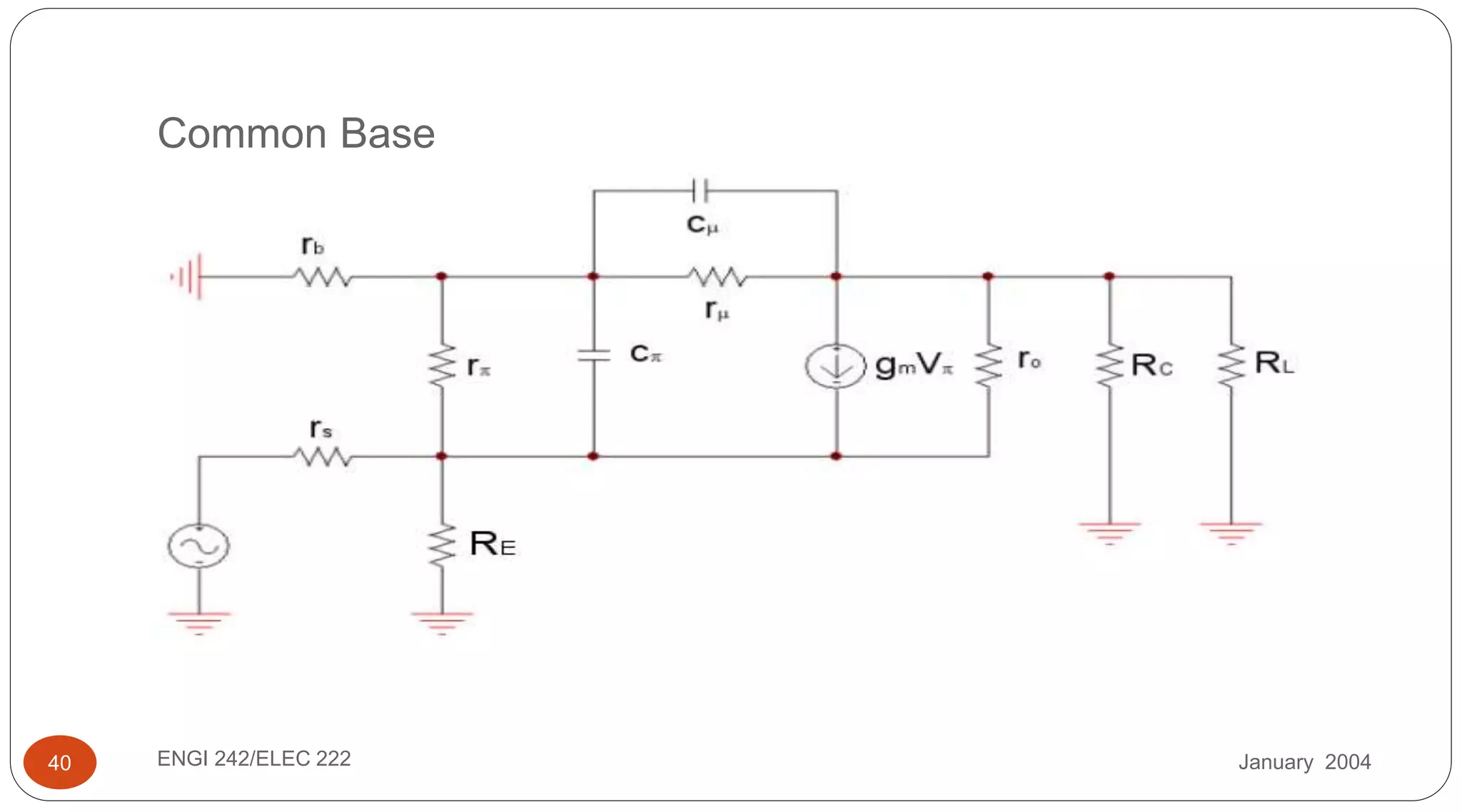


This document discusses amplifiers, specifically focusing on BJT (Bipolar Junction Transistor) and MOSFET (Metal-Oxide-Semiconductor Field-Effect Transistor) small signal models used for analyzing common emitter, common base, and common collector configurations. It covers the hybrid parameter model for transistors, including advantages, various parameters, and their applications in circuit analysis. Additionally, it includes links to video resources and references for further study in electronic devices and circuits.