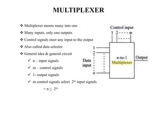
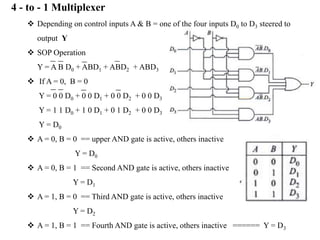
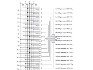
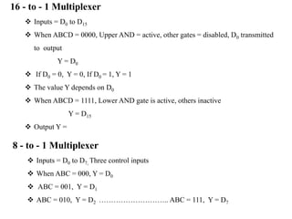
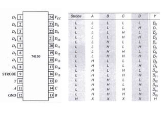
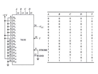
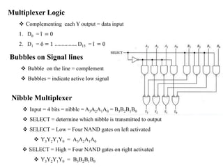
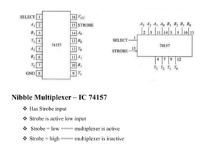
MULTIPLEXER
Dr. N. Anuradha
Asst. Professor of Physics
Bon Secours College for Women
Thanjavur
MULTIPLEXER
 Multiplexer means many into one
 Many inputs, only one outputs
 Control signals steer any input to the output
 Also called data selector
 General idea & general circuit
 n – input signals
 m – control signals
 1- output signals
 m control signals select 2m input signals
= n < 2m
4 - to - 1 Multiplexer
 Depending on control inputs A & B = one of the four inputs D0 to D3 steered to
output Y
 SOP Operation
Y = A B D0 + ABD1 + ABD2 + ABD3
 If A = 0, B = 0
Y = 0 0 D0 + 0 0 D1 + 0 0 D2 + 0 0 D3
Y = 1 1 D0 + 1 0 D1 + 0 1 D2 + 0 0 D3
Y = D0
 A = 0, B = 0 == upper AND gate is active, others inactive
Y = D0
 A = 0, B = 1 == Second AND gate is active, others inactive
Y = D1
 A = 1, B = 0 == Third AND gate is active, others inactive
Y = D2
 A = 1, B = 1 == Fourth AND gate is active, others inactive ====== Y = D3
16 - to - 1 Multiplexer
 Inputs = D0 to D15
 When ABCD = 0000, Upper AND = active, other gates = disabled, D0 transmitted
to output
Y = D0
 If D0 = 0, Y = 0, If D0 = 1, Y = 1
 The value Y depends on D0
 When ABCD = 1111, Lower AND gate is active, others inactive
Y = D15
 Output Y =
8 - to - 1 Multiplexer
 Inputs = D0 to D7, Three control inputs
 When ABC = 000, Y = D0
 ABC = 001, Y = D1
 ABC = 010, Y = D2 ……………………….. ABC = 111, Y = D7
IC 74150
 16 - to - 1 TTL multiplexer, 24 pin IC
 Pin 1 to 8 & 16 to 23 ===== D0 to D15
 Pin 11, 13, 14, 15 ======= A, B, C, D
 Pin 10 = output = complement of the selected data bit
 Pin 9 = Strobe = enables or disables the input
 Low strobe = enable the multiplexer ====== Y = Dn
 High strobe = disable the multiplexer ====== Output = high === value of
ABCD doesn’t matter
 Two standard methods for implementing truth table
1. Sum of products
2. Product of sum
3. Third method is multiplexer solution
 i.e., complementing each Y output = data input
Multiplexer Logic
 Complementing each Y output = data input
1. D0 = î = 0
2. D1 = ô = 1 ……………. D15 = î = 0
Bubbles on Signal lines
 Bubble on the line = complement
 Bubbles = indicate active low signal
Nibble Multiplexer
 Input = 4 bits = nibble = A3A2A1A0 = B3B2B1B0
 SELECT = determine which nibble is transmitted to output
 SELECT = Low = Four NAND gates on left activated
 Y3Y2Y1Y0 = A3A2A1A0
 SELECT = High = Four NAND gates on right activated
 Y3Y2Y1Y0 = B3B2B1B0
Nibble Multiplexer – IC 74157
 Has Strobe input
 Strobe is active low input
 Strobe = low ==== multiplexer is active
 Strobe = high ==== multiplexer is inactive

3. multiplexer

  • 1.
    MULTIPLEXER Dr. N. Anuradha Asst.Professor of Physics Bon Secours College for Women Thanjavur
  • 2.
    MULTIPLEXER  Multiplexer meansmany into one  Many inputs, only one outputs  Control signals steer any input to the output  Also called data selector  General idea & general circuit  n – input signals  m – control signals  1- output signals  m control signals select 2m input signals = n < 2m
  • 3.
    4 - to- 1 Multiplexer  Depending on control inputs A & B = one of the four inputs D0 to D3 steered to output Y  SOP Operation Y = A B D0 + ABD1 + ABD2 + ABD3  If A = 0, B = 0 Y = 0 0 D0 + 0 0 D1 + 0 0 D2 + 0 0 D3 Y = 1 1 D0 + 1 0 D1 + 0 1 D2 + 0 0 D3 Y = D0  A = 0, B = 0 == upper AND gate is active, others inactive Y = D0  A = 0, B = 1 == Second AND gate is active, others inactive Y = D1  A = 1, B = 0 == Third AND gate is active, others inactive Y = D2  A = 1, B = 1 == Fourth AND gate is active, others inactive ====== Y = D3
  • 5.
    16 - to- 1 Multiplexer  Inputs = D0 to D15  When ABCD = 0000, Upper AND = active, other gates = disabled, D0 transmitted to output Y = D0  If D0 = 0, Y = 0, If D0 = 1, Y = 1  The value Y depends on D0  When ABCD = 1111, Lower AND gate is active, others inactive Y = D15  Output Y = 8 - to - 1 Multiplexer  Inputs = D0 to D7, Three control inputs  When ABC = 000, Y = D0  ABC = 001, Y = D1  ABC = 010, Y = D2 ……………………….. ABC = 111, Y = D7
  • 7.
    IC 74150  16- to - 1 TTL multiplexer, 24 pin IC  Pin 1 to 8 & 16 to 23 ===== D0 to D15  Pin 11, 13, 14, 15 ======= A, B, C, D  Pin 10 = output = complement of the selected data bit  Pin 9 = Strobe = enables or disables the input  Low strobe = enable the multiplexer ====== Y = Dn  High strobe = disable the multiplexer ====== Output = high === value of ABCD doesn’t matter  Two standard methods for implementing truth table 1. Sum of products 2. Product of sum 3. Third method is multiplexer solution  i.e., complementing each Y output = data input
  • 9.
    Multiplexer Logic  Complementingeach Y output = data input 1. D0 = î = 0 2. D1 = ô = 1 ……………. D15 = î = 0 Bubbles on Signal lines  Bubble on the line = complement  Bubbles = indicate active low signal Nibble Multiplexer  Input = 4 bits = nibble = A3A2A1A0 = B3B2B1B0  SELECT = determine which nibble is transmitted to output  SELECT = Low = Four NAND gates on left activated  Y3Y2Y1Y0 = A3A2A1A0  SELECT = High = Four NAND gates on right activated  Y3Y2Y1Y0 = B3B2B1B0
  • 10.
    Nibble Multiplexer –IC 74157  Has Strobe input  Strobe is active low input  Strobe = low ==== multiplexer is active  Strobe = high ==== multiplexer is inactive