Unit-VI
Introduction to DSP Processors
Dr.G.Anandbabu
Dept of ECE
MVR College of Engineering and Technology
Paritala
In 1979, Intel introduced the first Digital Signal
Processor (The Intel 2920), featuring on-chip ADC and DACs. Texas
instruments introduced the TMS32010 the first generation fixed point DSP in
the TMS320family. Later it introduced TMS320C20. Note that TMS32010
family does not have C in it because it was originally designed in NMOS
technology whereas all the other DSPs are designed with CMOS technology.
The programmable digital signal processors (PDSPs) are
general purpose microprocessors designed specifically for digital signal
processing applications. They contain special architecture and instruction set so
as to execute computation-intensive DSP algorithms more efficiently. The
programmable DSPs can be divided into two broad categories. They are
1.General purpose digital signal processors
2.Special purpose digital signal processors.
General purpose digital signal processors:-
These are basically high speed microprocessors with
architecture and instruction sets optimized for DSP operations. They Include
fixed point processors such as Texas Instruments TMS320C5x, TMS320C54x
and Motorola, DSP563x and floating point processors such as Texas
instruments TMS320C4x,TMS320C67xx and analog devices ADSP21xxx.
Special purpose digital signal processors:-
These type of processors consist of hardware
1.Designed for specific DSP algorithms such as FFT.
2.Hardware designed for specific applications such as PCM and filtering.
Examples:
MT93001(Mitel’s multi channel telephony voice echo canceller)
PDSP16515A, TM-44,TM-66 (FFT processors)
UPDSP 16256,Model 3092(programmable FIR filter)
Texas Instruments DSP History:-
1982 TMS32010:
• first programmable general-purpose DSP to market
• Operating at 5 MIPS.
• It was ideal for modems and defense applications
1988 TMS320C3x:
• TI introduces the industry’s first floating-point DSP.
• High-performance applications demanding floating-point performance
include voice/fax mail, 3-D graphics, bar-code scanners and video
conferencing audio and visual systems.
1988 TMS320C1x: the world’s first DSP-based hearing aid uses TI’s DSP.
TMS320C3x: first 32-bit floating point DSP processor.
TMS320C4x: 32 bit Floating point DSP processor optimized for parallel
processing
1989 TMS320C5x:
• TI introduces highest performance fixed-point DSP generation in the
industry,
• operating at 28 MIPS
• The ‘C5x delivers 2 to 4 times the performance of any other fixed-point
DSP.
• Targeted to the industrial, communications, computer and automotive
segments.
• Accepts the source code from C1X, C2X, C2XX generations.
• Faster cycle rate.
• On-chip memory.
• Parallel logic unit(PLU).
• The ‘C5x DSPs are used mainly in
• cellular and cordless telephones,
• high-speed modems,
• printers and copiers.
• 1992 DSPs become one of the fastest growing segments within the
automobile electronics market.
Selecting Digital Signal processor:-
• Architectural Features:- Good Architectural features includes
size of on-chip memory, special instructions & I/O capability.
• Execution Speed:- Execution speed is measured in terms of the
Clock Speed in MHz & the no. of instructions executing: MIPS,
MELOPS(Millions of floating point operations per second).
• Type of Arithmetic :- 1. Fixed point 2. Floating point; in
general floating point arithmetic DSP processors more expensive
but preferred most.
• Word length:- 16-bit or 32-bit(24-bit mantissa, 8-bit exponent)
System architectures:-
• The system’s architecture represents the way that the elements of
the system are interconnected and exchange data. It has a
significant influence on the way the CPU accesses its peripherals.
Every type of architecture requires special hardware features from
the CPU (in particular from its bus system). Every type of
architecture includes:
• At least one CPU
• At least one peripheral
• At least one bus system connecting the CPU to the peripherals.
VON NEUMANN ARCHITECTURE:-
• In 1946, well before the development of the first
microprocessor, John Von Neumann developed the first computer
architecture that allowed the computer to be programmed by codes
residing in memory. In this the program instructions are stored in Read
Only Memory (ROM). The Von Neumann architecture is the most
widely used today, and is implemented by the majority of microprocessors
on the market. In a computer with Von Neumann Architecture, the
CPU can be either reading an instruction or reading/ writing data
from/to the memory. But both the operations cannot be occurs at at a
time. The Von Neumann architecture is shown below:
• This architecture consists of Three Buses.
• Data Bus
• Address Bus
• Control Bus.
• All these buses are on the Single Bus System.
1.Data Bus:- Transports data between the CPU and its peripherals. It is bi-directional.
The CPU can read or write data in the peripherals using this bus.
2.Address Bus:- The CPU uses the address bus to indicate which peripherals it wants
to access, and within each peripheral which is specific register. The address bus is
unidirectional The CPU always writes the address, which is read by the
peripherals.
3.Control Bus:- This bus carries signals that are used to manage and synchronize
the exchanges between the CPU and its peripherals. For instance the signal that
indicates if the CPU wants to read or write the peripheral, as well as the signal used
to synchronize the exchange are part of the control bus. Since the CPU initiates and
manages all data exchanges with the peripherals, the main signals of the control bus
originate at the CPU and are sent to the peripherals. However special lines of the
control bus, such as interrupt or wait-state signals carry information from the
peripherals to the CPU.
•
The main characteristic of the Von Neumann architecture is that it
only possesses 1 bus system. The same bus carries all the
information exchanged between the CPU and the peripherals,
including the instruction codes as well as the data processed by the
CPU. This is main disadvantage of this architecture
HARVARD ARCHITECTURE1940
• The Harvard architecture as the name implies that it was developed at
Harvard University. By contrast to the Von Neumann architecture, it uses
two separate bus systems to transport the instruction codes and the data
being processed by the CPU.
• The Program Bus System: Is used exclusively to transport instruction codes
from the program memory to the CPU during the fetch cycle.
• The Data Bus System: Is used exclusively to transport data from/to the
CPU, to/from the memory and peripherals.
The Harvard Architecture physically separates the memories for programs &
Data as shown in below.
An alternate block diagram of this architecture is shown below
In this architecture there are two separate buses for the program and
data memory.
Hence the content of programmed memory and
data memory can be accessed in parallel. The instruction code can be fed
from the program memory to the control unit while the operand is fed to the
processing unit from the data memory. The processing unit consist of the
registers and processing elements such as MAC units, multiplier, ALU, Shifters
etc.
The programmable DSPs follow the modified Harvard architecture which is
shown
In this modified Architecture, One Address bus is used to access both
data memory & Program memory. Other Address bus is used to access the Data
memory only. Data can also be transferred from one memory to another. By
using more no. of buses, no. of accesses/ clock cycle is increased with Harvard
Architecture. Examples of Processors that are uses this architecture are
TMS320C54X Uses 4-Address buses, Motorola 5600x, 96002 uses separate buses.
VERY LONG INSTRUCTION WORD(VLIW)
ARCHITECTURE:-
• The new attracted architecture that has great deal attention in
DSP processors is VLIW Architecture. Very long instruction
Word processing increases the no.of instructions that are
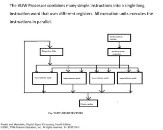
processed per cycle . VLIW processor consists of architecture
that reads relatively large group of instructions & executes
them at the same time using multiple execution units.
The VLIW Processor combines many simple instructions into a single long
instruction word that uses different registers. All execution units executes the
instructions in parallel.
Advatages of VLIW Architecture:-
•Increased performance.
•Potentially easier to program.
•Potentially scalable.
•Better compiler targets.
•Can add more execution units.
•Allow more instructions to be packed into the VLIW instruction.
Disadvantages of VLIWArchitecture:-
•High power consumption.
•Increased memory use.
•Compiler complexity.
•Misleading MIPS ratings.
•Program must keep track of instruction scheduling.
Multiplication and Accumulation:-
• The MAC is the most important components of the DSP Processor core . The
MAC performs iterative computations and supports double precision. It is the
module which implements the hardware supporting auto correlation, filtering
and transform functions. The convolution, the most common DSP instruction is
performed in the MAC.
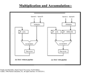
• The MAC as its name needs hardware to perform
multiplication and accumulation. The multiplication is done by a signed
multiplier and the accumulation of the multiplied value with a accumulator is
done by a adder. The multiplication and the accumulation can be done in the
same clock cycle. The cost of doing that would be a slower clock rate as the
multiplication would take a long time which slows down the clock rate. In this
design the instruction decoder is simple to design as the MAC will have the
same pipeline as the other blocks. By introducing a register after the
multiplication the MAC can be made a double cycle execution module as
shown in below:
Pipelining:-
• Most of the early microprocessors execute instructions entirely sequentially.
After the execution of first instruction the next one starts. The problem with
this is that it is extremely inefficient, since the second instruction has to wait
until all steps of first instruction are completed. To improve the efficiency,
advanced microprocessors & digital signal processors use an approach called
Pipelining in which different phases of operations & execution of instructions
are carried out in parallel. That is in modern processors the first step of
execution is performed on the first instruction & then when the instruction
phases to the next step, a new instruction is started. The steps in the pipeline
often called stages.
• “Fetching the next instruction while current instruction is
being under execution is called Pipelining”
The action of any microprocessor can be broken down into series of four
phases. They are
1.The Fetch phase(F): In which the next instruction is fetched from the
address stored in the program counter.
2. The Decode phase(D) :- In which the instruction In the instruction register
is decoded and the address in the program counter is incremented.
3.Memory read(R) phase:- Reads the data buses and also writes data to the
data buses.
4.The execute phase(X) :- executes the instruction currently in the instruction
register and also completes the write process.
The pipeline process is shown below for TMS320C54X has four stages of
pipelining.
Multiported Memory :-
The dual port memory has two independent data and address buses as shown in
the following fig.
•Two memory access is can be achieved in a clock period. Multiported
memory dispense with the need for storing the program and data in two
different memory chips in order to permit simultaneous access to both data
and program memory.
• E.g. Motorola DSP561XX processor has a single ported program memory
and a dual ported data memory.
Multiple Access Memory :-
• The number of memory accesses/clock period can be increased by using
a high-speed memory that permits more than one memory access/clock
period.
• e.g. The DARAM (dual access RAM) permits two memory access/clock
period. Multiple accesses may be connected to the processing units of the
P-DSPs by using the Harvard Architecture.
Addressing modes:-
Addressing modes form the basis for the AGU architecture. The addressing
modes are decided during the instruction set design. The most common
addressing modes used is DSP Processors are listed below.
1. Register Addressing: The register is used as the address pointer
2. Direct Addressing (Absolute Addressing): The address is a part of the
instruction. The user has the choice to directly specify the address in the
instruction.
3. Register post incremental: The address pointer will take a register value
and increment the register by a defined step or default ‘1’.
4. Register post decrement: The address pointer will take a register value and
decrement the register by a defined step or default ‘1’.
5. Segment plus offset: The address pointer will take a register value added
with a defined offset from the instruction.
6. Indexed addressing: The address pointer will take a register value and add
indexed register value.
• The other special types of addressing modes are as below.
Modulo Addressing Mode
The FIR is the most frequently used DSP
function. The implementation of the FIR is a First in First out
(FIFO) buffer using a chain of registers. The chain of registers
in the FIFO implementation consumes a lot of power. To
avoid this FIFO implementation is replaced by the memories
in DSP Processors. But for the memory to function like a ring
buffer the FIFO address pointer will be shifted. This
addressing mode where the memory behaves like a FIFO ring
buffer is called modulo addressing.
Bit Reversed Addressing Mode
• The Fast Fourier Transform (FFT) is the one of the frequently used DSP
algorithms in modern DSP applications. The FFT computation can be
computed in Decimation in Time (DIT) or Decimation in Frequency (DIF).
Both algorithms have the same addressing mode and also the same number
of computations. The DIT algorithm involves nested loops for
computations. After computation as per the algorithm it will be noticed that
the bits are in the reverse order for the addressing. The MBS must be
swapped with the LSB, (MSB-1) with (LBS-1) and so on until the bit
integer is reversed. This addressing mode that supports FFT computation is
called bit reversed addressing mode. At the HW level this is a very simple
implementation of bit assignment and the cost is negligible.