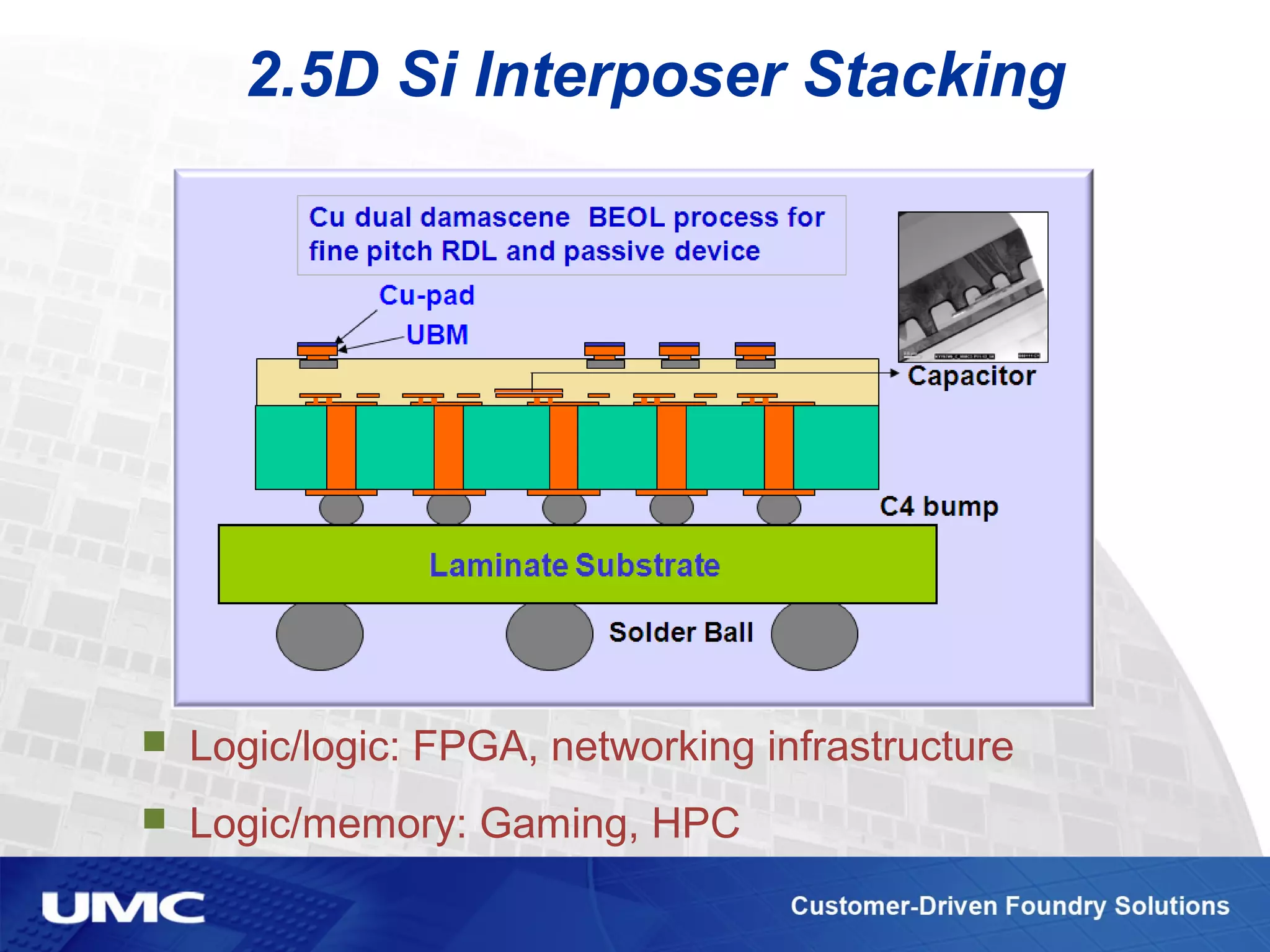
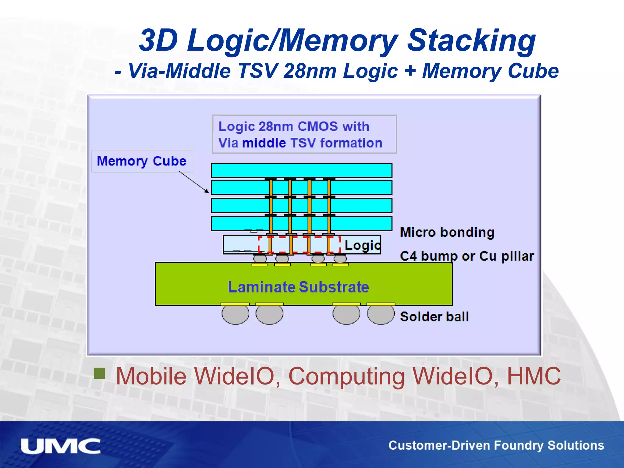
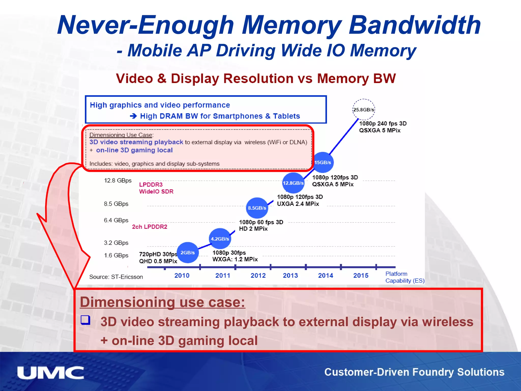
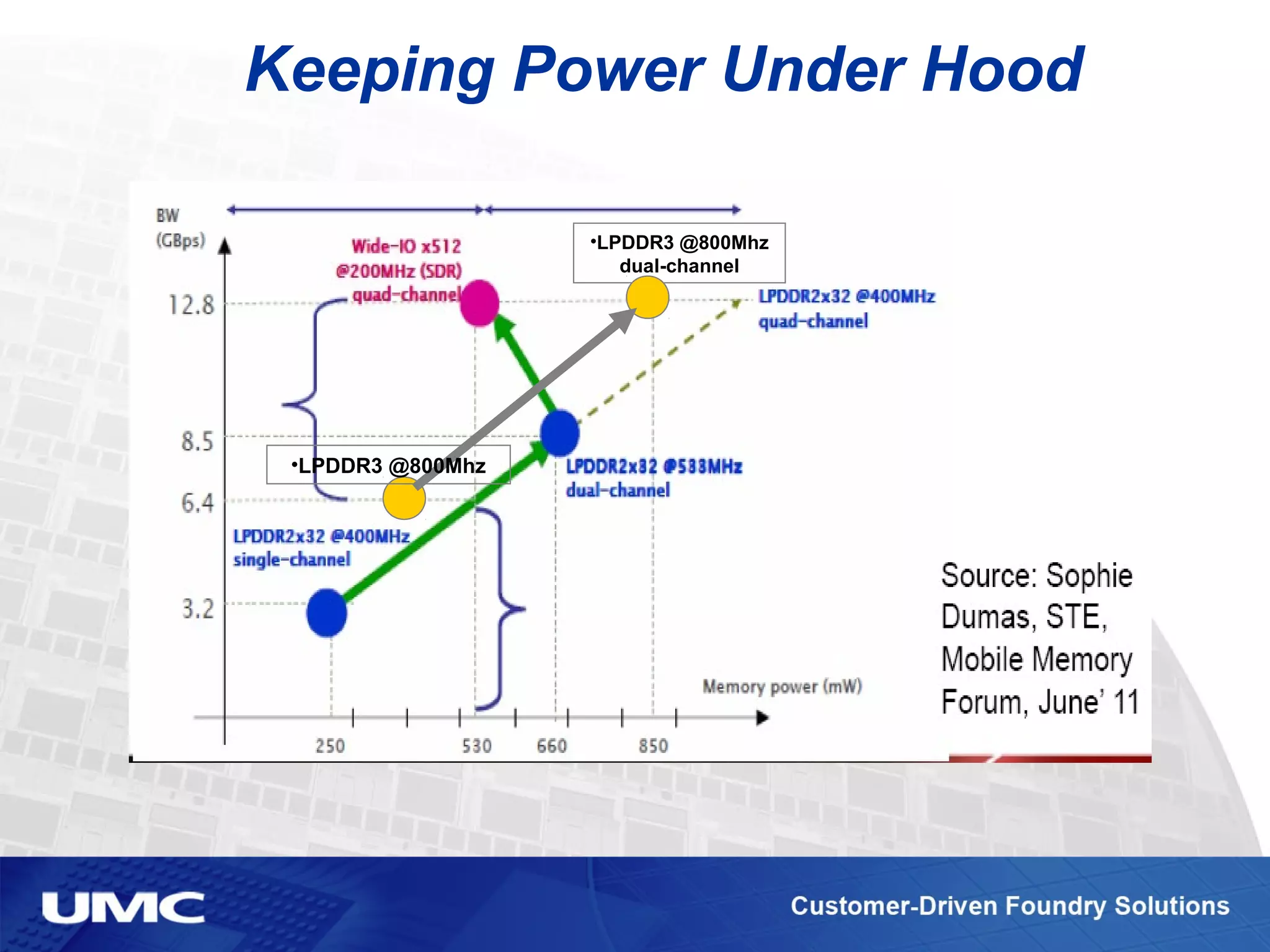
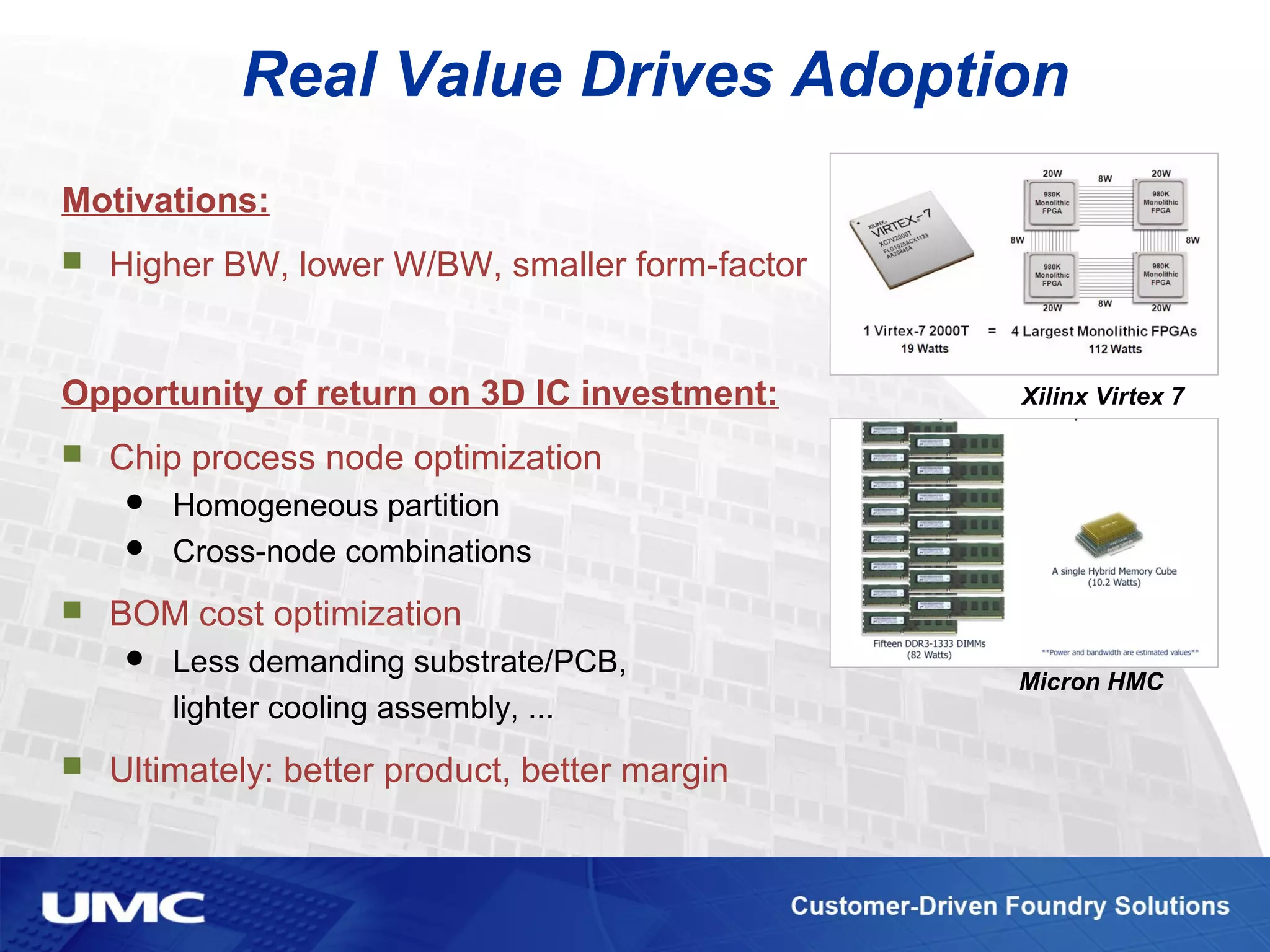
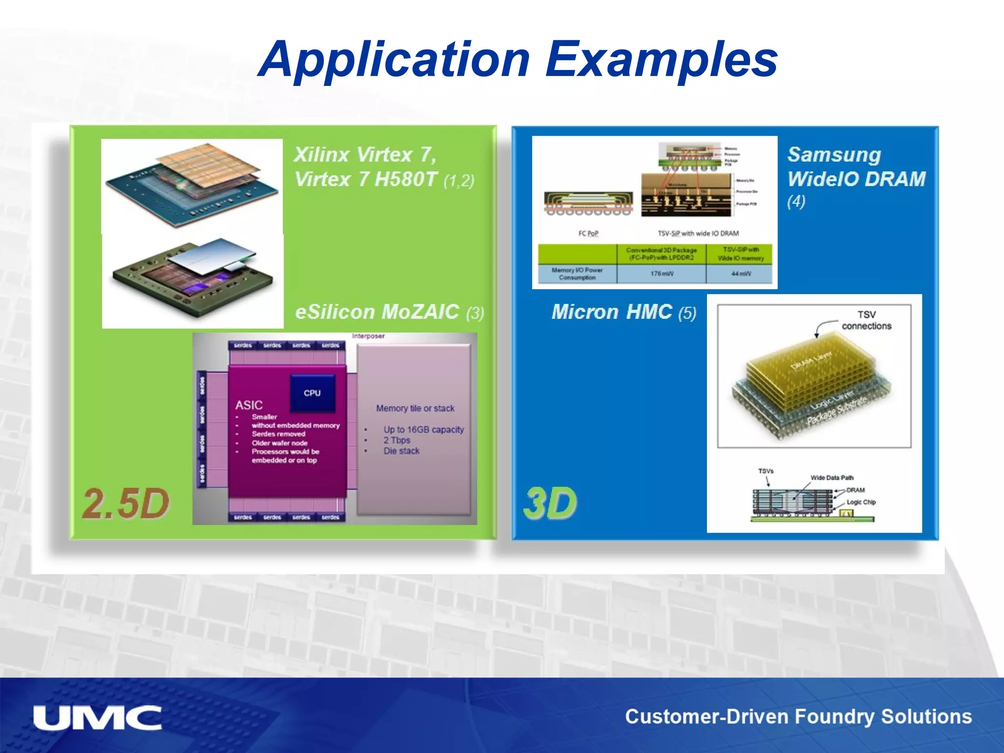
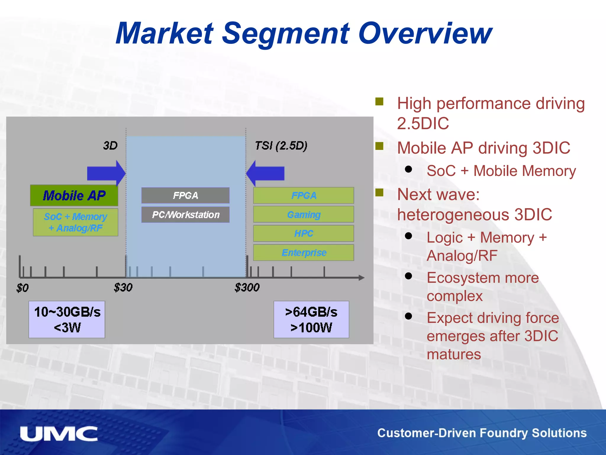
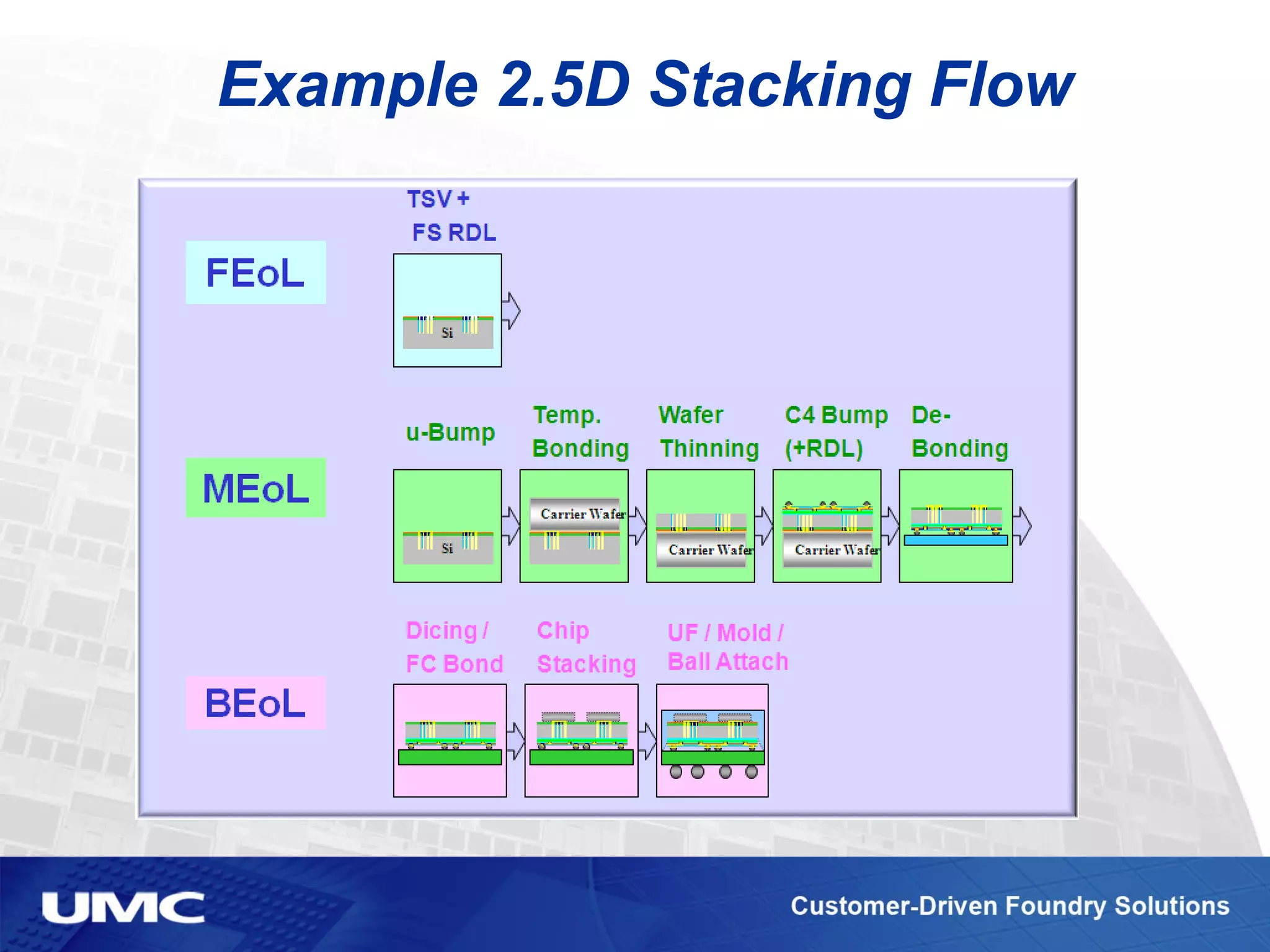
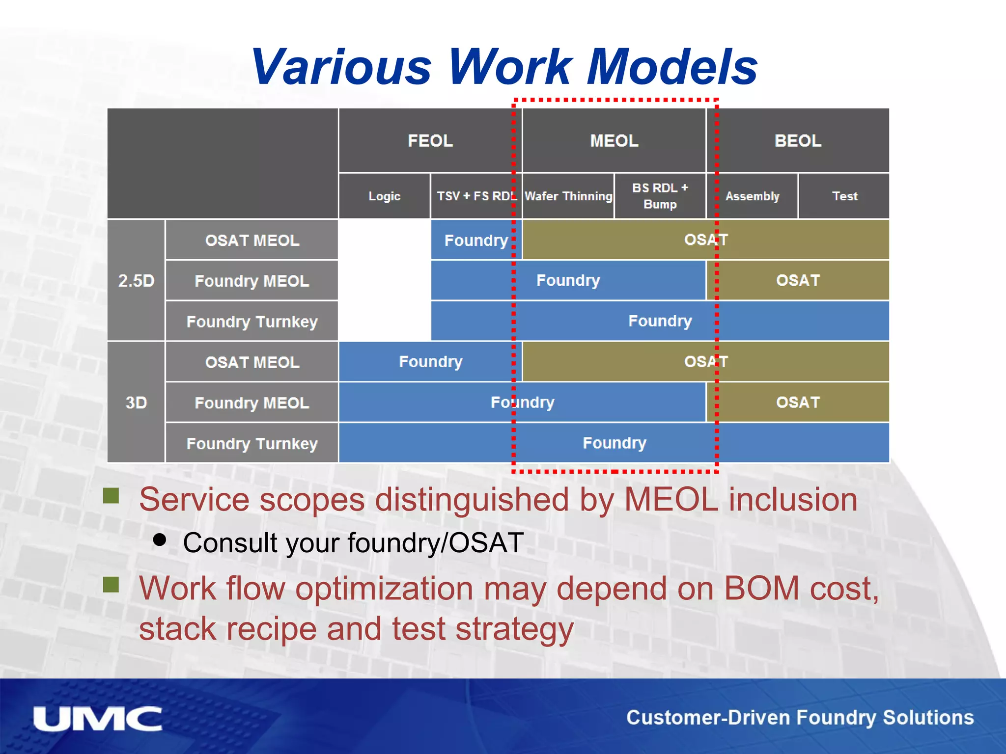
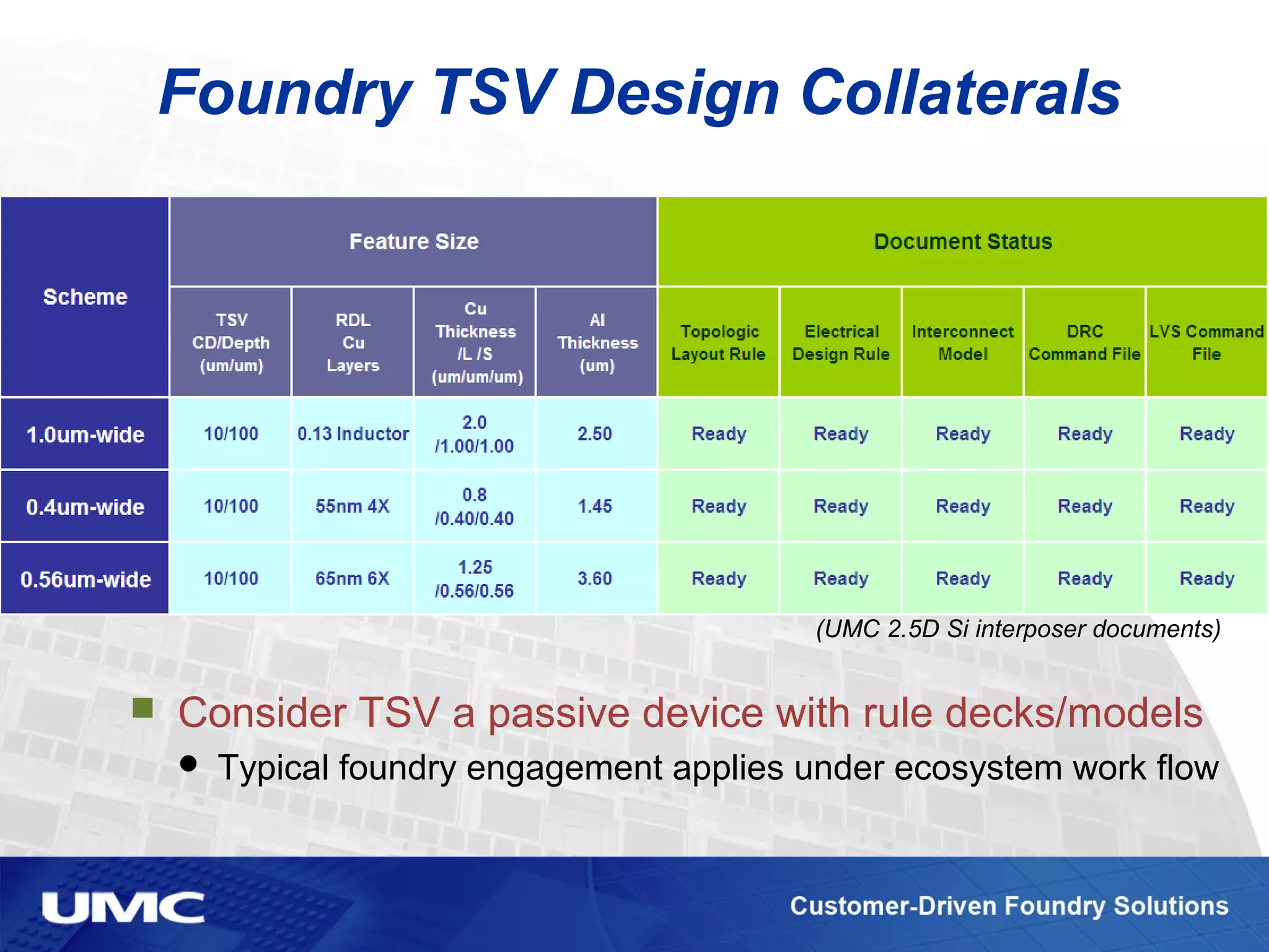
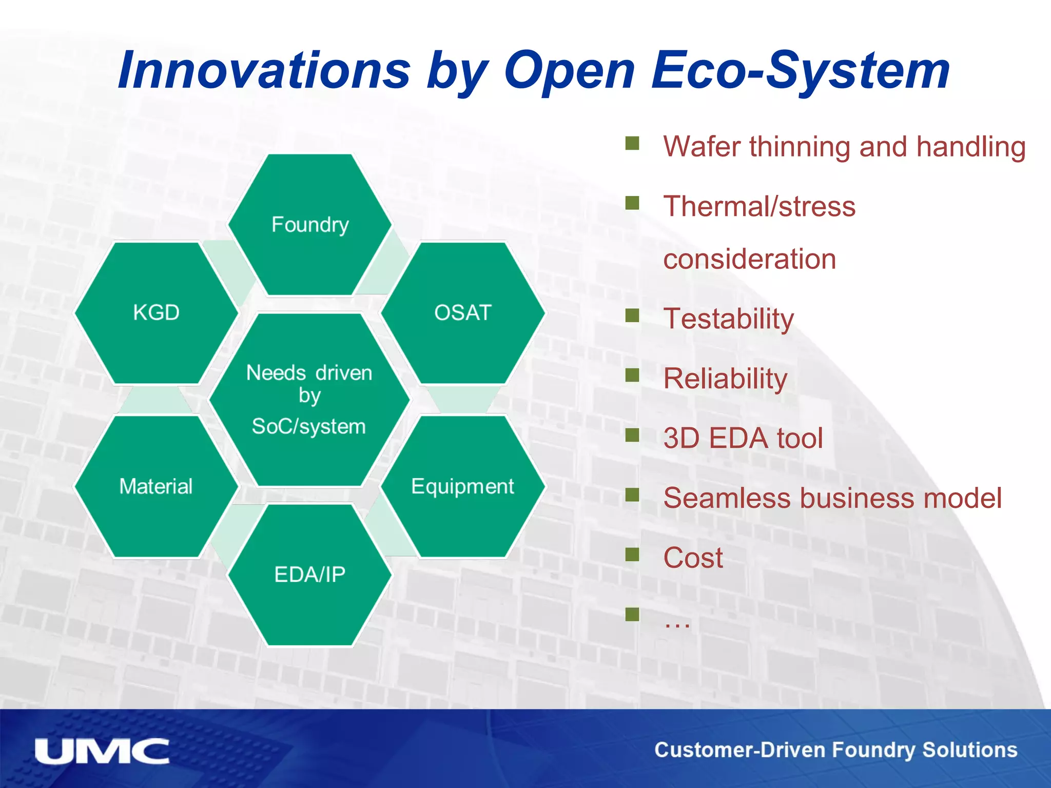
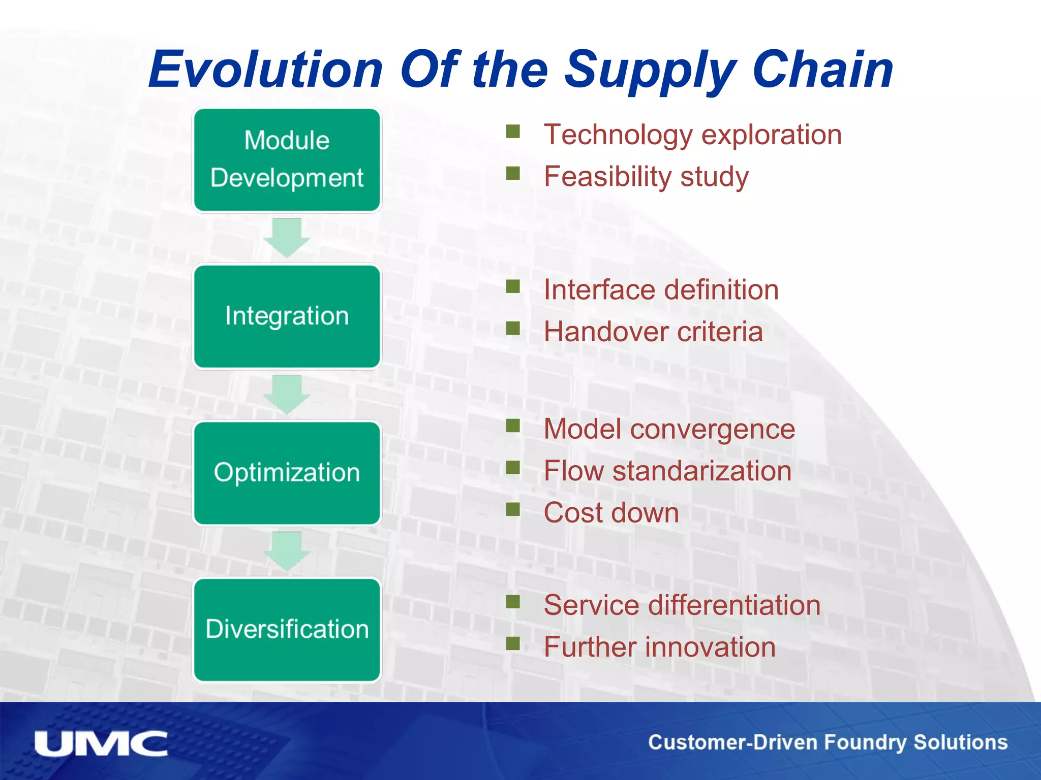
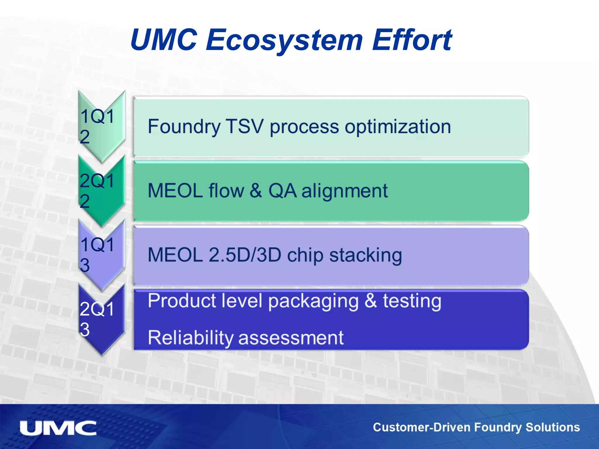
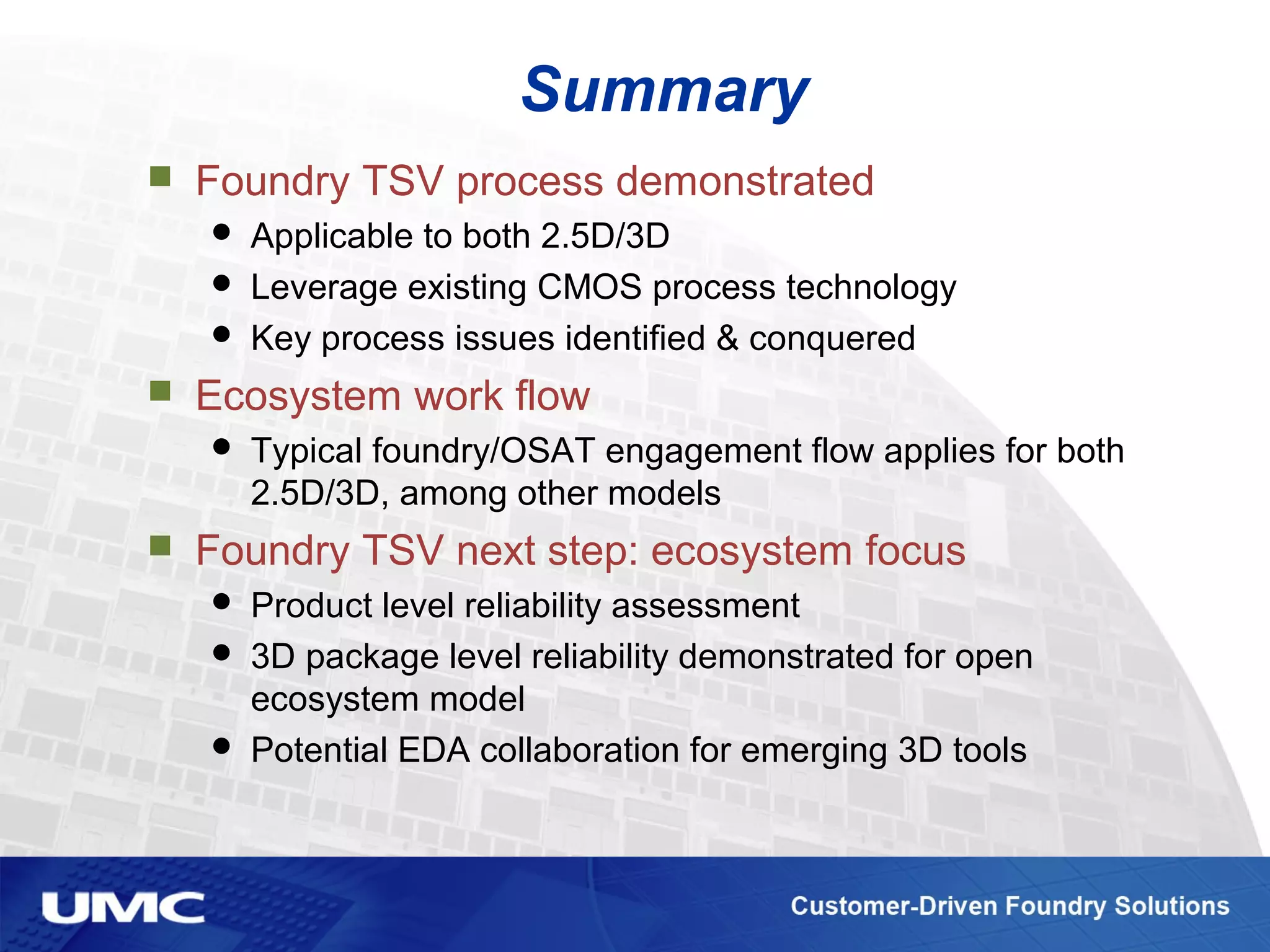
This document discusses 2.5D and 3D chip stacking technologies and the supply chain integration for their development. It outlines applications for 2.5D stacking of logic and memory chips as well as 3D stacking using through-silicon vias. The ecosystem workflow for 2.5D stacking is described, involving various partners from foundries to outsourced assembly and test houses. Finally, the document emphasizes that foundry development of through-silicon via processes has demonstrated key process issues can be identified and resolved, while ecosystem focus going forward includes product reliability assessment and collaboration on tools for 3D design.


![Vibe Coding vs. Spec-Driven Development [Free Meetup]](https://cdn.slidesharecdn.com/ss_thumbnails/vibecodingvsspecdrivendevelopment-251209105622-43f455e7-thumbnail.jpg?width=640&height=640&fit=bounds)


![Coded Agents – with UiPath SDK + LangGraph [Virtual Hands-on Workshop]](https://cdn.slidesharecdn.com/ss_thumbnails/codedagentsdeck-251215155422-5497c599-thumbnail.jpg?width=640&height=640&fit=bounds)